Photovoltaic cell and module physics and technology
|
|
|
- Georgina Wilcox
- 6 years ago
- Views:
Transcription
1 Photovoltaic cell and module physics and technology Vitezslav Benda, Prof Czech Technical University in Prague 6/21/2012 1
2 Outlines Photovoltaic Effect Photovoltaic cell structure and characteristics Photovoltaic cell construction and technology PV modules construction and technology Summary 6/21/2012 2


3 Solar energy TW Photovoltaics Direct transformation energy of solar irradiation into electricity
4 1. Light absorption in materials and excess carrier generation Photon energy h = hc/ (h is the Planck constant) photon momentum 0 Light is absorbed in the material. x (x) is the light intensity ( x) 0 exp( x) 0 exp xl = () is the absorption coefficient x L 1 x L is the so-called absorption length ( x) dx 0.68 ( x) dx Absorption is due to interactions with material particles (electrons and nucleus). If particle energy before interaction was W 1, after photon absorption is W 1 + h 0 0 interactions with the lattice results in an increase of temperature interactions with free electrons - results also in temperature increase interactions with bonded electrons- the incident light may generate some excess carriers (electron/hole pairs) 4

5 At interaction with photons of energy h W g are generated and carrier generation increases electron-hole pairs dn G( ; x) ( ) ( ) 0( )exp ( ) x dt gen n = n 0 + Δn, p = p 0 + Δp Excess carriers recombine with the recombination rate is so called carrier lifetime In dynamic equilibrium n = p = G dn R dt rec n
6 Efficiency of excess carrier generation by solar energy depens on the semiconductor band gap Suitable materials Silicon GaAs CuInSe 2 amorphous SiGe CdTe/CdS To obtain a potential difference that may be used as a source of electrical energy, an inhomogeneous structure with internal electric field is necessary. 6
7 Suitable structures with built-in electric field: p-type Junction Radiation n-type PN junction W c W g W F W v L n SCL L p heterojunction (contact of different materials). PIN structures
8 Principles of solar cell function In the illuminated area generated excess carriers diffuse towards the PN junction. The density J PV is created by carriers collected by the built-in electric field region J PV Total generated current density H H n ( ) qg( ; x) dx q dx J sr (0) J sr ( H ) 0 0 J sr is surface recombination JPV JPV ( ) d
9 Illuminated PN junction: supperposition of photo-generated current and PN junction (dark) I-V characteristic A I I in dark V OC irradiation V V I PV illuminated I SC Solar cell I-V chacteristic and its importan points V mp V OC PhotoVoltaic Power System Course May 2010, Aalborg University 9
10 Important solar cell electrical parameters open circuit voltage V OC, short circuit current I SC maximum output power V mp I mp fill factor V FF V mp OC I I mp SC V mp V OC efficiency Vmp I P in mp V OC I P SC in FF All parameters V OC, I SC, V mp, I mp, FF and η are usually given for standard testing conditions (STC): spectrum AM 1.5 radiation power 1000 W/m 2 cell temperature 25 C. PhotoVoltaic Power System Course May 2010, Aalborg University 10
11 Modelling I-V characteristics of a solar cell R s I Parallel resistance R p I PV D R p V R L Series resistance R S PN junction I-V characteristics J 01 n 2 i D q L n n 1 p p0 J qvj J 01 exp 1 1kT Dp 1 qnd i J L n 02 p n0 sc J 02 qvj exp 2kT Output cell voltage V = V j - R s I A - total cell area A ill illuminated cell area I V R I s s AillJ PV AJ q AJ q kt kt 01 exp 1 02 exp V R I V RsI R p
12 I (A) Influence of temperature For a high R p I 01 ~ n 2 i Consequently BT 3 V OC kt q W exp kt V OC T 0 For silicon cells the decrease of V OC is about 0.4%/K g ln I I PV V (V) 25 C 35 C 45 C 55 C 65 C 75 C 85 C 95 C R s increases with increasing temperature R p decreases with increasing temperature Both fill factor and efficiency decrease with temperature FF 0 0 T T At silicon cells 0.5% K T 1 1
13 The series resistance R s influences the cell efficiency At a constant irradiance


14 PV cell (module) with a low R s the efficiency increases with irradiance PV cell (module) with a high R s The efficiency decreases with increasing irradiance
15 To maximise current density J PV it is necessary maximise generation rate G minimise losses losses optical recombination electrical reflection shadowing not absorbed radiation emitter region base region surface series resistance parallel resistance 15
 -undirect (Si")

16 Two types of band structure -direct (GaAs like) -undirect (Si like) Basic types of solar cells: Crystalline silicon cells Thin film cells

 PV")


17 PV cells and modules from crystalline silicon (c-si) PV cells are realised from crystalline silicon wafers of thickness 0,15 0,25 mm and sides of mm c-si mono (37 %) Kerfs losses about 40% c-si multi (45 %)


18 Standard mass production (c-si cells) starting P-type wafers chemical surface texturing phosphorous diffusion SiN(H) antireflection surface coating and passivation contact grid realised by the screen print technique contact firing edge grinding cell measuring and sorting mono-crystalline 17% multi-crystalline 16%


19 Increasing cell efficiency Selective emitter Back contact cells Hetero junction cells (HIT)

20 A single solar cell ~0.5 V, about 30 ma/cm 2 For practical use it is necessary connect cells in series to obtain a source of higher voltage and in parallel to obtain a higher current Solar cell PV module PV field PhotoVoltaic Power System Course May 2010, Aalborg University 20
21 I (A) Cell connection in parallel R s R s R s R s R p R p R p R p Optimum situation: all cells have the same V MP If characteristics of individual cells in parallel differ, efficiency decreases ,0 0,1 0,2 0,3 0,4 0,5 0,6 0,7 V (V) 21
22 Cells in series.. the same current flows through all cells voltage does sums R s R s R s R s R p R p R p R p Simplified module model Optimum situation: all cells have the same I MP If characteristics of individual cells in series differ, efficiency decreases I I PV I V R I V R I ' ' s s 01exp q 1 I02 exp q 1 m 1 kt m 2kT V ' RsI R sh 22


23 PV c-si module technology soldering back covering foil (tedlar) EVA hardened glass 19
24 Module parameters open circuit voltage V OC, short circuit current I SC maximum output power V mp I mp fill factor V FF V mp OC I I mp SC Vmp I efficiency P in mp V OC STC (25 C, 1kW/m 2, AM 1,5) I P SC in FF NOCT (Nominal Operating Conditions Temperature) Ambient temperature 20 C, 800 W/m 2, wind 1 m/s

25 Basic types of solar cells: Crystalline silicon cells Thin film cells c on ta c t a ntire fle c tio n c o a tin g N -ty p e P -ty p e Suitable materials Basic problem: cost... CuInSe 2 amorphous silicon amorphous SiGe CdTe/CdS 25


26 Thin film solar cells CIS CdTe/CdS Amorphous Si Market share: 1.5% 5.7% 4.7% 26

27 Amorphous silicon solar cells TCO: SnO 2 ITO (indium-tin oxide) ZnO 600nm 1% <12% substrate TCO Light trapping TCO Ag or Al contact 27
28 Plasma enhanced CVD (PECVD) RF electrode and substrate create the capacitor structure. In this space the plasma and incorporated deposition of material on substrate takes place deposition of silicon nitride 3SiH 4 + 3NH 3 Si 3 N H 2 deposition polysilicon layers SiH 4 Si + 2H 2. 30
29 Thin film solar cell technology Amorphous (microcrystalline) silicon solar cells transparent substrate (glass) TCO a-si:h p+ layer (20-30 nm) a-si:h intrinsic ( 250 nm) a-si:h n+ layer (20 nm) TCO (diffusion barrier) Ag or Al SiH 4, H 2, B 2 H 6, PH 3, GeH 4, etc 31

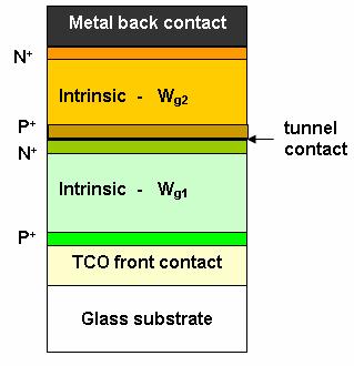
30 Tandem cells W g1 > W g2 irradiation 30


31 Thin film modules on glass substrates The module area is limited by the reaction chamber volume Very expensive equipment 35


32 Market share development 2011
33 PV module cost development Reduction of silicon cost USD/kg USD/kg USD/kg Reduction of C-Si module cost Thin-film modules are not cheaper than modules from crystalline silicon 33
Photovoltaic cell and module physics and technology. Vitezslav Benda, Prof Czech Technical University in Prague
 Photovoltaic cell and module physics and technology Vitezslav Benda, Prof Czech Technical University in Prague benda@fel.cvut.cz www.fel.cvut.cz 1 Outlines Photovoltaic Effect Photovoltaic cell structure
PHOTOVOLTAICS Fundamentals
 PHOTOVOLTAICS Fundamentals PV FUNDAMENTALS Semiconductor basics pn junction Solar cell operation Design of silicon solar cell SEMICONDUCTOR BASICS Allowed energy bands Valence and conduction band Fermi
EE 5611 Introduction to Microelectronic Technologies Fall Tuesday, September 23, 2014 Lecture 07
 EE 5611 Introduction to Microelectronic Technologies Fall 2014 Tuesday, September 23, 2014 Lecture 07 1 Introduction to Solar Cells Topics to be covered: Solar cells and sun light Review on semiconductor
Electrons are shared in covalent bonds between atoms of Si. A bound electron has the lowest energy state.
 Photovoltaics Basic Steps the generation of light-generated carriers; the collection of the light-generated carriers to generate a current; the generation of a large voltage across the solar cell; and
Chapter 7. Solar Cell
 Chapter 7 Solar Cell 7.0 Introduction Solar cells are useful for both space and terrestrial application. Solar cells furnish the long duration power supply for satellites. It converts sunlight directly
February 1, 2011 The University of Toledo, Department of Physics and Astronomy SSARE, PVIC
 FUNDAMENTAL PROPERTIES OF SOLAR CELLS February 1, 2011 The University of Toledo, Department of Physics and Astronomy SSARE, PVIC Principles and Varieties of Solar Energy (PHYS 4400) and Fundamentals of
FYS 3028/8028 Solar Energy and Energy Storage. Calculator with empty memory Language dictionaries
 Faculty of Science and Technology Exam in: FYS 3028/8028 Solar Energy and Energy Storage Date: 11.05.2016 Time: 9-13 Place: Åsgårdvegen 9 Approved aids: Type of sheets (sqares/lines): Number of pages incl.
Solar cells operation
 Solar cells operation photovoltaic effect light and dark V characteristics effect of intensity effect of temperature efficiency efficency losses reflection recombination carrier collection and quantum
Photovoltaic Energy Conversion. Frank Zimmermann
 Photovoltaic Energy Conversion Frank Zimmermann Solar Electricity Generation Consumes no fuel No pollution No greenhouse gases No moving parts, little or no maintenance Sunlight is plentiful & inexhaustible
MODELING THE FUNDAMENTAL LIMIT ON CONVERSION EFFICIENCY OF QD SOLAR CELLS
 MODELING THE FUNDAMENTAL LIMIT ON CONVERSION EFFICIENCY OF QD SOLAR CELLS Ա.Մ.Կեչիյանց Ara Kechiantz Institute of Radiophysics and Electronics (IRPhE), National Academy of Sciences (Yerevan, Armenia) Marseille
ET3034TUx Utilization of band gap energy
 ET3034TUx - 3.3.1 - Utilization of band gap energy In the last two weeks we have discussed the working principle of a solar cell and the external parameters that define the performance of a solar cell.
Lab #5 Current/Voltage Curves, Efficiency Measurements and Quantum Efficiency
 Lab #5 Current/Voltage Curves, Efficiency Measurements and Quantum Efficiency R.J. Ellingson and M.J. Heben November 4, 2014 PHYS 4580, 6280, and 7280 Simple solar cell structure The Diode Equation Ideal
High efficiency silicon and perovskite-silicon solar cells for electricity generation
 High efficiency silicon and perovskite-silicon solar cells for electricity generation Ali Dabirian Email: dabirian@ipm.ir 1 From Solar Energy to Electricity 2 Global accumulative PV installed In Iran it
OPTI510R: Photonics. Khanh Kieu College of Optical Sciences, University of Arizona Meinel building R.626
 OPTI510R: Photonics Khanh Kieu College of Optical Sciences, University of Arizona kkieu@optics.arizona.edu Meinel building R.626 Announcements Homework #6 is assigned, due May 1 st Final exam May 8, 10:30-12:30pm
Vikram L. Dalal Iowa State University Dept. of Elec. And Comp. Engr Iowa State University. All rights reserved.
 Growth Chemistry and Its Relationship to Amorphous Si Devices for Photovoltaic Energy Conversion Vikram L. Dalal Iowa State University Dept. of Elec. And Comp. Engr. 2002 Iowa State University. All rights
Thermionic Current Modeling and Equivalent Circuit of a III-V MQW P-I-N Photovoltaic Heterostructure
 Thermionic Current Modeling and Equivalent Circuit of a III-V MQW P-I-N Photovoltaic Heterostructure ARGYRIOS C. VARONIDES Physics and Electrical Engineering Department University of Scranton 800 Linden
Lecture 5 Junction characterisation
 Lecture 5 Junction characterisation Jon Major October 2018 The PV research cycle Make cells Measure cells Despair Repeat 40 1.1% 4.9% Data Current density (ma/cm 2 ) 20 0-20 -1.0-0.5 0.0 0.5 1.0 Voltage
Temperature Dependent Current-voltage Characteristics of P- type Crystalline Silicon Solar Cells Fabricated Using Screenprinting
 Temperature Dependent Current-voltage Characteristics of P- type Crystalline Silicon Solar Cells Fabricated Using Screenprinting Process Hyun-Jin Song, Won-Ki Lee, Chel-Jong Choi* School of Semiconductor
Paper Review. Special Topics in Optical Engineering II (15/1) Minkyu Kim. IEEE Journal of Quantum Electronics, Feb 1985
 Minkyu Kim. IEEE Journal of Quantum Electronics, Feb 1985") Paper Review IEEE Journal of Quantum Electronics, Feb 1985 Contents Semiconductor laser review High speed semiconductor laser Parasitic elements limitations Intermodulation products Intensity noise Large
Paper Review IEEE Journal of Quantum Electronics, Feb 1985 Contents Semiconductor laser review High speed semiconductor laser Parasitic elements limitations Intermodulation products Intensity noise Large
Mesoporous titanium dioxide electrolyte bulk heterojunction
 Mesoporous titanium dioxide electrolyte bulk heterojunction The term "bulk heterojunction" is used to describe a heterojunction composed of two different materials acting as electron- and a hole- transporters,
3.1 Absorption and Transparency
 3.1 Absorption and Transparency 3.1.1 Optical Devices (definitions) 3.1.2 Photon and Semiconductor Interactions 3.1.3 Photon Intensity 3.1.4 Absorption 3.1 Absorption and Transparency Objective 1: Recall
Fundamentals of Photovoltaics: C1 Problems. R.Treharne, K. Durose, J. Major, T. Veal, V.
 Fundamentals of Photovoltaics: C1 Problems R.Treharne, K. Durose, J. Major, T. Veal, V. Dhanak @cdtpv November 3, 2015 These problems will be highly relevant to the exam that you will sit very shortly.
A. K. Das Department of Physics, P. K. College, Contai; Contai , India.
 IOSR Journal of Applied Physics (IOSR-JAP) e-issn: 2278-4861.Volume 7, Issue 2 Ver. II (Mar. - Apr. 2015), PP 08-15 www.iosrjournals.org Efficiency Improvement of p-i-n Structure over p-n Structure and
Research Article Modeling and Optimization of Advanced Single- and Multijunction Solar Cells Based on Thin-Film a-si:h/sige Heterostructure
 International Scholarly Research Network ISRN Renewable Energy Volume 211, Article ID 712872, 8 pages doi:1.542/211/712872 Research Article Modeling and Optimization of Advanced Single- and Multijunction
Atmospheric pressure Plasma Enhanced CVD for large area deposition of TiO 2-x electron transport layers for PV. Heather M. Yates
 Atmospheric pressure Plasma Enhanced CVD for large area deposition of TiO 2-x electron transport layers for PV Heather M. Yates Why the interest? Perovskite solar cells have shown considerable promise
LEC E T C U T R U E R E 17 -Photodetectors
 LECTURE 17 -Photodetectors Topics to be covered Photodetectors PIN photodiode Avalanche Photodiode Photodetectors Principle of the p-n junction Photodiode A generic photodiode. Photodetectors Principle
Investigation of Thin Film Solar Cells on CdS/CdTe Base with Different Back Contacts
 CIMTEC Forum 2010 (0) 5 pages (0) Trans Tech Publications, Switzerland Investigation of Thin Film Solar Cells on CdS/CdTe Base with Different Back Contacts G. Khrypunov 1, A. Meriuts 1, H. Klochko 1, T.
Comparison of Ge, InGaAs p-n junction solar cell
 ournal of Physics: Conference Series PAPER OPEN ACCESS Comparison of Ge, InGaAs p-n junction solar cell To cite this article: M. Korun and T. S. Navruz 16. Phys.: Conf. Ser. 77 135 View the article online
Chemistry Instrumental Analysis Lecture 8. Chem 4631
 Chemistry 4631 Instrumental Analysis Lecture 8 UV to IR Components of Optical Basic components of spectroscopic instruments: stable source of radiant energy transparent container to hold sample device
EE495/695 Introduction to Semiconductors I. Y. Baghzouz ECE Department UNLV
 EE495/695 Introduction to Semiconductors I Y. Baghzouz ECE Department UNLV Introduction Solar cells have always been aligned closely with other electronic devices. We will cover the basic aspects of semiconductor
Introduction. Katarzyna Skorupska. Silicon will be used as the model material however presented knowledge applies to other semiconducting materials
 Introduction Katarzyna Skorupska Silicon will be used as the model material however presented knowledge applies to other semiconducting materials 2 June 26 Intrinsic and Doped Semiconductors 3 July 3 Optical
AMPS - 1D. A. K. Das Department of Physics, P. K. College, Contai; Contai , India.
 IOSR Journal of Applied Physics (IOSRJAP) eissn: 22784861.Volume 7, Issue 1 Ver. II (Jan.Feb. 2015), PP 2330 www.iosrjournals.org Numerical Simulation of Si 1 x Ge x Thin Film Solar Cell Using AMPS 1D
Chapter 3 Modeling and Simulation of Dye-Sensitized Solar Cell
 Chapter 3 Modeling and Simulation of Dye-Sensitized Solar Cell 3.1. Introduction In recent years, dye-sensitized solar cells (DSSCs) based on nanocrystalline mesoporous TiO 2 films have attracted much
Semiconductor Junctions
 8 Semiconductor Junctions Almost all solar cells contain junctions between different materials of different doping. Since these junctions are crucial to the operation of the solar cell, we will discuss
EE 5344 Introduction to MEMS CHAPTER 5 Radiation Sensors
 EE 5344 Introduction to MEMS CHAPTER 5 Radiation Sensors 5. Radiation Microsensors Radiation µ-sensors convert incident radiant signals into standard electrical out put signals. Radiant Signals Classification
Quiz #1 Practice Problem Set
 Name: Student Number: ELEC 3908 Physical Electronics Quiz #1 Practice Problem Set? Minutes January 22, 2016 - No aids except a non-programmable calculator - All questions must be answered - All questions
(Co-PIs-Mark Brongersma, Yi Cui, Shanhui Fan) Stanford University. GCEP Research Symposium 2013 Stanford, CA October 9, 2013
 Stanford University. GCEP Research Symposium 2013 Stanford, CA October 9, 2013") High-efficiency thin film nano-structured multi-junction solar James S. cells Harris (PI) (Co-PIs-Mark Brongersma, Yi Cui, Shanhui Fan) Stanford University GCEP Research Symposium 2013 Stanford, CA October
High-efficiency thin film nano-structured multi-junction solar James S. cells Harris (PI) (Co-PIs-Mark Brongersma, Yi Cui, Shanhui Fan) Stanford University GCEP Research Symposium 2013 Stanford, CA October
3.1 Introduction to Semiconductors. Y. Baghzouz ECE Department UNLV
 3.1 Introduction to Semiconductors Y. Baghzouz ECE Department UNLV Introduction In this lecture, we will cover the basic aspects of semiconductor materials, and the physical mechanisms which are at the
Plasma Deposition (Overview) Lecture 1
 Lecture 1") Plasma Deposition (Overview) Lecture 1 Material Processes Plasma Processing Plasma-assisted Deposition Implantation Surface Modification Development of Plasma-based processing Microelectronics needs (fabrication
Plasma Deposition (Overview) Lecture 1 Material Processes Plasma Processing Plasma-assisted Deposition Implantation Surface Modification Development of Plasma-based processing Microelectronics needs (fabrication
EE 6313 Homework Assignments
 EE 6313 Homework Assignments 1. Homework I: Chapter 1: 1.2, 1.5, 1.7, 1.10, 1.12 [Lattice constant only] (Due Sept. 1, 2009). 2. Homework II: Chapter 1, 2: 1.17, 2.1 (a, c) (k = π/a at zone edge), 2.3
Lecture 15: Optoelectronic devices: Introduction
 Lecture 15: Optoelectronic devices: Introduction Contents 1 Optical absorption 1 1.1 Absorption coefficient....................... 2 2 Optical recombination 5 3 Recombination and carrier lifetime 6 3.1
3.003 Principles of Engineering Practice
 3.003 Principles of Engineering Practice One Month Review Solar Cells The Sun Semiconductors pn junctions Electricity 1 Engineering Practice 1. Problem Definition 2. Constraints 3. Options 4. Analysis
Silicon Concentrator Solar Cells: Fabrication, Characterization and Development of Innovative Designs.
 University of Trento Department of Physics Doctoral School in Physics, XXV cycle Phd Thesis Silicon Concentrator Solar Cells: Fabrication, Characterization and Development of Innovative Designs. Candidate:
Technology Options for Photo voltaic Solar Cells. Claudio Fiegna
 Technology Options for Photo voltaic Solar Cells Claudio Fiegna Outline Introduction Working principle for solar cells Silicon based solar cells Crystalline Thin film a Si or c Si Other thin film technologies
1 Name: Student number: DEPARTMENT OF PHYSICS AND PHYSICAL OCEANOGRAPHY MEMORIAL UNIVERSITY OF NEWFOUNDLAND. Fall :00-11:00
 1 Name: DEPARTMENT OF PHYSICS AND PHYSICAL OCEANOGRAPHY MEMORIAL UNIVERSITY OF NEWFOUNDLAND Final Exam Physics 3000 December 11, 2012 Fall 2012 9:00-11:00 INSTRUCTIONS: 1. Answer all seven (7) questions.
Fundamental Limitations of Solar Cells
 2018 Lecture 2 Fundamental Limitations of Solar Cells Dr Kieran Cheetham MPhys (hons) CPhys MInstP MIET L3 Key Question Why can't a solar cell have a 100% efficiency? (Or even close to 100%?) Can you answer
Solar Photovoltaics & Energy Systems
 Solar Photovoltaics & Energy Systems Lecture 3. Crystalline Semiconductor Based Solar Cells ChE-600 Wolfgang Tress, March 2018 1 Photovoltaic Solar Energy Conversion 2 Outline Recap: Thermodynamics of
Third generation solar cells - How to use all the pretty colours?
 Third generation solar cells - How to use all the pretty colours? Erik Stensrud Marstein Department for Solar Energy Overview The trouble with conventional solar cells Third generation solar cell concepts
Charge Extraction. Lecture 9 10/06/2011 MIT Fundamentals of Photovoltaics 2.626/2.627 Fall 2011 Prof. Tonio Buonassisi
 Charge Extraction Lecture 9 10/06/2011 MIT Fundamentals of Photovoltaics 2.626/2.627 Fall 2011 Prof. Tonio Buonassisi 2.626/2.627 Roadmap You Are Here 2.626/2.627: Fundamentals Every photovoltaic device
Solar Photovoltaics & Energy Systems
 Solar Photovoltaics & Energy Systems Lecture 4. Crystalline Semiconductor Based Solar Cells ChE-600 Wolfgang Tress, May 2016 1 Photovoltaic Solar Energy Conversion 2 Semiconductor vs. Heat Engine spectral
26% PK/silicon tandem solar cell with 1 cm 2 area H2020-LCE
 H2020-LCE-205- CHEOPS Production Technology to Achieve Low Cost and Highly Efficient Photovoltaic Perovskite Solar Cells Deliverable WP4 PK/c-Si SHJ tandem device development Author: Arnaud Walter (CSEM)
Photovoltaic Devices. Content
 Photovoltaic Devices EPFL IMT - PVLab Highlights in Microtechnology, 2014 Content Applications overviews Brief history Basics of photovoltaics (PV) Physical principle and performance limits Multi-junction
Solar Cells Technology: An Engine for National Development
 IOSR Journal of Electrical and Electronics Engineering (IOSR-JEEE) e-issn: 2278-1676,p-ISSN: 2320-3331, Volume 7, Issue 5 (Sep. - Oct. 2013), PP 13-18 Solar Cells Technology: An Engine for National Development
The photovoltaic effect occurs in semiconductors where there are distinct valence and
 How a Photovoltaic Cell Works The photovoltaic effect occurs in semiconductors where there are distinct valence and conduction bands. (There are energies at which electrons can not exist within the solid)
Novel Inorganic-Organic Perovskites for Solution Processed Photovoltaics. PIs: Mike McGehee and Hema Karunadasa
 Novel Inorganic-Organic Perovskites for Solution Processed Photovoltaics PIs: Mike McGehee and Hema Karunadasa 1 Perovskite Solar Cells are Soaring Jul 2013 Grätzel, EPFL 15% Nov 2014 KRICT 20.1%! Seok,
Spectroscopic Ellipsometry (SE) in Photovoltaic Applications
 in Photovoltaic Applications") Spectroscopic Ellipsometry (SE) in Photovoltaic Applications Jianing Sun, James Hilfiker, Greg Pribil, and John Woollam c-si PVMC Metrology Workshop July 2012, San Francisco PV key issues Material selection
Spectroscopic Ellipsometry (SE) in Photovoltaic Applications Jianing Sun, James Hilfiker, Greg Pribil, and John Woollam c-si PVMC Metrology Workshop July 2012, San Francisco PV key issues Material selection
Novel High-Efficiency Crystalline-Si-Based Compound. Heterojunction Solar Cells: HCT (Heterojunction with Compound. Thin-layer)
") Electronic Supplementary Material (ESI) for Physical Chemistry Chemical Physics. This journal is the Owner Societies 2014 Supplementary Information for Novel High-Efficiency Crystalline-Si-Based Compound
Electronic Supplementary Material (ESI) for Physical Chemistry Chemical Physics. This journal is the Owner Societies 2014 Supplementary Information for Novel High-Efficiency Crystalline-Si-Based Compound
Graded S i N x /S i O x N y Layers as Antireflective Coatings for Solar Cells Based on GaAs and Silicon Crystalline
 Science Research 2016; 4(1): 21-25 Published online February 25, 2016 (http://www.sciencepublishinggroup.com/j/sr) doi: 10.11648/j.sr.20160401.14 ISSN: 2329-0935 (Print); ISSN: 2329-0927 (Online) Graded
Supporting Information
 Electronic Supplementary Material (ESI) for Journal of Materials Chemistry A. This journal is The Royal Society of Chemistry 2018 Supporting Information A minimal non-radiative recombination loss for efficient
Electronic Supplementary Information. Recombination kinetics in silicon solar cell under low-concentration: Electroanalytical
 Electronic Supplementary Material (ESI) for Physical Chemistry Chemical Physics. This journal is the Owner Societies 2014 Electronic Supplementary Information Recombination kinetics in silicon solar cell
Self-study problems and questions Processing and Device Technology, FFF110/FYSD13
 Self-study problems and questions Processing and Device Technology, FFF110/FYSD13 Version 2016_01 In addition to the problems discussed at the seminars and at the lectures, you can use this set of problems
Organic Electronic Devices
 Organic Electronic Devices Week 4: Organic Photovoltaic Devices Lecture 4.2: Characterizing Device Parameters in OPVs Bryan W. Boudouris Chemical Engineering Purdue University 1 Lecture Overview and Learning
Goal for next generation solar cells: Efficiencies greater than Si with low cost (low temperature) processing
 processing") Multi-junction cells MBE growth > 40% efficient Expensive Single crystal Si >20% efficient expensive Thin film cells >10% efficient Less expensive Toxic materials Polymers
Multi-junction cells MBE growth > 40% efficient Expensive Single crystal Si >20% efficient expensive Thin film cells >10% efficient Less expensive Toxic materials Polymers
Lab 2. Characterization of Solar Cells
 Lab 2. Characterization of Solar Cells Physics Enhancement Programme Department of Physics, Hong Kong Baptist University 1. OBJECTIVES To familiarize with the principles of commercial solar cells To characterize
Two-dimensional lattice
 Two-dimensional lattice a 1 *, k x k x =0,k y =0 X M a 2, y Γ X a 2 *, k y a 1, x Reciprocal lattice Γ k x = 0.5 a 1 *, k y =0 k x = 0, k y = 0.5 a 2 * k x =0.5a 1 *, k y =0.5a 2 * X X M k x = 0.25 a 1
Maria Carmela Di Piazza. Gianpaolo Vitale. Photovoltaic Sources. Modeling and Emulation. ^ Springer
 Maria Carmela Di Piazza Gianpaolo Vitale Photovoltaic Sources Modeling and Emulation ^ Springer Part I 1 From the Nuclear Fusion to the Radiated Energy on the Earth... 3 1.1 Inside the Universe 3 1.2 The
The Opto-Electronic Physics That Just Broke the Efficiency Record in Solar Cells
 The Opto-Electronic Physics That Just Broke the Efficiency Record in Solar Cells Solar Energy Mini-Series Jen-Hsun Huang Engineering Center Stanford, California Sept. 26, 2011 Owen D. Miller & Eli Yablonovitch
The Current Status of Perovskite Solar Cell Research at UCLA
 The Current Status of Perovskite Solar Cell Research at UCLA Lijian Zuo, Sanghoon Bae, Lei Meng, Yaowen Li, and Yang Yang* Department of Materials Science and Engineering University of California, Los
Challenges in to-electric Energy Conversion: an Introduction
 Challenges in Solar-to to-electric Energy Conversion: an Introduction Eray S. Aydil Chemical Engineering and Materials Science Department Acknowledgements: National Science Foundation Minnesota Initiative
Opto-electronic Characterization of Perovskite Thin Films & Solar Cells
 Opto-electronic Characterization of Perovskite Thin Films & Solar Cells Arman Mahboubi Soufiani Supervisors: Prof. Martin Green Prof. Gavin Conibeer Dr. Anita Ho-Baillie Dr. Murad Tayebjee 22 nd June 2017
Photon absorption and creation of electron-hole pairs
 UCONN ENGR_ECE 4243-6243 Course outline Chapter 15 F. Jain L13 11292016-Solar Cells Part (Sections 6.1-6.8) L14 Solar cells Part- Tandem cells, MEG, and QD Solar Cells Notes page Slide# 6.1. ntroduction
The Shockley-Queisser Limit. Jake Friedlein 7 Dec. 2012
 The Shockley-Queisser Limit Jake Friedlein 7 Dec. 2012 1 Outline A. Loss factors 1. Bandgap energy 2. Geometric factor 3. Recombination of electrons and holes B. Overall efficiency C. Optimum bandgap 2
Photogating effect observed in microcrystalline silicon solar cells and its applications in cell optimization
 6 Photogating effect observed in microcrystalline silicon solar cells and its applications in cell optimization As we discussed in the previous Chapters, quantum efficiency measurement is of great importance
Organic solar cells with inverted layer sequence incorporating optical spacers - simulation and experiment.
 Organic solar cells with inverted layer sequence incorporating optical spacers - simulation and experiment. Birger Zimmermann a, Markus Glatthaar a, Michael Niggemann Author3 a,b, Moritz Kilian Riede b,
Lecture 2. Photon in, Electron out: Basic Principle of PV
 Lecture 2 Photon in, Electron out: Basic Principle of PV References: 1. Physics of Solar Cells. Jenny Nelson. Imperial College Press, 2003. 2. Third Generation Photovoltaics: Advanced Solar Energy Conversion.
Towards a deeper understanding of polymer solar cells
 Towards a deeper understanding of polymer solar cells Jan Anton Koster Valentin Mihailetchi Prof. Paul Blom Molecular Electronics Zernike Institute for Advanced Materials and DPI University of Groningen
e - Galvanic Cell 1. Voltage Sources 1.1 Polymer Electrolyte Membrane (PEM) Fuel Cell
 Fuel Cell") Galvanic cells convert different forms of energy (chemical fuel, sunlight, mechanical pressure, etc.) into electrical energy and heat. In this lecture, we are interested in some examples of galvanic cells.
Galvanic cells convert different forms of energy (chemical fuel, sunlight, mechanical pressure, etc.) into electrical energy and heat. In this lecture, we are interested in some examples of galvanic cells.
Lecture 12. Semiconductor Detectors - Photodetectors
 Lecture 12 Semiconductor Detectors - Photodetectors Principle of the pn junction photodiode Absorption coefficient and photodiode materials Properties of semiconductor detectors The pin photodiodes Avalanche
SEMICONDUCTOR HETEROJUNCTIONS
 SEMICONDUCTOR HETEROJUNCTIONS February 14, 2012 The University of Toledo, Department of Physics and Astronomy SSARE, PVIC Principles and Varieties of Solar Energy (PHYS 4400) and Fundamentals of Solar
Analyze the effect of window layer (AlAs) for increasing the efficiency of GaAs based solar cell
 for increasing the efficiency of GaAs based solar cell") American Journal of Engineering Research (AJER) e-issn: 2320-0847 p-issn : 2320-0936 Volume-4, Issue-7, pp-304-315 www.ajer.org Research Paper Open Access Analyze the effect of window layer (AlAs) for
American Journal of Engineering Research (AJER) e-issn: 2320-0847 p-issn : 2320-0936 Volume-4, Issue-7, pp-304-315 www.ajer.org Research Paper Open Access Analyze the effect of window layer (AlAs) for
EE130: Integrated Circuit Devices
 EE130: Integrated Circuit Devices (online at http://webcast.berkeley.edu) Instructor: Prof. Tsu-Jae King (tking@eecs.berkeley.edu) TA s: Marie Eyoum (meyoum@eecs.berkeley.edu) Alvaro Padilla (apadilla@eecs.berkeley.edu)
Designing Information Devices and Systems II A. Sahai, J. Roychowdhury, K. Pister Discussion 1A
 EECS 16B Spring 2019 Designing Information Devices and Systems II A. Sahai, J. Roychowdhury, K. Pister Discussion 1A 1 Semiconductor Physics Generally, semiconductors are crystalline solids bonded into
Toward a 1D Device Model Part 1: Device Fundamentals
 Toward a 1D Device Model Part 1: Device Fundamentals Lecture 7 9/29/2011 MIT Fundamentals of Photovoltaics 2.626/2.627 Fall 2011 Prof. Tonio Buonassisi 1 Learning Objectives: Toward a 1D Device Model 1.
Plastic Electronics. Joaquim Puigdollers.
 Plastic Electronics Joaquim Puigdollers Joaquim.puigdollers@upc.edu Nobel Prize Chemistry 2000 Origins Technological Interest First products.. MONOCROMATIC PHILIPS Today Future Technological interest Low
Energy level diagram for the p n junction in thermal equilibrium Electric field
 pn JUNCTION Energy level diagram for the p n junction in thermal equilibrium Electric field E C E F E V p type Electron Drift Neutral p region Hole Diffusion +++ +++ +++ +++ +++ +++ +++ +++ +++ +++ +++
Uwe Rau Institut für Energieforschung 5 Photovoltaik- Forschungszentrum Jülich GmbH
 Mitglied der Helmholtz-Gemeinschaft Materialforschung für f r DünnschichtphotovoltaikD nnschichtphotovoltaik- Status und neue Entwicklungen Uwe Rau Institut für Energieforschung 5 Photovoltaik- Forschungszentrum
Organic solar cells. State of the art and outlooks. Gilles Horowitz LPICM, UMR7647 CNRS - Ecole Polytechnique
 Organic solar cells. State of the art and outlooks Gilles Horowitz LPICM, UMR7647 CNRS - Ecole Polytechnique Solar energy Solar energy on earth: 75,000 tep/year 6000 times the world consumption in 2007
Chapter 1. Solar energy conversion: from amorphous silicon to Dye-Sensitized Solar Cells. 1.1 Photovoltaic history.
 Chapter 1 Solar energy conversion: from amorphous silicon to Dye-Sensitized Solar Cells 1.1 Photovoltaic history. 1.2 Operation of traditional photovoltaic devices. 1.3 Thin film solar cells. 1.4 Multijunction
Photosynthesis & Solar Power Harvesting
 Lecture 23 Semiconductor Detectors - Photodetectors Principle of the pn junction photodiode Absorption coefficient and photodiode materials Properties of semiconductor detectors The pin photodiodes Avalanche
The temperature dependence of the spectral and e ciency behavior of Si solar cell under low concentrated solar radiation
 Renewable Energy 21 (2000) 445±458 www.elsevier.com/locate/renene The temperature dependence of the spectral and e ciency behavior of Si solar cell under low concentrated solar radiation M.A. Mosalam Shaltout
Lecture 1. OUTLINE Basic Semiconductor Physics. Reading: Chapter 2.1. Semiconductors Intrinsic (undoped) silicon Doping Carrier concentrations
 silicon Doping Carrier concentrations") Lecture 1 OUTLINE Basic Semiconductor Physics Semiconductors Intrinsic (undoped) silicon Doping Carrier concentrations Reading: Chapter 2.1 EE105 Fall 2007 Lecture 1, Slide 1 What is a Semiconductor? Low
Lecture 1 OUTLINE Basic Semiconductor Physics Semiconductors Intrinsic (undoped) silicon Doping Carrier concentrations Reading: Chapter 2.1 EE105 Fall 2007 Lecture 1, Slide 1 What is a Semiconductor? Low
Lecture 2. Introduction to semiconductors Structures and characteristics in semiconductors
 Lecture 2 Introduction to semiconductors Structures and characteristics in semiconductors Semiconductor p-n junction Metal Oxide Silicon structure Semiconductor contact Literature Glen F. Knoll, Radiation
Quiz #1 Due 9:30am Session #10. Quiz Instructions
 2.626/2.627 Fall 2011 Fundamentals of Photovoltaics Quiz #1 Due 9:30am Session #10 Quiz Instructions The undergraduate version of this quiz (2.627) consists of four (4) multipart questions for a point
The Opto-Electronic Physics Which Just Broke the Efficiency Record in Solar Cells. Green Photonics Symposium at Technion Haifa, Israel, April 23, 2014
 The Opto-Electronic Physics Which Just Broke the Efficiency Record in Solar Cells Green Photonics Symposium at Technion Haifa, Israel, April 23, 2014 Eli Yablonovitch UC Berkeley Electrical Engineering
Planar Organic Photovoltaic Device. Saiful I. Khondaker
 Planar Organic Photovoltaic Device Saiful I. Khondaker Nanoscience Technology Center and Department of Physics University of Central Florida http://www.physics.ucf.edu/~khondaker W Metal 1 L ch Metal 2
Classification of Solids
 Classification of Solids Classification by conductivity, which is related to the band structure: (Filled bands are shown dark; D(E) = Density of states) Class Electron Density Density of States D(E) Examples
Charge Carriers in Semiconductor
 Charge Carriers in Semiconductor To understand PN junction s IV characteristics, it is important to understand charge carriers behavior in solids, how to modify carrier densities, and different mechanisms
A SOLID STATE PYRANOMETER. Anca Laura Dumitrescu, Marius Paulescu, Aurel Ercuta
 Analele Universităţii de Vest din Timişoara Vol. LVIII, 2015 Seria Fizică OI: 10.1515/awutp -2015-0207 A SOLI STATE PYRANOMETER Anca Laura umitrescu, Marius Paulescu, Aurel Ercuta Faculty of Physics, West
EE 446/646 Photovoltaic Devices I. Y. Baghzouz
 EE 446/646 Photovoltaic Devices I Y. Baghzouz What is Photovoltaics? First used in about 1890, the word has two parts: photo, derived from the Greek word for light, volt, relating to electricity pioneer
STUDY OF THE PERFORMANCES OF A TANDEM PHOTOVOLTAIC CELL BASED ON CIGS
 Journal of Ovonic Research Vol. 15, No. 1, January February 2019, p. 43-52 STUDY OF THE PERFORMANCES OF A TANDEM PHOTOVOLTAIC CELL BASED ON CIGS B. MERAH a,*, H. KHACHAB b, A. HEMMANI b, M. BOUSSERHANE