Magnetic core memory (1951) cm 2 ( bit)
|
|
|
- Evangeline Andrews
- 5 years ago
- Views:
Transcription


1 Magnetic core memory (1951) cm 2 ( bit)
2
3 Semiconductor Memory Classification Read-Write Memory Non-Volatile Read-Write Memory Read-Only Memory Random Access Non-Random Access EPROM E 2 PROM Mask-Programmed Programmable (PROM) SRAM FIFO FLASH DRAM LIFO Shift Register
4 Memory Timing: Definitions Read cycle READ Read access Read access Write cycle WRITE Data valid Write access DATA Data written
5 N w o r d s D e c o d e r Memory Architecture: Decoders M bits M bits S 0 S 1 S 2 Word 0 Word 1 Word 2 Storage cell A 0 A 1 S 0 Word 0 Word 1 Word 2 Storage cell S N 2 2 Word N2 2 A K 2 1 Word N2 2 S N 2 1 Word N2 1 K = log 2 N Word N2 1 Input-Output (M bits) Input-Output (M bits) Intuitive architecture for N x M memory Too many select signals: N words == N select signals Decoder reduces the number of select signals K = log 2 N
6 Array-Structured Memory Architecture Problem: ASPECT RATIO or HEIGHT >> WIDTH 2 L 2 K Bit line Storage cell A K A K1 1 A L 2 1 Row Decoder Word line Sense amplifiers / Drivers M.2 K Amplify swing to rail-to-rail amplitude A 0 A K2 1 Column decoder Selects appropriate word Input-Output (M bits)
7 Memory Timing: Approaches Address bus Row Address Column Address RAS CAS Address Bus Address Address transition initiates memory operation RAS-CAS timing DRAM Timing Multiplexed Adressing SRAM Timing Self-timed
8 Read-Only Memory Cells BL BL BL 1 WL WL V DD WL BL BL BL 0 WL WL WL GND Diode ROM MOS ROM 1 MOS ROM 2
9 MOS NAND ROM V DD Pull-up devices BL[0] BL[1] BL[2] BL[3] WL[0] WL[1] WL[2] WL[3] All word lines high by default with exception of selected row
10 Non-Volatile Memories The Floating-gate transistor (FAMOS) Source Floating gate Gate Drain D t ox G n + Substrate p t ox n +_ S Device cross-section Schematic symbol
11 Floating-Gate Transistor Programming 20 V 0 V 5 V 10 V 5 V 20 V 2 5 V 0 V V 5 V S D S D S D Avalanche injection Removing programming voltage leaves charge trapped Programming results in higher V T.
12 A Programmable-Threshold Transistor I D 0 -state 1 -state ON DV T OFF V WL V GS
13 FLOTOX EEPROM FLOating gate Tunneling OXide Floating gate Source Gate Drain I nm n 1 Substrate p n 1 10 nm -10 V 10 V V GD FLOTOX transistor Fowler-Nordheim I-V characteristic

14 Cross-sections of NVM cells Flash Courtesy Intel EPROM
15 Read-Write Memories (RAM) STATIC (SRAM) Data stored as long as supply is applied Large (6 transistors/cell) Fast Differential DYNAMIC (DRAM) Periodic refresh required Small (1-3 transistors/cell) Slower Single Ended
16 6-transistor CMOS SRAM Cell WL V DD M 2 M 4 Q M Q M 5 6 M 1 M 3 BL BL
17 Resistance-load SRAM Cell V DD WL R L R L M 3 Q Q M 4 BL M 1 M 2 BL Static power dissipation -- Want R L large Bit lines precharged to V DD to address t p problem
18 SRAM Characteristics
19 Esempio di organizzazione di una cella di memoria statica dato in selezione colonna S Q selezione riga R pass-gate (three state) dato out abilitazione scrittura abilitazione lettura
20 Esempio di organizzazione di una cella di memoria statica dato in dato in dato out selezione riga dato out dato in dato out abilitazione scrittura selezione colonna abilitazione lettura
21
22
23
24
25

26 3-Transistor DRAM Cell BL1 BL2 WWL RWL WWL M 3 RWL M 1 X M 2 X V DD - V T C S BL 1 V DD BL 2 V DD - V T V No constraints on device ratios Reads are non-destructive Value stored at node X when writing a 1 = V WWL -V Tn
27 1-Transistor DRAM Cell WL BL WL Write 1 Read 1 M 1 X GND V DD 2 V T C S V DD BL V DD /2 V sensing DD /2 C BL Write: C S is charged or discharged by asserting WL and BL. Read: Charge redistribution takes places between bit line and storage capacitance Voltage swing is small; typically around 250 mv.
28 DRAM Cell Observations 1T DRAM requires a sense amplifier for each bit line, due to charge redistribution read-out. DRAM memory cells are single ended in contrast to SRAM cells. The read-out of the 1T DRAM cell is destructive; read and refresh operations are necessary for correct operation. Unlike 3T cell, 1T cell requires presence of an extra capacitance that must be explicitly included in the design. When writing a 1 into a DRAM cell, a threshold voltage is lost.
29 1-T DRAM Cell Metal word line Poly SiO 2 n + n + Field Oxide Poly Inversion layer induced by plate bias Cross-section Expensive in Area


30 Advanced 1T DRAM Cells Word line Insulating Layer Cell plate Capacitor dielectric layer Cell Plate Si Capacitor Insulator Refilling Poly Transfer gate Isolation Storage electrode Storage Node Poly Si Substrate 2nd Field Oxide Trench Cell Stacked-capacitor Cell
31 Periphery Decoders Sense Amplifiers Input/Output Buffers Control / Timing Circuitry
32 DRAM Timing
33 Reliability and Yield
34 R o w D e c o d e r Redundancy Redundant columns Redundant rows Memory Array Row Address Fuse : Bank Column Decoder Column Address
35 Error-Correcting Codes with e.g. B3 Wrong 1 1 = 3 0
36 Redundancy and Error Correction

37 125mm 2 1Gbit NAND Flash Memory 10.7mm Charge pump 2kB Page buffer & cache 32 word lines x 1024 blocks bit lines 11.7mm From [Nakamura02]
38 125mm 2 1Gbit NAND Flash Memory Technology 0.13µm p-sub CMOS triple-well 1poly, 1polycide, 1W, 2Al Cell size 0.077µm2 Chip size 125.2mm2 Organization 2112 x 8b 8b x page x 1k 1k block Power supply 2.7V-3.6V Cycle time 50ns Read time 25µs Program time 200µs // page Erase time 2ms // block From [Nakamura02]
Semiconductor Memory Classification
 Semiconductor Memory Classification Read-Write Memory Non-Volatile Read-Write Memory Read-Only Memory Random Access Non-Random Access EPROM E 2 PROM Mask-Programmed Programmable (PROM) SRAM FIFO FLASH
Lecture 25. Semiconductor Memories. Issues in Memory
 Lecture 25 Semiconductor Memories Issues in Memory Memory Classification Memory Architectures TheMemoryCore Periphery 1 Semiconductor Memory Classification RWM NVRWM ROM Random Access Non-Random Access
Digital Integrated Circuits A Design Perspective. Semiconductor. Memories. Memories
 Digital Integrated Circuits A Design Perspective Semiconductor Chapter Overview Memory Classification Memory Architectures The Memory Core Periphery Reliability Case Studies Semiconductor Memory Classification
GMU, ECE 680 Physical VLSI Design 1
 ECE680: Physical VLSI Design Chapter VIII Semiconductor Memory (chapter 12 in textbook) 1 Chapter Overview Memory Classification Memory Architectures The Memory Core Periphery Reliability Case Studies
Semiconductor Memories
 Semiconductor References: Adapted from: Digital Integrated Circuits: A Design Perspective, J. Rabaey UCB Principles of CMOS VLSI Design: A Systems Perspective, 2nd Ed., N. H. E. Weste and K. Eshraghian
Digital Integrated Circuits A Design Perspective
 Semiconductor Memories Adapted from Chapter 12 of Digital Integrated Circuits A Design Perspective Jan M. Rabaey et al. Copyright 2003 Prentice Hall/Pearson Outline Memory Classification Memory Architectures
Semiconductor Memories
 !"#"$%&'()$*#+%$*,' -"+./"$0 1'!*0"#)'2*+03*.$"4* Jan M. Rabaey Anantha Chandrakasan Borivoje Nikolic Semiconductor Memories December 20, 2002 !"#$%&'()*&'*+&, Memory Classification Memory Architectures
SEMICONDUCTOR MEMORIES
 SEMICONDUCTOR MEMORIES Semiconductor Memory Classification RWM NVRWM ROM Random Access Non-Random Access EPROM E 2 PROM Mask-Programmed Programmable (PROM) SRAM FIFO FLASH DRAM LIFO Shift Register CAM
Hw 6 and 7 Graded and available Project Phase 2 Graded Project Phase 3 Launch Today
 EECS141 1 Hw 8 Posted Last one to be graded Due Friday April 30 Hw 6 and 7 Graded and available Project Phase 2 Graded Project Phase 3 Launch Today EECS141 2 1 6 5 4 3 2 1 0 1.5 2 2.5 3 3.5 4 Frequency
Semiconductor memories
 Semiconductor memories Semiconductor Memories Data in Write Memory cell Read Data out Some design issues : How many cells? Function? Power consuption? Access type? How fast are read/write operations? Semiconductor
EE141- Fall 2002 Lecture 27. Memory EE141. Announcements. We finished all the labs No homework this week Projects are due next Tuesday 9am EE141
 - Fall 2002 Lecture 27 Memory Announcements We finished all the labs No homework this week Projects are due next Tuesday 9am 1 Today s Lecture Memory:» SRAM» DRAM» Flash Memory 2 Floating-gate transistor
EE241 - Spring 2000 Advanced Digital Integrated Circuits. References
 EE241 - Spring 2000 Advanced Digital Integrated Circuits Lecture 26 Memory References Rabaey, Digital Integrated Circuits Memory Design and Evolution, VLSI Circuits Short Course, 1998.» Gillingham, Evolution
Semiconductor Memories
 Digital Integrated Circuits A Design Perspective Jan M. Rabaey Anantha Chandrakasan Borivoje Nikolic Semiconductor Memories December 20, 2002 Chapter Overview Memory Classification Memory Architectures
Memory Trend. Memory Architectures The Memory Core Periphery
 Semiconductor Memories: an Introduction ti Talk Overview Memory Trend Memory Classification Memory Architectures The Memory Core Periphery Reliability Semiconductor Memory Trends (up to the 90 s) Memory
ESE 570: Digital Integrated Circuits and VLSI Fundamentals
 ESE 570: Digital Integrated Circuits and VLSI Fundamentals Lec 21: April 4, 2017 Memory Overview, Memory Core Cells Penn ESE 570 Spring 2017 Khanna Today! Memory " Classification " ROM Memories " RAM Memory
Semiconductor Memories
 Digital Integrated Circuits A Design Perspective Jan M. Rabaey Anantha Chandrakasan Borivoje Nikolic Semiconductor Memories December 20, 2002 Chapter Overview Memory Classification Memory Architectures
Chapter Overview. Memory Classification. Memory Architectures. The Memory Core. Periphery. Reliability. Memory
 SRAM Design Chapter Overview Classification Architectures The Core Periphery Reliability Semiconductor Classification RWM NVRWM ROM Random Access Non-Random Access EPROM E 2 PROM Mask-Programmed Programmable
ESE 570: Digital Integrated Circuits and VLSI Fundamentals
 ESE 570: Digital Integrated Circuits and VLSI Fundamentals Lec 19: March 29, 2018 Memory Overview, Memory Core Cells Today! Charge Leakage/Charge Sharing " Domino Logic Design Considerations! Logic Comparisons!
Semiconductor Memories. Jan M. Rabaey Anantha Chandrakasan Borivoje Nikolic Paolo Spirito
 Semiconductor Memories Jan M. Rabaey Anantha Chandrakasan Borivoje Nikolic Paolo Spirito Memory Classification Memory Classification Read-Write Memory Non-Volatile Read-Write Memory Read-Only Memory Random
Topics. Dynamic CMOS Sequential Design Memory and Control. John A. Chandy Dept. of Electrical and Computer Engineering University of Connecticut
 Topics Dynamic CMOS Sequential Design Memory and Control Dynamic CMOS In static circuits at every point in time (except when switching) the output is connected to either GND or V DD via a low resistance
EE141. EE141-Spring 2006 Digital Integrated Circuits. Administrative Stuff. Class Material. Flash Memory. Read-Only Memory Cells MOS OR ROM
 EE141-pring 2006 igital Integrated Circuits Lecture 29 Flash memory Administrative tuff reat job on projects and posters! Homework #10 due today Lab reports due this week Friday lab in 353 Final exam May
! Charge Leakage/Charge Sharing. " Domino Logic Design Considerations. ! Logic Comparisons. ! Memory. " Classification. " ROM Memories.
 ESE 57: Digital Integrated Circuits and VLSI Fundamentals Lec 9: March 9, 8 Memory Overview, Memory Core Cells Today! Charge Leakage/ " Domino Logic Design Considerations! Logic Comparisons! Memory " Classification
Semiconductor Memories
 Introduction Classification of Memory Devices "Combinational Logic" Read Write Memories Non Volatile RWM Read Only Memory Random Access Non-Random Access Static RAM FIFO Dynamic RAM LIFO Shift Register
Administrative Stuff
 EE141- Spring 2004 Digital Integrated Circuits Lecture 30 PERSPECTIVES 1 Administrative Stuff Homework 10 posted just for practice. No need to turn in (hw 9 due today). Normal office hours next week. HKN
CMOS Digital Integrated Circuits Lec 13 Semiconductor Memories
 Lec 13 Semiconductor Memories 1 Semiconductor Memory Types Semiconductor Memories Read/Write (R/W) Memory or Random Access Memory (RAM) Read-Only Memory (ROM) Dynamic RAM (DRAM) Static RAM (SRAM) 1. Mask
! Memory. " RAM Memory. ! Cell size accounts for most of memory array size. ! 6T SRAM Cell. " Used in most commercial chips
 ESE 57: Digital Integrated Circuits and VLSI Fundamentals Lec : April 3, 8 Memory: Core Cells Today! Memory " RAM Memory " Architecture " Memory core " SRAM " DRAM " Periphery Penn ESE 57 Spring 8 - Khanna
ECE520 VLSI Design. Lecture 23: SRAM & DRAM Memories. Payman Zarkesh-Ha
 ECE520 VLSI Design Lecture 23: SRAM & DRAM Memories Payman Zarkesh-Ha Office: ECE Bldg. 230B Office hours: Wednesday 2:00-3:00PM or by appointment E-mail: pzarkesh@unm.edu Slide: 1 Review of Last Lecture
Thin Film Transistors (TFT)
") Thin Film Transistors (TFT) a-si TFT - α-si:h (Hydrogenated amorphous Si) deposited with a PECVD system (low temp. process) replaces the single crystal Si substrate. - Inverted staggered structure with
Thin Film Transistors (TFT) a-si TFT - α-si:h (Hydrogenated amorphous Si) deposited with a PECVD system (low temp. process) replaces the single crystal Si substrate. - Inverted staggered structure with
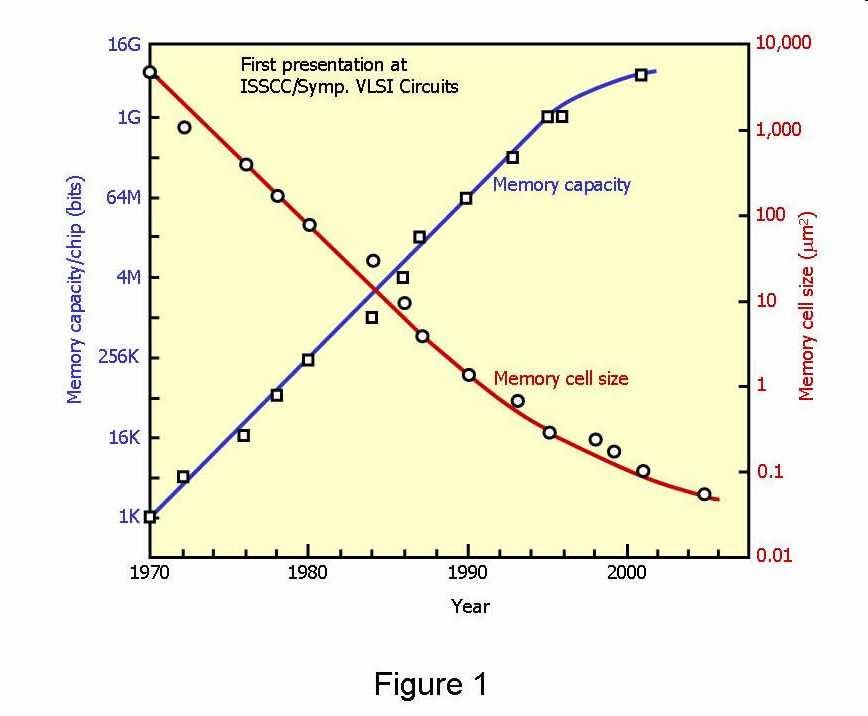
Moores Law for DRAM. 2x increase in capacity every 18 months 2006: 4GB
 MEMORY Moores Law for DRAM 2x increase in capacity every 18 months 2006: 4GB Corollary to Moores Law Cost / chip ~ constant (packaging) Cost / bit = 2X reduction / 18 months Current (2008) ~ 1 micro-cent
Flash Memory Cell Compact Modeling Using PSP Model
 Flash Memory Cell Compact Modeling Using PSP Model Anthony Maure IM2NP Institute UMR CNRS 6137 (Marseille-France) STMicroelectronics (Rousset-France) Outline Motivation Background PSP-Based Flash cell
MTJ-Based Nonvolatile Logic-in-Memory Architecture and Its Application
 2011 11th Non-Volatile Memory Technology Symposium @ Shanghai, China, Nov. 9, 20112 MTJ-Based Nonvolatile Logic-in-Memory Architecture and Its Application Takahiro Hanyu 1,3, S. Matsunaga 1, D. Suzuki
EECS 312: Digital Integrated Circuits Final Exam Solutions 23 April 2009
 Signature: EECS 312: Digital Integrated Circuits Final Exam Solutions 23 April 2009 Robert Dick Show your work. Derivations are required for credit; end results are insufficient. Closed book. You may use
CMOS Inverter. Performance Scaling
 Announcements Exam #2 regrade requests due today. Homework #8 due today. Final Exam: Th June 12, 8:30 10:20am, CMU 120 (extension to 11:20am requested). Grades available for viewing via Catalyst. CMOS
EE141-Fall 2011 Digital Integrated Circuits
 EE4-Fall 20 Digital Integrated Circuits Lecture 5 Memory decoders Administrative Stuff Homework #6 due today Project posted Phase due next Friday Project done in pairs 2 Last Lecture Last lecture Logical
Name: Answers. Mean: 83, Standard Deviation: 12 Q1 Q2 Q3 Q4 Q5 Q6 Total. ESE370 Fall 2015
 University of Pennsylvania Department of Electrical and System Engineering Circuit-Level Modeling, Design, and Optimization for Digital Systems ESE370, Fall 2015 Final Tuesday, December 15 Problem weightings
Topics to be Covered. capacitance inductance transmission lines
 Topics to be Covered Circuit Elements Switching Characteristics Power Dissipation Conductor Sizes Charge Sharing Design Margins Yield resistance capacitance inductance transmission lines Resistance of
Memory, Latches, & Registers
 Memory, Latches, & Registers 1) Structured Logic Arrays 2) Memory Arrays 3) Transparent Latches 4) How to save a few bucks at toll booths 5) Edge-triggered Registers L13 Memory 1 General Table Lookup Synthesis
Introduction to Computer Engineering. CS/ECE 252, Fall 2012 Prof. Guri Sohi Computer Sciences Department University of Wisconsin Madison
 Introduction to Computer Engineering CS/ECE 252, Fall 2012 Prof. Guri Sohi Computer Sciences Department University of Wisconsin Madison Chapter 3 Digital Logic Structures Slides based on set prepared by
University of Toronto. Final Exam
 University of Toronto Final Exam Date - Apr 18, 011 Duration:.5 hrs ECE334 Digital Electronics Lecturer - D. Johns ANSWER QUESTIONS ON THESE SHEETS USING BACKS IF NECESSARY 1. Equation sheet is on last
Random Access Memory. DRAM & SRAM Design DRAM SRAM MS635. Dynamic Random Access Memory. Static Random Access Memory. Cell Structure. 6 Tr.
 DRAM & SRAM Design Random Access Memory Volatile memory Random access is possible if you know the address DRAM DRAM Dynamic Random Access Memory SRAM Static Random Access Memory SRAM Cell Structure Power
Power Dissipation. Where Does Power Go in CMOS?
 Power Dissipation [Adapted from Chapter 5 of Digital Integrated Circuits, 2003, J. Rabaey et al.] Where Does Power Go in CMOS? Dynamic Power Consumption Charging and Discharging Capacitors Short Circuit
L ECE 4211 UConn F. Jain Scaling Laws for NanoFETs Chapter 10 Logic Gate Scaling
 L13 04202017 ECE 4211 UConn F. Jain Scaling Laws for NanoFETs Chapter 10 Logic Gate Scaling Scaling laws: Generalized scaling (GS) p. 610 Design steps p.613 Nanotransistor issues (page 626) Degradation
Objective and Outline. Acknowledgement. Objective: Power Components. Outline: 1) Acknowledgements. Section 4: Power Components
 Acknowledgements. Section 4: Power Components") Objective: Power Components Outline: 1) Acknowledgements 2) Objective and Outline 1 Acknowledgement This lecture note has been obtained from similar courses all over the world. I wish to thank all the
Objective: Power Components Outline: 1) Acknowledgements 2) Objective and Outline 1 Acknowledgement This lecture note has been obtained from similar courses all over the world. I wish to thank all the
Lecture 16: Circuit Pitfalls
 Introduction to CMOS VLSI Design Lecture 16: Circuit Pitfalls David Harris Harvey Mudd College Spring 2004 Outline Pitfalls Detective puzzle Given circuit and symptom, diagnose cause and recommend solution
Dynamic Combinational Circuits. Dynamic Logic
 Dynamic Combinational Circuits Dynamic circuits Charge sharing, charge redistribution Domino logic np-cmos (zipper CMOS) Krish Chakrabarty 1 Dynamic Logic Dynamic gates use a clocked pmos pullup Two modes:
ESE570 Spring University of Pennsylvania Department of Electrical and System Engineering Digital Integrated Cicruits AND VLSI Fundamentals
 University of Pennsylvania Department of Electrical and System Engineering Digital Integrated Cicruits AND VLSI Fundamentals ESE570, Spring 2016 Final Friday, May 6 5 Problems with point weightings shown.
EE141Microelettronica. CMOS Logic
 Microelettronica CMOS Logic CMOS logic Power consumption in CMOS logic gates Where Does Power Go in CMOS? Dynamic Power Consumption Charging and Discharging Capacitors Short Circuit Currents Short Circuit
FERROELECTRIC RAM [FRAM] Submitted in partial fulfillment of the requirement for the award of degree of Bachelor of Technology in Computer Science
![FERROELECTRIC RAM [FRAM] Submitted in partial fulfillment of the requirement for the award of degree of Bachelor of Technology in Computer Science](/thumbs/72/67470194.jpg "FERROELECTRIC RAM [FRAM] Submitted in partial fulfillment of the requirement for the award of degree of Bachelor of Technology in Computer Science") A Seminar report On FERROELECTRIC RAM [FRAM] Submitted in partial fulfillment of the requirement for the award of degree of Bachelor of Technology in Computer Science SUBMITTED TO: www.studymafia.org SUBMITTED
A Seminar report On FERROELECTRIC RAM [FRAM] Submitted in partial fulfillment of the requirement for the award of degree of Bachelor of Technology in Computer Science SUBMITTED TO: www.studymafia.org SUBMITTED
ESE570 Spring University of Pennsylvania Department of Electrical and System Engineering Digital Integrated Cicruits AND VLSI Fundamentals
 University of Pennsylvania Department of Electrical and System Engineering Digital Integrated Cicruits AND VLSI Fundamentals ESE570, Spring 2018 Final Monday, Apr 0 5 Problems with point weightings shown.
F14 Memory Circuits. Lars Ohlsson
 Lars Ohlsson 2018-10-18 F14 Memory Circuits Outline Combinatorial vs. sequential logic circuits Analogue multivibrator circuits Noise in digital circuits CMOS latch CMOS SR flip flop 6T SRAM cell 1T DRAM
3. Design a stick diagram for the PMOS logic shown below [16] Y = (A + B).C. 4. Design a layout diagram for the CMOS logic shown below [16]
![3. Design a stick diagram for the PMOS logic shown below [16] Y = (A + B).C. 4. Design a layout diagram for the CMOS logic shown below [16]](/thumbs/96/128765118.jpg "3. Design a stick diagram for the PMOS logic shown below [16] Y = (A + B).C. 4. Design a layout diagram for the CMOS logic shown below [16]") Code No: RR420203 Set No. 1 1. (a) Find g m and r ds for an n-channel transistor with V GS = 1.2V; V tn = 0.8V; W/L = 10; µncox = 92 µa/v 2 and V DS = Veff + 0.5V The out put impedance constant. λ = 95.3
Code No: RR420203 Set No. 1 1. (a) Find g m and r ds for an n-channel transistor with V GS = 1.2V; V tn = 0.8V; W/L = 10; µncox = 92 µa/v 2 and V DS = Veff + 0.5V The out put impedance constant. λ = 95.3
S No. Questions Bloom s Taxonomy Level UNIT-I
 GROUP-A (SHORT ANSWER QUESTIONS) S No. Questions Bloom s UNIT-I 1 Define oxidation & Classify different types of oxidation Remember 1 2 Explain about Ion implantation Understand 1 3 Describe lithography
CMSC 313 Lecture 25 Registers Memory Organization DRAM
 CMSC 33 Lecture 25 Registers Memory Organization DRAM UMBC, CMSC33, Richard Chang A-75 Four-Bit Register Appendix A: Digital Logic Makes use of tri-state buffers so that multiple registers
ESE570 Spring University of Pennsylvania Department of Electrical and System Engineering Digital Integrated Cicruits AND VLSI Fundamentals
 University of Pennsylvania Department of Electrical and System Engineering Digital Integrated Cicruits AND VLSI Fundamentals ESE570, Spring 017 Final Wednesday, May 3 4 Problems with point weightings shown.
MOSFET: Introduction
 E&CE 437 Integrated VLSI Systems MOS Transistor 1 of 30 MOSFET: Introduction Metal oxide semiconductor field effect transistor (MOSFET) or MOS is widely used for implementing digital designs Its major
CMOS Inverter (static view)
") Review: Design Abstraction Levels SYSTEM CMOS Inverter (static view) + MODULE GATE [Adapted from Chapter 5. 5.3 CIRCUIT of G DEVICE Rabaey s Digital Integrated Circuits,, J. Rabaey et al.] S D Review:
Review: Design Abstraction Levels SYSTEM CMOS Inverter (static view) + MODULE GATE [Adapted from Chapter 5. 5.3 CIRCUIT of G DEVICE Rabaey s Digital Integrated Circuits,, J. Rabaey et al.] S D Review:
ECE251. VLSI System Design
 ECE251. VLSI System Design Project 4 SRAM Cell and Memory Array Operation Area Memory core 4661 mm 2 (256bit) Row Decoder 204.7 mm 2 Collumn Decoder Overall Design Predecoder 156.1 mm 2 Mux 629.2 mm 2
Single Event Effects: SRAM
 Scuola Nazionale di Legnaro 29/3/2007 Single Event Effects: SRAM Alessandro Paccagnella Dipartimento di Ingegneria dell Informazione Università di Padova alessandro.paccagnella@unipd.it OUTLINE Introduction
Lecture 6 Power Zhuo Feng. Z. Feng MTU EE4800 CMOS Digital IC Design & Analysis 2010
 EE4800 CMOS Digital IC Design & Analysis Lecture 6 Power Zhuo Feng 6.1 Outline Power and Energy Dynamic Power Static Power 6.2 Power and Energy Power is drawn from a voltage source attached to the V DD
CS 152 Computer Architecture and Engineering
 CS 152 Computer Architecture and Engineering Lecture 12 VLSI II 2005-2-24 John Lazzaro (www.cs.berkeley.edu/~lazzaro) TAs: Ted Hong and David Marquardt www-inst.eecs.berkeley.edu/~cs152/ Last Time: Device
Lecture 6 NEW TYPES OF MEMORY
 Lecture 6 NEW TYPES OF MEMORY Memory Logic needs memory to function (efficiently) Current memories Volatile memory SRAM DRAM Non-volatile memory (Flash) Emerging memories Phase-change memory STT-MRAM (Ferroelectric
CMPEN 411 VLSI Digital Circuits Spring Lecture 21: Shifters, Decoders, Muxes
 CMPEN 411 VLSI Digital Circuits Spring 2011 Lecture 21: Shifters, Decoders, Muxes [Adapted from Rabaey s Digital Integrated Circuits, Second Edition, 2003 J. Rabaey, A. Chandrakasan, B. Nikolic] Sp11 CMPEN
Gate Carrier Injection and NC-Non- Volatile Memories
 Gate Carrier Injection and NC-Non- Volatile Memories Jean-Pierre Leburton Department of Electrical and Computer Engineering and Beckman Institute University of Illinois at Urbana-Champaign Urbana, IL 61801,
EE 466/586 VLSI Design. Partha Pande School of EECS Washington State University
 EE 466/586 VLSI Design Partha Pande School of EECS Washington State University pande@eecs.wsu.edu Lecture 8 Power Dissipation in CMOS Gates Power in CMOS gates Dynamic Power Capacitance switching Crowbar
Lecture 16: Circuit Pitfalls
 Lecture 16: Circuit Pitfalls Outline Variation Noise Budgets Reliability Circuit Pitfalls 2 Variation Process Threshold Channel length Interconnect dimensions Environment Voltage Temperature Aging / Wearout
Dynamic Combinational Circuits. Dynamic Logic
 Dynamic Combinational Circuits Dynamic circuits Charge sharing, charge redistribution Domino logic np-cmos (zipper CMOS) Krish Chakrabarty 1 Dynamic Logic Dynamic gates use a clocked pmos pullup Two modes:
Lecture 24. CMOS Logic Gates and Digital VLSI II
 ecture 24 CMOS ogic Gates and Digital VSI II In this lecture you will learn: Static CMOS ogic Gates FET Scaling CMOS Memory, SRM and DRM CMOS atches, and Registers (Flip-Flops) Clocked CMOS CCDs CMOS ogic:
Advanced Flash and Nano-Floating Gate Memories
 Advanced Flash and Nano-Floating Gate Memories Mater. Res. Soc. Symp. Proc. Vol. 1337 2011 Materials Research Society DOI: 10.1557/opl.2011.1028 Scaling Challenges for NAND and Replacement Memory Technology
Chapter 3 Basics Semiconductor Devices and Processing
 Chapter 3 Basics Semiconductor Devices and Processing Hong Xiao, Ph. D. www2.austin.cc.tx.us/hongxiao/book.htm Hong Xiao, Ph. D. www2.austin.cc.tx.us/hongxiao/book.htm 1 Objectives Identify at least two
LH5P832. CMOS 256K (32K 8) Pseudo-Static RAM
 Pseudo-Static RAM") LH5P832 CMOS 256K (32K 8) Pseudo-Static RAM FEATURES 32,768 8 bit organization Access time: 100/120 ns (MAX.) Cycle time: 160/190 ns (MIN.) Power consumption: Operating: 357.5/303 mw Standby: 16.5 mw TTL
LH5P832 CMOS 256K (32K 8) Pseudo-Static RAM FEATURES 32,768 8 bit organization Access time: 100/120 ns (MAX.) Cycle time: 160/190 ns (MIN.) Power consumption: Operating: 357.5/303 mw Standby: 16.5 mw TTL
WARM SRAM: A Novel Scheme to Reduce Static Leakage Energy in SRAM Arrays
 WARM SRAM: A Novel Scheme to Reduce Static Leakage Energy in SRAM Arrays Mahadevan Gomathisankaran Iowa State University gmdev@iastate.edu Akhilesh Tyagi Iowa State University tyagi@iastate.edu ➀ Introduction
Chapter 7. Sequential Circuits Registers, Counters, RAM
 Chapter 7. Sequential Circuits Registers, Counters, RAM Register - a group of binary storage elements suitable for holding binary info A group of FFs constitutes a register Commonly used as temporary storage
CMPEN 411 VLSI Digital Circuits. Lecture 04: CMOS Inverter (static view)
") CMPEN 411 VLSI Digital Circuits Lecture 04: CMOS Inverter (static view) Kyusun Choi [Adapted from Rabaey s Digital Integrated Circuits, Second Edition, 2003 J. Rabaey, A. Chandrakasan, B. Nikolic] CMPEN
CMPEN 411 VLSI Digital Circuits Lecture 04: CMOS Inverter (static view) Kyusun Choi [Adapted from Rabaey s Digital Integrated Circuits, Second Edition, 2003 J. Rabaey, A. Chandrakasan, B. Nikolic] CMPEN
CMOS Transistors, Gates, and Wires
 CMOS Transistors, Gates, and Wires Should the hardware abstraction layers make today s lecture irrelevant? pplication R P C W / R W C W / 6.375 Complex Digital Systems Christopher atten February 5, 006
Floating Gate Devices: Operation and Compact Modeling
 Floating Gate Devices: Operation and Compact Modeling Paolo Pavan (1), Luca Larcher (1) and Andrea MarmirolI (2) (1) Università di Modena e Reggio Emilia, Via Fogliani, 1 42100 Reggio Emilia (Italy) -
Chapter 2 CMOS Transistor Theory. Jin-Fu Li Department of Electrical Engineering National Central University Jungli, Taiwan
 Chapter 2 CMOS Transistor Theory Jin-Fu Li Department of Electrical Engineering National Central University Jungli, Taiwan Outline Introduction MOS Device Design Equation Pass Transistor Jin-Fu Li, EE,
ELEN0037 Microelectronic IC Design. Prof. Dr. Michael Kraft
 ELEN0037 Microelectronic IC Design Prof. Dr. Michael Kraft Lecture 2: Technological Aspects Technology Passive components Active components CMOS Process Basic Layout Scaling CMOS Technology Integrated
N ano scale l S il ii lco i n B ased N o nvo lat l i atl ie l M em ory r Chungwoo Kim, Ph.D.
 cw_kim@samsung.com Acknowledgements Collaboration Funding Outline Introduction Current research status Nano fabrication Process Nanoscale patterning SiN thin film Si Nanoparticle Nano devices Nanoscale
Digital Integrated Circuits Lecture 14: CAMs, ROMs, and PLAs
 Digital Integrated Circuits Lecture 4: CAMs, ROMs, and PLAs Chih-Wei Liu VLSI Signal Processing LAB National Chiao Tung University cwliu@twins.ee.nctu.edu.tw DIC-Lec4 cwliu@twins.ee.nctu.edu.tw Outline
Introduction to Computer Engineering. CS/ECE 252, Spring 2017 Rahul Nayar Computer Sciences Department University of Wisconsin Madison
 Introduction to Computer Engineering CS/ECE 252, Spring 2017 Rahul Nayar Computer Sciences Department University of Wisconsin Madison Chapter 3 Digital Logic Structures Slides based on set prepared by
ECE 438: Digital Integrated Circuits Assignment #4 Solution The Inverter
 ECE 438: Digital Integrated Circuits Assignment #4 The Inverter Text: Chapter 5, Digital Integrated Circuits 2 nd Ed, Rabaey 1) Consider the CMOS inverter circuit in Figure P1 with the following parameters.
LH5P8128. CMOS 1M (128K 8) Pseudo-Static RAM PIN CONNECTIONS
 Pseudo-Static RAM PIN CONNECTIONS") LH5P8128 FEATURES 131,072 8 bit organization Access times (MAX.): 60/80/100 ns Cycle times (MIN.): 100/130/160 ns Single +5 V power supply Power consumption: Operating: 572/385/275 mw (MAX.) Standby (CMOS
LH5P8128 FEATURES 131,072 8 bit organization Access times (MAX.): 60/80/100 ns Cycle times (MIN.): 100/130/160 ns Single +5 V power supply Power consumption: Operating: 572/385/275 mw (MAX.) Standby (CMOS
Pass-Transistor Logic
 -all 26 Digital tegrated ircuits nnouncements No new homework this week roject phase one due on Monday Midterm 2 next Thursday Review session on Tuesday Lecture 8 Logic Dynamic Logic EE4 EE4 2 lass Material
Spiral 2 7. Capacitance, Delay and Sizing. Mark Redekopp
 2-7.1 Spiral 2 7 Capacitance, Delay and Sizing Mark Redekopp 2-7.2 Learning Outcomes I understand the sources of capacitance in CMOS circuits I understand how delay scales with resistance, capacitance
The Physical Structure (NMOS)
") The Physical Structure (NMOS) Al SiO2 Field Oxide Gate oxide S n+ Polysilicon Gate Al SiO2 SiO2 D n+ L channel P Substrate Field Oxide contact Metal (S) n+ (G) L W n+ (D) Poly 1 Transistor Resistance Two
The Physical Structure (NMOS) Al SiO2 Field Oxide Gate oxide S n+ Polysilicon Gate Al SiO2 SiO2 D n+ L channel P Substrate Field Oxide contact Metal (S) n+ (G) L W n+ (D) Poly 1 Transistor Resistance Two
High-to-Low Propagation Delay t PHL
 High-to-Low Propagation Delay t PHL V IN switches instantly from low to high. Driver transistor (n-channel) immediately switches from cutoff to saturation; the p-channel pull-up switches from triode to
C.K. Ken Yang UCLA Courtesy of MAH EE 215B
 Decoders: Logical Effort Applied C.K. Ken Yang UCLA yang@ee.ucla.edu Courtesy of MAH 1 Overview Reading Rabaey 6.2.2 (Ratio-ed logic) W&H 6.2.2 Overview We have now gone through the basics of decoders,
EECS 141 F01 Lecture 17
 EECS 4 F0 Lecture 7 With major inputs/improvements From Mary-Jane Irwin (Penn State) Dynamic CMOS In static circuits at every point in time (except when switching) the output is connected to either GND
MOS Transistor Theory
 CHAPTER 3 MOS Transistor Theory Outline 2 1. Introduction 2. Ideal I-V Characteristics 3. Nonideal I-V Effects 4. C-V Characteristics 5. DC Transfer Characteristics 6. Switch-level RC Delay Models MOS
MOS Transistor I-V Characteristics and Parasitics
 ECEN454 Digital Integrated Circuit Design MOS Transistor I-V Characteristics and Parasitics ECEN 454 Facts about Transistors So far, we have treated transistors as ideal switches An ON transistor passes
VLSI GATE LEVEL DESIGN UNIT - III P.VIDYA SAGAR ( ASSOCIATE PROFESSOR) Department of Electronics and Communication Engineering, VBIT
 Department of Electronics and Communication Engineering, VBIT") VLSI UNIT - III GATE LEVEL DESIGN P.VIDYA SAGAR ( ASSOCIATE PROFESSOR) contents GATE LEVEL DESIGN : Logic Gates and Other complex gates, Switch logic, Alternate gate circuits, Time Delays, Driving large
VLSI UNIT - III GATE LEVEL DESIGN P.VIDYA SAGAR ( ASSOCIATE PROFESSOR) contents GATE LEVEL DESIGN : Logic Gates and Other complex gates, Switch logic, Alternate gate circuits, Time Delays, Driving large
ENGR890 Digital VLSI Design Fall Lecture 4: CMOS Inverter (static view)
") ENGR89 Digital VLSI Design Fall 5 Lecture 4: CMOS Inverter (static view) [Adapted from Chapter 5 of Digital Integrated Circuits, 3, J. Rabaey et al.] [Also borrowed from Vijay Narayanan and Mary Jane Irwin]
ENGR89 Digital VLSI Design Fall 5 Lecture 4: CMOS Inverter (static view) [Adapted from Chapter 5 of Digital Integrated Circuits, 3, J. Rabaey et al.] [Also borrowed from Vijay Narayanan and Mary Jane Irwin]
Lecture 23. Dealing with Interconnect. Impact of Interconnect Parasitics
 Lecture 23 Dealing with Interconnect Impact of Interconnect Parasitics Reduce Reliability Affect Performance Classes of Parasitics Capacitive Resistive Inductive 1 INTERCONNECT Dealing with Capacitance
THE INVERTER. Inverter
 THE INVERTER DIGITAL GATES Fundamental Parameters Functionality Reliability, Robustness Area Performance» Speed (delay)» Power Consumption» Energy Noise in Digital Integrated Circuits v(t) V DD i(t) (a)
Floating Point Representation and Digital Logic. Lecture 11 CS301
 Floating Point Representation and Digital Logic Lecture 11 CS301 Administrative Daily Review of today s lecture w Due tomorrow (10/4) at 8am Lab #3 due Friday (9/7) 1:29pm HW #5 assigned w Due Monday 10/8
ESE 570: Digital Integrated Circuits and VLSI Fundamentals
 ESE 570: Digital Integrated Circuits and VLSI Fundamentals Lec 18: March 27, 2018 Dynamic Logic, Charge Injection Lecture Outline! Sequential MOS Logic " D-Latch " Timing Constraints! Dynamic Logic " Domino
Section 3: Combinational Logic Design. Department of Electrical Engineering, University of Waterloo. Combinational Logic
 Section 3: Combinational Logic Design Major Topics Design Procedure Multilevel circuits Design with XOR gates Adders and Subtractors Binary parallel adder Decoders Encoders Multiplexers Programmed Logic
MOS Transistor Properties Review
 MOS Transistor Properties Review 1 VLSI Chip Manufacturing Process Photolithography: transfer of mask patterns to the chip Diffusion or ion implantation: selective doping of Si substrate Oxidation: SiO
EE115C Winter 2017 Digital Electronic Circuits. Lecture 3: MOS RC Model, CMOS Manufacturing
 EE115C Winter 2017 Digital Electronic Circuits Lecture 3: MOS RC Model, CMOS Manufacturing Agenda MOS Transistor: RC Model (pp. 104-113) S R on D CMOS Manufacturing Process (pp. 36-46) S S C GS G G C GD
Software Engineering 2DA4. Slides 8: Multiplexors and More
 Software Engineering 2DA4 Slides 8: Multiplexors and More Dr. Ryan Leduc Department of Computing and Software McMaster University Material based on S. Brown and Z. Vranesic, Fundamentals of Digital Logic