Semiconductor Memories
|
|
|
- Domenic Washington
- 5 years ago
- Views:
Transcription


1 !"#"$%&'()$*#+%$*,' -"+./"$0 1'!*0"#)'2*+03*.$"4* Jan M. Rabaey Anantha Chandrakasan Borivoje Nikolic Semiconductor Memories December 20, 2002
2 !"#$%&'()*&'*+&, Memory Classification Memory Architectures The Memory Core Periphery Reliability Case Studies
3 !"#$%&'()%*&+,-"#&+.,/0122$3$%1*$&' Read-W rite M emory Non-Volatile Read-W rite Memory Read-Only Memory Random Access Non-Random Access EPROM E 2 PROM Mask-Programmed Programmable (PROM) SRAM FIFO FLASH DRAM LIFO Shift Register CAM
4 !"#$%&'()#)*+,'-".)*)/)$*0
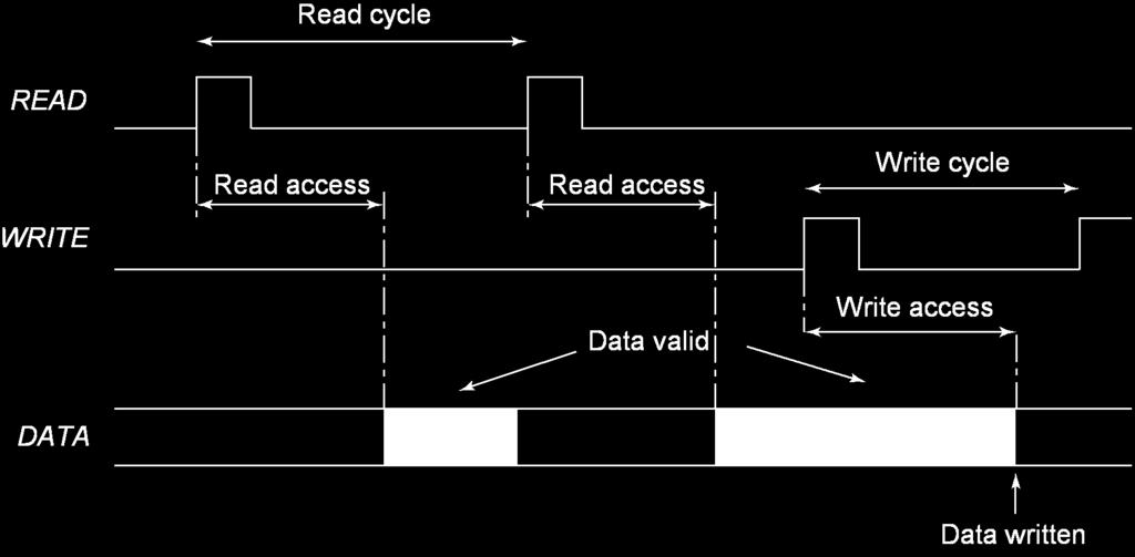
5 !"#$%&'(%)*+,"),-%".'/")$0"%1 M bits M bits S 0 S 1 S 2 Word 0 Word 1 Word 2 Storage cell A 0 A 1 S 0 Word 0 Word 1 Word 2 Storage cell words N S N 2 2 WordN2 2 A K 2 1 Decoder WordN2 2 S N 2 1 WordN2 1 K 5 log 2 N WordN2 1 Input-Output (M bits) Input-Output (M bits) Intuitive architecture for N x M memory Too many select signals: N words == N select signals Decoder reduces the number of select signals K = log 2 N
01'*)'(\"* Problem: ASPECT RATIO or HEIGHT >> WIDTH Amplify swing to")
6 !""#$%&'"()'("*+,-*./"$,!")01'*)'("* Problem: ASPECT RATIO or HEIGHT >> WIDTH Amplify swing to rail-to-rail amplitude Selects appropriate word


7 !"#$%$&'"&%()*#+,$-).$&'"/#&/0$# Advantages: 1. Shorter wires within blocks 2. Block address activates only 1 block => power savings

8 !"#$%&'()#)*+,'-..%$/01"2 DRAM Timing Multiplexed Adressing SRAM Timing Self-timed
9 !"#$%&'()*+",-.)*/"((0 BL BL BL 1 WL WL V DD WL BL BL BL 0 WL WL WL GND Diode ROM MOS ROM 1 MOS ROM 2
10 !"#$%"&$&"! V DD Pull-up devices WL[0] GND WL [1] WL [2] GND WL [3] BL [0] BL [1] BL [2] BL [3]
11 !"#$%"&$&"!$'()*+, Cell (9.5 x 7 ) Programmming using the Active Layer Only Polysilicon Metal1 Diffusion Metal1 on Diffusion
12 !"#$%&%'$("! V DD Pull-up devices BL[0] BL[1] BL[2] BL[3] WL[0] WL[1] WL[2] WL[3] All word lines high by default with exception of selected row
13 !"#$%&%'$("!$)*+,-. Cell (8 x 7 ) Programmming using the Metal-1 Layer Only No contact to VDD or GND necessary; drastically reduced cell size Loss in performance compared to NOR ROM Polysilicon Diffusion Metal1 on Diffusion
14 !"!#$%&'$()*+,- Cell (5 x 6 ) Programmming using Implants O nly Polysilicon Threshold-altering implant Metal1 on Diffusion
15 !"#$"%&'()*+,$-*.'("*!"/%0 WL Driver Polysilicon word line Metal word line (a) Driving the word line from both sides Metal bypass WL K cells (b) Using a metal bypass Polysilicon word line (c) Use silicides
16 !"#$%&"'#()*+,)-+.).+* f pre V DD Precharge devices WL [0] WL [1] GND WL [2] GND WL [3] BL [0] BL [1] BL [2] BL [3] PMOS precharge device can be made as large as necessary, but clock driver becomes harder to design.
/(\".")

17 !"#$%"&'()&*+,*-".)*/ 01*+2&"'()#3$3'(*+(.'#/)/(".+425,678 Source Floating gate Gate Drain D t ox G n + Substrate p t ox n +_ S Device cross-section Schematic symbol

18 !"#$%&'()*$%+,-.$'/&/%#.,0.#(.$11&'( 20 V 0 V 5 V 10 V 5 V 20 V 2 5 V 0 V V 5 V S D S D S D Avalanche injection Removing programming voltage leaves charge trapped Programming results in higher V T.
19 !
20 !"#$#%&''()#* Floating gate Source Gate Drain I nm n 1 Substrate p n 1 10 nm -10 V 10 V V GD FLOTOX transistor Fowler-Nordheim I-V characteristic

21 !!"#$%&'()) BL WL V DD Absolute threshold control is hard Unprogrammed transistor might be depletion 2 transistor cell
22 !"#$%&''()*+ Control gate Floating gate erasure n 1 source programming p- substrate Thin tunneling oxide n 1 drain
23 !"#$%
24 !"#$%

25 !"#$
 Unit Cell Gate ONO Gate Oxide FG")
26 !"!#$%&'()$*+,-./ Word line(poly) Unit Cell Gate ONO Gate Oxide FG Source line (Diff. Layer) Courtesy Toshiba
27 !"!#$%&'()$*+,-./ Select transistor Word lines Active area ST I Bit line contact Source line contact Courtesy Toshiba


28 !"#$#%&'$()&(%)*+,*-&#&'.+,.&"'.#$&*/01
29 !"#$%&'()"*+",-'(".*/!0+1 STATIC (SRAM) Data stored as long as supply is applied Large (6 transistors/cell) Fast Differential DYNAMIC (DRAM) Periodic refresh required Small (1-3 transistors/cell) Slower Single Ended
30 !"#$%&'('#)$*+,-.*./0,*+122* WL V DD M 2 M 4 Q M Q M 5 6 M 1 M 3 BL BL
*+,-.")


31 !"#$%&'( )*+,-.( V DD M2 M4 Q Q M1 M3 M5 M6 GND WL BL BL

32 !"#$#%&'(")*+&,-.!/0-1"** V DD WL R L R L M 3 Q Q M 4 BL M 1 M 2 BL Static power dissipation -- Want R L large Bit lines precharged to V DD to address t p problem
33 !"#$%&'()(*+,)-.+-*.

34 !"#$%&'(')*$+,-./+0122 Write: C S is charged or discharged by asserting WL and BL. Read: Charge redistribution takes places between bit line and storage capacitance V = VBL V PRE = V BIT V PRE C S C S C BL Voltage swing is small; typically around 250 mv.
35 !"#$%&'((%)*+',-./012+ 1T DRAM requires a sense amplifier for each bit line, due to charge redistribution read-out. DRAM memory cells are single ended in contrast to SRAM cells. The read-out of the 1T DRAM cell is destructive; read and refresh operations are necessary for correct operation. Unlike 3T cell, 1T cell requires presence of an extra capacitance that must be explicitly included in the design. 1 is lost. This charge loss can be circumvented by bootstrapping the word lines to a higher value than V DD
36 !"#$"%&'(%)("*+,-.# V BL V(1) V PRE DV(1) Sense amp activated Word line activated V(0) t

37 !"#$%&'($)*++ Capacitor Metal word line Poly n + n + Inversion layer Poly induced by plate bias Cross-section SiO 2 Field Oxide Diffused bit line Polysilicon gate Layout Polysilicon plate M 1 word line Uses Polysilicon-Diffusion Capacitance Expensive in Area

38 !"#$%&"#' Decoders Sense Amplifiers Input/Output Buffers Control / Timing Circuitry
39 !"#$%&'"(&)* Collection of 2 M complex logic gates Organized in regular and dense fashion (N)AND Decoder NOR Decoder
40 !"#$%$&'"&%()*#&+,#$- Multi-stage implementation improves performance WL 1 WL 0 A 0 A 1 A 0 A 1 A 0 A 1 A 0 A 1 A 2 A 3 A 2 A 3 A 2 A 3 A 2 A 3 A 1 A 0 A 0 A 1 A 3 A 2 A 2 A 3 NAND decoder using 2-input pre-decoders
41 !"#$%&'(!)'*+),- Precharge devices GND GND V DD WL 3 V DD WL 3 WL 2 V DD WL 2 WL 1 WL 0 V DD WL 1 WL 0 V DD A 0 A 0 A 1 A 1 A 0 A 0 A 1 A 1 2-input NOR decoder 2-input NAND decoder

 Only one extra transistor in signal path")
42 !"#$%&'(%)**"'+)$*#*',+(-)*./(0,1&2$( /.0,/.+ BL 0 BL 1 BL 2 BL 3 A 0 S 0 S 1 S 2 A 1 S 3 2-input NOR decoder Advantages: speed (t pd does not add to overall memory access time) Only one extra transistor in signal path Disadvantage: Large transistor count D
GMU, ECE 680 Physical VLSI Design 1
 ECE680: Physical VLSI Design Chapter VIII Semiconductor Memory (chapter 12 in textbook) 1 Chapter Overview Memory Classification Memory Architectures The Memory Core Periphery Reliability Case Studies
Digital Integrated Circuits A Design Perspective
 Semiconductor Memories Adapted from Chapter 12 of Digital Integrated Circuits A Design Perspective Jan M. Rabaey et al. Copyright 2003 Prentice Hall/Pearson Outline Memory Classification Memory Architectures
Semiconductor Memory Classification
 Semiconductor Memory Classification Read-Write Memory Non-Volatile Read-Write Memory Read-Only Memory Random Access Non-Random Access EPROM E 2 PROM Mask-Programmed Programmable (PROM) SRAM FIFO FLASH
Lecture 25. Semiconductor Memories. Issues in Memory
 Lecture 25 Semiconductor Memories Issues in Memory Memory Classification Memory Architectures TheMemoryCore Periphery 1 Semiconductor Memory Classification RWM NVRWM ROM Random Access Non-Random Access
Digital Integrated Circuits A Design Perspective. Semiconductor. Memories. Memories
 Digital Integrated Circuits A Design Perspective Semiconductor Chapter Overview Memory Classification Memory Architectures The Memory Core Periphery Reliability Case Studies Semiconductor Memory Classification
Semiconductor Memories
 Semiconductor References: Adapted from: Digital Integrated Circuits: A Design Perspective, J. Rabaey UCB Principles of CMOS VLSI Design: A Systems Perspective, 2nd Ed., N. H. E. Weste and K. Eshraghian
SEMICONDUCTOR MEMORIES
 SEMICONDUCTOR MEMORIES Semiconductor Memory Classification RWM NVRWM ROM Random Access Non-Random Access EPROM E 2 PROM Mask-Programmed Programmable (PROM) SRAM FIFO FLASH DRAM LIFO Shift Register CAM
Magnetic core memory (1951) cm 2 ( bit)
 cm 2 ( bit)") Magnetic core memory (1951) 16 16 cm 2 (128 128 bit) Semiconductor Memory Classification Read-Write Memory Non-Volatile Read-Write Memory Read-Only Memory Random Access Non-Random Access EPROM E 2 PROM
Magnetic core memory (1951) 16 16 cm 2 (128 128 bit) Semiconductor Memory Classification Read-Write Memory Non-Volatile Read-Write Memory Read-Only Memory Random Access Non-Random Access EPROM E 2 PROM
Hw 6 and 7 Graded and available Project Phase 2 Graded Project Phase 3 Launch Today
 EECS141 1 Hw 8 Posted Last one to be graded Due Friday April 30 Hw 6 and 7 Graded and available Project Phase 2 Graded Project Phase 3 Launch Today EECS141 2 1 6 5 4 3 2 1 0 1.5 2 2.5 3 3.5 4 Frequency
Semiconductor memories
 Semiconductor memories Semiconductor Memories Data in Write Memory cell Read Data out Some design issues : How many cells? Function? Power consuption? Access type? How fast are read/write operations? Semiconductor
Semiconductor Memories
 Digital Integrated Circuits A Design Perspective Jan M. Rabaey Anantha Chandrakasan Borivoje Nikolic Semiconductor Memories December 20, 2002 Chapter Overview Memory Classification Memory Architectures
EE141- Fall 2002 Lecture 27. Memory EE141. Announcements. We finished all the labs No homework this week Projects are due next Tuesday 9am EE141
 - Fall 2002 Lecture 27 Memory Announcements We finished all the labs No homework this week Projects are due next Tuesday 9am 1 Today s Lecture Memory:» SRAM» DRAM» Flash Memory 2 Floating-gate transistor
EE241 - Spring 2000 Advanced Digital Integrated Circuits. References
 EE241 - Spring 2000 Advanced Digital Integrated Circuits Lecture 26 Memory References Rabaey, Digital Integrated Circuits Memory Design and Evolution, VLSI Circuits Short Course, 1998.» Gillingham, Evolution
Semiconductor Memories. Jan M. Rabaey Anantha Chandrakasan Borivoje Nikolic Paolo Spirito
 Semiconductor Memories Jan M. Rabaey Anantha Chandrakasan Borivoje Nikolic Paolo Spirito Memory Classification Memory Classification Read-Write Memory Non-Volatile Read-Write Memory Read-Only Memory Random
Chapter Overview. Memory Classification. Memory Architectures. The Memory Core. Periphery. Reliability. Memory
 SRAM Design Chapter Overview Classification Architectures The Core Periphery Reliability Semiconductor Classification RWM NVRWM ROM Random Access Non-Random Access EPROM E 2 PROM Mask-Programmed Programmable
ESE 570: Digital Integrated Circuits and VLSI Fundamentals
 ESE 570: Digital Integrated Circuits and VLSI Fundamentals Lec 21: April 4, 2017 Memory Overview, Memory Core Cells Penn ESE 570 Spring 2017 Khanna Today! Memory " Classification " ROM Memories " RAM Memory
Semiconductor Memories
 Digital Integrated Circuits A Design Perspective Jan M. Rabaey Anantha Chandrakasan Borivoje Nikolic Semiconductor Memories December 20, 2002 Chapter Overview Memory Classification Memory Architectures
Memory Trend. Memory Architectures The Memory Core Periphery
 Semiconductor Memories: an Introduction ti Talk Overview Memory Trend Memory Classification Memory Architectures The Memory Core Periphery Reliability Semiconductor Memory Trends (up to the 90 s) Memory
Topics. Dynamic CMOS Sequential Design Memory and Control. John A. Chandy Dept. of Electrical and Computer Engineering University of Connecticut
 Topics Dynamic CMOS Sequential Design Memory and Control Dynamic CMOS In static circuits at every point in time (except when switching) the output is connected to either GND or V DD via a low resistance
ESE 570: Digital Integrated Circuits and VLSI Fundamentals
 ESE 570: Digital Integrated Circuits and VLSI Fundamentals Lec 19: March 29, 2018 Memory Overview, Memory Core Cells Today! Charge Leakage/Charge Sharing " Domino Logic Design Considerations! Logic Comparisons!
EE141. EE141-Spring 2006 Digital Integrated Circuits. Administrative Stuff. Class Material. Flash Memory. Read-Only Memory Cells MOS OR ROM
 EE141-pring 2006 igital Integrated Circuits Lecture 29 Flash memory Administrative tuff reat job on projects and posters! Homework #10 due today Lab reports due this week Friday lab in 353 Final exam May
! Charge Leakage/Charge Sharing. " Domino Logic Design Considerations. ! Logic Comparisons. ! Memory. " Classification. " ROM Memories.
 ESE 57: Digital Integrated Circuits and VLSI Fundamentals Lec 9: March 9, 8 Memory Overview, Memory Core Cells Today! Charge Leakage/ " Domino Logic Design Considerations! Logic Comparisons! Memory " Classification
Semiconductor Memories
 Introduction Classification of Memory Devices "Combinational Logic" Read Write Memories Non Volatile RWM Read Only Memory Random Access Non-Random Access Static RAM FIFO Dynamic RAM LIFO Shift Register
! Memory. " RAM Memory. ! Cell size accounts for most of memory array size. ! 6T SRAM Cell. " Used in most commercial chips
 ESE 57: Digital Integrated Circuits and VLSI Fundamentals Lec : April 3, 8 Memory: Core Cells Today! Memory " RAM Memory " Architecture " Memory core " SRAM " DRAM " Periphery Penn ESE 57 Spring 8 - Khanna
Administrative Stuff
 EE141- Spring 2004 Digital Integrated Circuits Lecture 30 PERSPECTIVES 1 Administrative Stuff Homework 10 posted just for practice. No need to turn in (hw 9 due today). Normal office hours next week. HKN
ECE520 VLSI Design. Lecture 23: SRAM & DRAM Memories. Payman Zarkesh-Ha
 ECE520 VLSI Design Lecture 23: SRAM & DRAM Memories Payman Zarkesh-Ha Office: ECE Bldg. 230B Office hours: Wednesday 2:00-3:00PM or by appointment E-mail: pzarkesh@unm.edu Slide: 1 Review of Last Lecture
CMOS Digital Integrated Circuits Lec 13 Semiconductor Memories
 Lec 13 Semiconductor Memories 1 Semiconductor Memory Types Semiconductor Memories Read/Write (R/W) Memory or Random Access Memory (RAM) Read-Only Memory (ROM) Dynamic RAM (DRAM) Static RAM (SRAM) 1. Mask
The Devices. Digital Integrated Circuits A Design Perspective. Jan M. Rabaey Anantha Chandrakasan Borivoje Nikolic. July 30, 2002
 Digital Integrated Circuits A Design Perspective Jan M. Rabaey Anantha Chandrakasan Borivoje Nikolic The Devices July 30, 2002 Goal of this chapter Present intuitive understanding of device operation Introduction
CMPEN 411 VLSI Digital Circuits Spring Lecture 21: Shifters, Decoders, Muxes
 CMPEN 411 VLSI Digital Circuits Spring 2011 Lecture 21: Shifters, Decoders, Muxes [Adapted from Rabaey s Digital Integrated Circuits, Second Edition, 2003 J. Rabaey, A. Chandrakasan, B. Nikolic] Sp11 CMPEN
EECS 312: Digital Integrated Circuits Final Exam Solutions 23 April 2009
 Signature: EECS 312: Digital Integrated Circuits Final Exam Solutions 23 April 2009 Robert Dick Show your work. Derivations are required for credit; end results are insufficient. Closed book. You may use
EE141-Fall 2011 Digital Integrated Circuits
 EE4-Fall 20 Digital Integrated Circuits Lecture 5 Memory decoders Administrative Stuff Homework #6 due today Project posted Phase due next Friday Project done in pairs 2 Last Lecture Last lecture Logical
Thin Film Transistors (TFT)
") Thin Film Transistors (TFT) a-si TFT - α-si:h (Hydrogenated amorphous Si) deposited with a PECVD system (low temp. process) replaces the single crystal Si substrate. - Inverted staggered structure with
Thin Film Transistors (TFT) a-si TFT - α-si:h (Hydrogenated amorphous Si) deposited with a PECVD system (low temp. process) replaces the single crystal Si substrate. - Inverted staggered structure with
Moores Law for DRAM. 2x increase in capacity every 18 months 2006: 4GB
 MEMORY Moores Law for DRAM 2x increase in capacity every 18 months 2006: 4GB Corollary to Moores Law Cost / chip ~ constant (packaging) Cost / bit = 2X reduction / 18 months Current (2008) ~ 1 micro-cent
Name: Answers. Mean: 83, Standard Deviation: 12 Q1 Q2 Q3 Q4 Q5 Q6 Total. ESE370 Fall 2015
 University of Pennsylvania Department of Electrical and System Engineering Circuit-Level Modeling, Design, and Optimization for Digital Systems ESE370, Fall 2015 Final Tuesday, December 15 Problem weightings
Flash Memory Cell Compact Modeling Using PSP Model
 Flash Memory Cell Compact Modeling Using PSP Model Anthony Maure IM2NP Institute UMR CNRS 6137 (Marseille-France) STMicroelectronics (Rousset-France) Outline Motivation Background PSP-Based Flash cell
University of Toronto. Final Exam
 University of Toronto Final Exam Date - Apr 18, 011 Duration:.5 hrs ECE334 Digital Electronics Lecturer - D. Johns ANSWER QUESTIONS ON THESE SHEETS USING BACKS IF NECESSARY 1. Equation sheet is on last
Digital Integrated Circuits A Design Perspective. Jan M. Rabaey Anantha Chandrakasan Borivoje Nikolic. The Devices. July 30, Devices.
 Digital Integrated Circuits A Design Perspective Jan M. Rabaey Anantha Chandrakasan Borivoje Nikolic The July 30, 2002 1 Goal of this chapter Present intuitive understanding of device operation Introduction
Dynamic Combinational Circuits. Dynamic Logic
 Dynamic Combinational Circuits Dynamic circuits Charge sharing, charge redistribution Domino logic np-cmos (zipper CMOS) Krish Chakrabarty 1 Dynamic Logic Dynamic gates use a clocked pmos pullup Two modes:
S No. Questions Bloom s Taxonomy Level UNIT-I
 GROUP-A (SHORT ANSWER QUESTIONS) S No. Questions Bloom s UNIT-I 1 Define oxidation & Classify different types of oxidation Remember 1 2 Explain about Ion implantation Understand 1 3 Describe lithography
Dynamic Combinational Circuits. Dynamic Logic
 Dynamic Combinational Circuits Dynamic circuits Charge sharing, charge redistribution Domino logic np-cmos (zipper CMOS) Krish Chakrabarty 1 Dynamic Logic Dynamic gates use a clocked pmos pullup Two modes:
Power Dissipation. Where Does Power Go in CMOS?
 Power Dissipation [Adapted from Chapter 5 of Digital Integrated Circuits, 2003, J. Rabaey et al.] Where Does Power Go in CMOS? Dynamic Power Consumption Charging and Discharging Capacitors Short Circuit
Fig. 1 CMOS Transistor Circuits (a) Inverter Out = NOT In, (b) NOR-gate C = NOT (A or B)
 Inverter Out = NOT In, (b) NOR-gate C = NOT (A or B)") 1 Introduction to Transistor-Level Logic Circuits 1 By Prawat Nagvajara At the transistor level of logic circuits, transistors operate as switches with the logic variables controlling the open or closed
1 Introduction to Transistor-Level Logic Circuits 1 By Prawat Nagvajara At the transistor level of logic circuits, transistors operate as switches with the logic variables controlling the open or closed
CMOS Inverter (static view)
") Review: Design Abstraction Levels SYSTEM CMOS Inverter (static view) + MODULE GATE [Adapted from Chapter 5. 5.3 CIRCUIT of G DEVICE Rabaey s Digital Integrated Circuits,, J. Rabaey et al.] S D Review:
Review: Design Abstraction Levels SYSTEM CMOS Inverter (static view) + MODULE GATE [Adapted from Chapter 5. 5.3 CIRCUIT of G DEVICE Rabaey s Digital Integrated Circuits,, J. Rabaey et al.] S D Review:
Spiral 2 7. Capacitance, Delay and Sizing. Mark Redekopp
 2-7.1 Spiral 2 7 Capacitance, Delay and Sizing Mark Redekopp 2-7.2 Learning Outcomes I understand the sources of capacitance in CMOS circuits I understand how delay scales with resistance, capacitance
MOSFET: Introduction
 E&CE 437 Integrated VLSI Systems MOS Transistor 1 of 30 MOSFET: Introduction Metal oxide semiconductor field effect transistor (MOSFET) or MOS is widely used for implementing digital designs Its major
L ECE 4211 UConn F. Jain Scaling Laws for NanoFETs Chapter 10 Logic Gate Scaling
 L13 04202017 ECE 4211 UConn F. Jain Scaling Laws for NanoFETs Chapter 10 Logic Gate Scaling Scaling laws: Generalized scaling (GS) p. 610 Design steps p.613 Nanotransistor issues (page 626) Degradation
EE141Microelettronica. CMOS Logic
 Microelettronica CMOS Logic CMOS logic Power consumption in CMOS logic gates Where Does Power Go in CMOS? Dynamic Power Consumption Charging and Discharging Capacitors Short Circuit Currents Short Circuit
Memory, Latches, & Registers
 Memory, Latches, & Registers 1) Structured Logic Arrays 2) Memory Arrays 3) Transparent Latches 4) How to save a few bucks at toll booths 5) Edge-triggered Registers L13 Memory 1 General Table Lookup Synthesis
CMPEN 411 VLSI Digital Circuits. Lecture 04: CMOS Inverter (static view)
") CMPEN 411 VLSI Digital Circuits Lecture 04: CMOS Inverter (static view) Kyusun Choi [Adapted from Rabaey s Digital Integrated Circuits, Second Edition, 2003 J. Rabaey, A. Chandrakasan, B. Nikolic] CMPEN
CMPEN 411 VLSI Digital Circuits Lecture 04: CMOS Inverter (static view) Kyusun Choi [Adapted from Rabaey s Digital Integrated Circuits, Second Edition, 2003 J. Rabaey, A. Chandrakasan, B. Nikolic] CMPEN
MTJ-Based Nonvolatile Logic-in-Memory Architecture and Its Application
 2011 11th Non-Volatile Memory Technology Symposium @ Shanghai, China, Nov. 9, 20112 MTJ-Based Nonvolatile Logic-in-Memory Architecture and Its Application Takahiro Hanyu 1,3, S. Matsunaga 1, D. Suzuki
Topics to be Covered. capacitance inductance transmission lines
 Topics to be Covered Circuit Elements Switching Characteristics Power Dissipation Conductor Sizes Charge Sharing Design Margins Yield resistance capacitance inductance transmission lines Resistance of
Introduction to CMOS VLSI Design Lecture 1: Introduction
 Introduction to CMOS VLSI Design Lecture 1: Introduction David Harris, Harvey Mudd College Kartik Mohanram and Steven Levitan University of Pittsburgh Introduction Integrated circuits: many transistors
ECE251. VLSI System Design
 ECE251. VLSI System Design Project 4 SRAM Cell and Memory Array Operation Area Memory core 4661 mm 2 (256bit) Row Decoder 204.7 mm 2 Collumn Decoder Overall Design Predecoder 156.1 mm 2 Mux 629.2 mm 2
CS 152 Computer Architecture and Engineering
 CS 152 Computer Architecture and Engineering Lecture 12 VLSI II 2005-2-24 John Lazzaro (www.cs.berkeley.edu/~lazzaro) TAs: Ted Hong and David Marquardt www-inst.eecs.berkeley.edu/~cs152/ Last Time: Device
Introduction to Computer Engineering. CS/ECE 252, Fall 2012 Prof. Guri Sohi Computer Sciences Department University of Wisconsin Madison
 Introduction to Computer Engineering CS/ECE 252, Fall 2012 Prof. Guri Sohi Computer Sciences Department University of Wisconsin Madison Chapter 3 Digital Logic Structures Slides based on set prepared by
VLSI GATE LEVEL DESIGN UNIT - III P.VIDYA SAGAR ( ASSOCIATE PROFESSOR) Department of Electronics and Communication Engineering, VBIT
 Department of Electronics and Communication Engineering, VBIT") VLSI UNIT - III GATE LEVEL DESIGN P.VIDYA SAGAR ( ASSOCIATE PROFESSOR) contents GATE LEVEL DESIGN : Logic Gates and Other complex gates, Switch logic, Alternate gate circuits, Time Delays, Driving large
VLSI UNIT - III GATE LEVEL DESIGN P.VIDYA SAGAR ( ASSOCIATE PROFESSOR) contents GATE LEVEL DESIGN : Logic Gates and Other complex gates, Switch logic, Alternate gate circuits, Time Delays, Driving large
Today s lecture. EE141- Spring 2003 Lecture 4. Design Rules CMOS Inverter MOS Transistor Model
 - Spring 003 Lecture 4 Design Rules CMOS Inverter MOS Transistor Model Today s lecture Design Rules The CMOS inverter at a glance An MOS transistor model for manual analysis Important! Labs start next
3. Design a stick diagram for the PMOS logic shown below [16] Y = (A + B).C. 4. Design a layout diagram for the CMOS logic shown below [16]
![3. Design a stick diagram for the PMOS logic shown below [16] Y = (A + B).C. 4. Design a layout diagram for the CMOS logic shown below [16]](/thumbs/96/128765118.jpg "3. Design a stick diagram for the PMOS logic shown below [16] Y = (A + B).C. 4. Design a layout diagram for the CMOS logic shown below [16]") Code No: RR420203 Set No. 1 1. (a) Find g m and r ds for an n-channel transistor with V GS = 1.2V; V tn = 0.8V; W/L = 10; µncox = 92 µa/v 2 and V DS = Veff + 0.5V The out put impedance constant. λ = 95.3
Code No: RR420203 Set No. 1 1. (a) Find g m and r ds for an n-channel transistor with V GS = 1.2V; V tn = 0.8V; W/L = 10; µncox = 92 µa/v 2 and V DS = Veff + 0.5V The out put impedance constant. λ = 95.3
ESE570 Spring University of Pennsylvania Department of Electrical and System Engineering Digital Integrated Cicruits AND VLSI Fundamentals
 University of Pennsylvania Department of Electrical and System Engineering Digital Integrated Cicruits AND VLSI Fundamentals ESE570, Spring 017 Final Wednesday, May 3 4 Problems with point weightings shown.
AE74 VLSI DESIGN JUN 2015
 Q.2 a. Write down the different levels of integration of IC industry. (4) b. With neat sketch explain briefly PMOS & NMOS enhancement mode transistor. N-MOS enhancement mode transistor:- This transistor
ESE570 Spring University of Pennsylvania Department of Electrical and System Engineering Digital Integrated Cicruits AND VLSI Fundamentals
 University of Pennsylvania Department of Electrical and System Engineering Digital Integrated Cicruits AND VLSI Fundamentals ESE570, Spring 2018 Final Monday, Apr 0 5 Problems with point weightings shown.
ELEN0037 Microelectronic IC Design. Prof. Dr. Michael Kraft
 ELEN0037 Microelectronic IC Design Prof. Dr. Michael Kraft Lecture 2: Technological Aspects Technology Passive components Active components CMOS Process Basic Layout Scaling CMOS Technology Integrated
CMPEN 411 VLSI Digital Circuits. Lecture 03: MOS Transistor
 CMPEN 411 VLSI Digital Circuits Lecture 03: MOS Transistor Kyusun Choi [Adapted from Rabaey s Digital Integrated Circuits, Second Edition, 2003 J. Rabaey, A. Chandrakasan, B. Nikolic] CMPEN 411 L03 S.1
The Inverter. Digital Integrated Circuits A Design Perspective. Jan M. Rabaey Anantha Chandrakasan Borivoje Nikolic
 Digital Integrated Circuits A Design Perspective Jan M. Rabaey Anantha Chandrakasan Borivoje Nikolic The Inverter Revised from Digital Integrated Circuits, Jan M. Rabaey el, 2003 Propagation Delay CMOS
F14 Memory Circuits. Lars Ohlsson
 Lars Ohlsson 2018-10-18 F14 Memory Circuits Outline Combinatorial vs. sequential logic circuits Analogue multivibrator circuits Noise in digital circuits CMOS latch CMOS SR flip flop 6T SRAM cell 1T DRAM
Chapter 2 CMOS Transistor Theory. Jin-Fu Li Department of Electrical Engineering National Central University Jungli, Taiwan
 Chapter 2 CMOS Transistor Theory Jin-Fu Li Department of Electrical Engineering National Central University Jungli, Taiwan Outline Introduction MOS Device Design Equation Pass Transistor Jin-Fu Li, EE,
Random Access Memory. DRAM & SRAM Design DRAM SRAM MS635. Dynamic Random Access Memory. Static Random Access Memory. Cell Structure. 6 Tr.
 DRAM & SRAM Design Random Access Memory Volatile memory Random access is possible if you know the address DRAM DRAM Dynamic Random Access Memory SRAM Static Random Access Memory SRAM Cell Structure Power
ENGR890 Digital VLSI Design Fall Lecture 4: CMOS Inverter (static view)
") ENGR89 Digital VLSI Design Fall 5 Lecture 4: CMOS Inverter (static view) [Adapted from Chapter 5 of Digital Integrated Circuits, 3, J. Rabaey et al.] [Also borrowed from Vijay Narayanan and Mary Jane Irwin]
ENGR89 Digital VLSI Design Fall 5 Lecture 4: CMOS Inverter (static view) [Adapted from Chapter 5 of Digital Integrated Circuits, 3, J. Rabaey et al.] [Also borrowed from Vijay Narayanan and Mary Jane Irwin]
Digital Integrated Circuits A Design Perspective
 Designing ombinational Logic ircuits dapted from hapter 6 of Digital Integrated ircuits Design Perspective Jan M. Rabaey et al. opyright 2003 Prentice Hall/Pearson 1 ombinational vs. Sequential Logic In
C.K. Ken Yang UCLA Courtesy of MAH EE 215B
 Decoders: Logical Effort Applied C.K. Ken Yang UCLA yang@ee.ucla.edu Courtesy of MAH 1 Overview Reading Rabaey 6.2.2 (Ratio-ed logic) W&H 6.2.2 Overview We have now gone through the basics of decoders,
MOS Transistor I-V Characteristics and Parasitics
 ECEN454 Digital Integrated Circuit Design MOS Transistor I-V Characteristics and Parasitics ECEN 454 Facts about Transistors So far, we have treated transistors as ideal switches An ON transistor passes
The Devices. Digital Integrated Circuits A Design Perspective. Jan M. Rabaey Anantha Chandrakasan Borivoje Nikolic. July 30, 2002
 igital Integrated Circuits A esign Perspective Jan M. Rabaey Anantha Chandrakasan Borivoje Nikolic The evices July 30, 2002 Goal of this chapter Present intuitive understanding of device operation Introduction
ESE570 Spring University of Pennsylvania Department of Electrical and System Engineering Digital Integrated Cicruits AND VLSI Fundamentals
 University of Pennsylvania Department of Electrical and System Engineering Digital Integrated Cicruits AND VLSI Fundamentals ESE570, Spring 2016 Final Friday, May 6 5 Problems with point weightings shown.
Objective and Outline. Acknowledgement. Objective: Power Components. Outline: 1) Acknowledgements. Section 4: Power Components
 Acknowledgements. Section 4: Power Components") Objective: Power Components Outline: 1) Acknowledgements 2) Objective and Outline 1 Acknowledgement This lecture note has been obtained from similar courses all over the world. I wish to thank all the
Objective: Power Components Outline: 1) Acknowledgements 2) Objective and Outline 1 Acknowledgement This lecture note has been obtained from similar courses all over the world. I wish to thank all the
CMPEN 411 VLSI Digital Circuits Spring 2012
 CMPEN 411 VLSI Digital Circuits Spring 2012 Lecture 09: Resistance & Inverter Dynamic View [Adapted from Rabaey s Digital Integrated Circuits, Second Edition, 2003 J. Rabaey, A. Chandrakasan, B. Nikolic]
VLSI VLSI CIRCUIT DESIGN PROCESSES P.VIDYA SAGAR ( ASSOCIATE PROFESSOR) Department of Electronics and Communication Engineering, VBIT
 Department of Electronics and Communication Engineering, VBIT") VLSI VLSI CIRCUIT DESIGN PROCESSES P.VIDYA SAGAR ( ASSOCIATE PROFESSOR) SYLLABUS UNIT II VLSI CIRCUIT DESIGN PROCESSES: VLSI Design Flow, MOS Layers, Stick Diagrams, Design Rules and Layout, 2 m CMOS Design
VLSI VLSI CIRCUIT DESIGN PROCESSES P.VIDYA SAGAR ( ASSOCIATE PROFESSOR) SYLLABUS UNIT II VLSI CIRCUIT DESIGN PROCESSES: VLSI Design Flow, MOS Layers, Stick Diagrams, Design Rules and Layout, 2 m CMOS Design
The Wire. Digital Integrated Circuits A Design Perspective. Jan M. Rabaey Anantha Chandrakasan Borivoje Nikolic. July 30, 2002
 Digital Integrated Circuits A Design Perspective Jan M. Rabaey Anantha Chandrakasan Borivoje Nikolic The Wire July 30, 2002 1 The Wire transmitters receivers schematics physical 2 Interconnect Impact on
Lecture 6 Power Zhuo Feng. Z. Feng MTU EE4800 CMOS Digital IC Design & Analysis 2010
 EE4800 CMOS Digital IC Design & Analysis Lecture 6 Power Zhuo Feng 6.1 Outline Power and Energy Dynamic Power Static Power 6.2 Power and Energy Power is drawn from a voltage source attached to the V DD
VLSI. Faculty. Srikanth
 J.B. Institute of Engineering & Technology Department of CSE COURSE FILE VLSI Faculty Srikanth J.B. Institute of Engineering & Technology Department of CSE SYLLABUS Subject Name: VLSI Subject Code: VLSI
CMOS Inverter. Performance Scaling
 Announcements Exam #2 regrade requests due today. Homework #8 due today. Final Exam: Th June 12, 8:30 10:20am, CMU 120 (extension to 11:20am requested). Grades available for viewing via Catalyst. CMOS
Chapter 7. Sequential Circuits Registers, Counters, RAM
 Chapter 7. Sequential Circuits Registers, Counters, RAM Register - a group of binary storage elements suitable for holding binary info A group of FFs constitutes a register Commonly used as temporary storage
Integrated Circuits & Systems
 Federal University of Santa Catarina Center for Technology Computer Science & Electronics Engineering Integrated Circuits & Systems INE 5442 Lecture 14 The CMOS Inverter: dynamic behavior (sizing, inverter
The Physical Structure (NMOS)
") The Physical Structure (NMOS) Al SiO2 Field Oxide Gate oxide S n+ Polysilicon Gate Al SiO2 SiO2 D n+ L channel P Substrate Field Oxide contact Metal (S) n+ (G) L W n+ (D) Poly 1 Transistor Resistance Two
The Physical Structure (NMOS) Al SiO2 Field Oxide Gate oxide S n+ Polysilicon Gate Al SiO2 SiO2 D n+ L channel P Substrate Field Oxide contact Metal (S) n+ (G) L W n+ (D) Poly 1 Transistor Resistance Two
Lecture 34: Portable Systems Technology Background Professor Randy H. Katz Computer Science 252 Fall 1995
 Lecture 34: Portable Systems Technology Background Professor Randy H. Katz Computer Science 252 Fall 1995 RHK.F95 1 Technology Trends: Microprocessor Capacity 100000000 10000000 Pentium Transistors 1000000
EE382M-14 CMOS Analog Integrated Circuit Design
 EE382M-14 CMOS Analog Integrated Circuit Design Lecture 3, MOS Capacitances, Passive Components, and Layout of Analog Integrated Circuits MOS Capacitances Type of MOS transistor capacitors Depletion capacitance
Lecture 0: Introduction
 Lecture 0: Introduction Introduction q Integrated circuits: many transistors on one chip q Very Large Scale Integration (VLSI): bucketloads! q Complementary Metal Oxide Semiconductor Fast, cheap, low power
MOS Transistor Theory
 MOS Transistor Theory So far, we have viewed a MOS transistor as an ideal switch (digital operation) Reality: less than ideal EE 261 Krish Chakrabarty 1 Introduction So far, we have treated transistors
Lecture 16: Circuit Pitfalls
 Introduction to CMOS VLSI Design Lecture 16: Circuit Pitfalls David Harris Harvey Mudd College Spring 2004 Outline Pitfalls Detective puzzle Given circuit and symptom, diagnose cause and recommend solution
Chapter 9. Estimating circuit speed. 9.1 Counting gate delays
 Chapter 9 Estimating circuit speed 9.1 Counting gate delays The simplest method for estimating the speed of a VLSI circuit is to count the number of VLSI logic gates that the input signals must propagate
The Devices. Jan M. Rabaey
 The Devices Jan M. Rabaey Goal of this chapter Present intuitive understanding of device operation Introduction of basic device equations Introduction of models for manual analysis Introduction of models
Digital Integrated Circuits A Design Perspective
 Digital Integrated Circuits A Design Perspective Jan M. Rabaey Anantha Chandrakasan Borivoje Nikolic Designing Sequential Logic Circuits November 2002 Sequential Logic Inputs Current State COMBINATIONAL
Introduction to Computer Engineering. CS/ECE 252, Spring 2017 Rahul Nayar Computer Sciences Department University of Wisconsin Madison
 Introduction to Computer Engineering CS/ECE 252, Spring 2017 Rahul Nayar Computer Sciences Department University of Wisconsin Madison Chapter 3 Digital Logic Structures Slides based on set prepared by
Integrated Circuits & Systems
 Federal University of Santa Catarina Center for Technology Computer Science & Electronics Engineering Integrated Circuits & Systems INE 5442 Lecture 7 Interconnections 1: wire resistance, capacitance,
ESE 570: Digital Integrated Circuits and VLSI Fundamentals
 ESE 570: Digital Integrated Circuits and VLSI Fundamentals Lec 18: March 27, 2018 Dynamic Logic, Charge Injection Lecture Outline! Sequential MOS Logic " D-Latch " Timing Constraints! Dynamic Logic " Domino
EE5311- Digital IC Design
 EE5311- Digital IC Design Module 1 - The Transistor Janakiraman V Assistant Professor Department of Electrical Engineering Indian Institute of Technology Madras Chennai October 28, 2017 Janakiraman, IITM
EE105 Fall 2014 Microelectronic Devices and Circuits. NMOS Transistor Capacitances: Saturation Region
 EE105 Fall 014 Microelectronic Devices and Circuits Prof. Ming C. Wu wu@eecs.berkeley.edu 511 Sutardja Dai Hall (SDH) 1 NMOS Transistor Capacitances: Saturation Region Drain no longer connected to channel
Digital Integrated Circuits Lecture 14: CAMs, ROMs, and PLAs
 Digital Integrated Circuits Lecture 4: CAMs, ROMs, and PLAs Chih-Wei Liu VLSI Signal Processing LAB National Chiao Tung University cwliu@twins.ee.nctu.edu.tw DIC-Lec4 cwliu@twins.ee.nctu.edu.tw Outline
EECS 427 Lecture 11: Power and Energy Reading: EECS 427 F09 Lecture Reminders
 EECS 47 Lecture 11: Power and Energy Reading: 5.55 [Adapted from Irwin and Narayanan] 1 Reminders CAD5 is due Wednesday 10/8 You can submit it by Thursday 10/9 at noon Lecture on 11/ will be taught by
WARM SRAM: A Novel Scheme to Reduce Static Leakage Energy in SRAM Arrays
 WARM SRAM: A Novel Scheme to Reduce Static Leakage Energy in SRAM Arrays Mahadevan Gomathisankaran Iowa State University gmdev@iastate.edu Akhilesh Tyagi Iowa State University tyagi@iastate.edu ➀ Introduction
Where Does Power Go in CMOS?
 Power Dissipation Where Does Power Go in CMOS? Dynamic Power Consumption Charging and Discharging Capacitors Short Circuit Currents Short Circuit Path between Supply Rails during Switching Leakage Leaking