Random Access Memory. DRAM & SRAM Design DRAM SRAM MS635. Dynamic Random Access Memory. Static Random Access Memory. Cell Structure. 6 Tr.
|
|
|
- Francine Nichols
- 5 years ago
- Views:
Transcription
1 DRAM & SRAM Design Random Access Memory Volatile memory Random access is possible if you know the address DRAM DRAM Dynamic Random Access Memory SRAM Static Random Access Memory SRAM Cell Structure Power for data Refresh Density Access speed (Read/Write) Power(standby) Price 1 Tr. & 1 cap. Required Required High 50ns/50ns ~200μA Low 6 Tr. Required None Low 5ns/5ns 10 μa High Application Main memory Cache
2 DRAM (Dynamic Random Access Memory) Word line 1cm Transfer gate [access] 1 or 0 Bit line Storage node capacitor Periphery circuits Cell array (core) 3cm I/O gate, CMOS TR Data sense/amplifier Data read Data refresh Dynamic random access memory Random access : row decoder Select word line column decoder Select bit line Need to refresh the charge loss in the capacitor (refresh circuits)
3 2 m+n = 2 16 ROW Decoder (n) WL0 WL1 WL2 WL3 WL4 WL5 WL6 WL7 16 BIT DRAM BL /BL BL /BL BL /BL S/A Driver DB Line /DB Line RTO /S.... CD0 CD1 CD7 Column Decoder (m)
4 1, 6 V BLP N pre /N pre V cc/2 WL DRAM Sensing Operation 2, Bit line BL C s RTO SA P SA /P SA N SA /N /S DB Gate DB Line /DB Line CDi Column select Bit line /BL DB Gate BL V cc BL Pair V cc /2 /BL V
5 DRAM Sensing Operation BL V cc BL Pair V cc /2 /BL V 1) Read operation 1 Turn on N pre & /N pre and pre-charge with V cc /2 level on both BL & /BL. 2 Select (or turn on) WL and BL becomes sensing signal voltage (V S ) (Assumption: data = 1) 3 Amplification. During this process, WL is still on. 4 Select column decoder and send out data 5 After read operation, WL is off and cell data is saved to Vcc again 6 Turn on N pre & /N pre and pre-charge with Vcc/2 level again for next operation.
6 V Stable Two stable point:0,1 Stable point: E=1 V R input V L output V L input V R output B Stable point: D=0 3 VL Unstable point:a C

7 Before switch on After switch on Data 1 Charged V BL V H V S C BL C S Data 0 Discharged V BL V L V S
8 Method for increasing sensing signal voltage V S 1 Reduce parasitic bit line capacitance, C BL PN C S SN Total Parasitic bit line capacitance C N BL C BL, i C BL,BL C BL,SN STI C BL,WL C BL,PN WL C BL,Sub BL where N is the number of cells/bl if there are 256 cell in one bit-line, N=256 Components of parasitic BL capacitance Junction capacitance between BL and Sub = C BL,SUB Interlayer capacitance between BL and WL = C BL,WL Interlayer capacitance between BL and SN = C BL,SN Interlayer capacitance between BL and PN = C BL,PN Interlayer capacitance between BL and BL = C BL,BL
9 2 Increase memory cell capacitor C s Material є r Material є r C s A d To obtain high C S Increase surface area of capacitor. Reduce thickness of dielectric material Use high-k materials Ta 2 O TiO 2 80 Al 2 O SrTiO ZrO (Ba,Sr)TiO HfO PZT 1000
10 3D View of a DRAM cell

11 DRAM Cell Configuration Open Folded
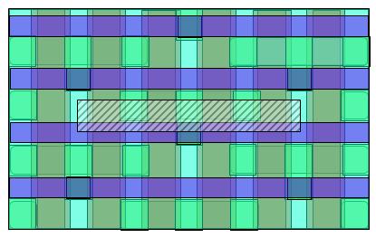
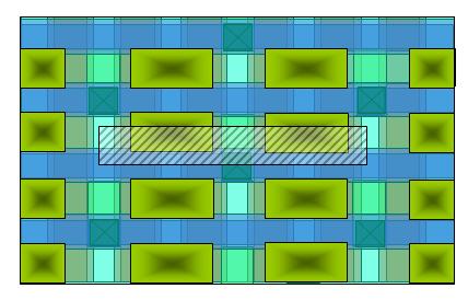
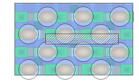
12 DRAM Fabrication Passivation Nitride Passivation HDP oxide Metal-2 Passivation Nitride Passivation HDP oxide Metal-2 TiN Capping Via CVD oxide Barrier metal Metal-1 CVD oxide Metal-1 ILD3 ILD3 ONO W-plug SN Stopper Nitride Plate poly SN DRAM Structure ILD2-B ILD2-A BL HM Nit. ILD1-B ILD1-A STI FOX SPP1 LPP SPP2 BLC1 GATE Cell Pad BL STI FOX BLC2 Cell Peri


13 Folded Structure Active A A A A BPSG:Borophosphosilicate glass ILD: interlayer dielectric BC: Bit line contact


14 (using CMP) CMP: chemical mechanical polishing LPP can be seen only in BC1 etch area. The area of cross-section view

15 HM: hard mask


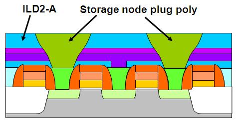
16 SN: storage node SPP: Storage node plug poly
 Plate poly formation ONO: oxide nitride oxide HSG: Hemispherical")
17 SN oxide removal using HF HSG poly Si formation Dielectric formation (ONO) Plate poly formation ONO: oxide nitride oxide HSG: Hemispherical grained
 (WL")

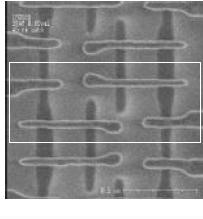
18 DRAM Cross-section Images (BL direction) (WL direction) M3 (Al) M2(Al) SN SN pad BL cell pad WL STI STI BL(W)
19 SGT DRAM Fabrication 113 A Capacitor cell A 108 (WL) A Open Structure (4F 2 ) Capacitor cell Select Transistor A A 101: BOX 102: N+ doped area 120: Nitride 108: Gate 107: Gate oxide 109: Landing plug poly 110: SN poly Si 111: ONO dielectric 112: plate poly 113: Bit line contact 115: Bit line plug poly


20 SGT DRAM Fabrication 101: BOX 102: N+ doped area 120: Nitride 108: Gate 107: Gate oxide

21 SGT DRAM Fabrication Tilted implantation 109: Landing plug poly


22 SGT DRAM Fabrication 110: SN poly Si 111: ONO dielectric 112: plate poly 113: Bit line metal 115: Bit line plug poly
 A Select Transistor 102 115 116 113 115")


23 SGT DRAM Fabrication 113 A A Capacitor cell Capacitor cell 108 (WL) A Select Transistor Capacitor cell Select Transistor A A 101: BOX 102: N+ doped area 120: Nitride 108: Gate 107: Gate oxide 109: Landing plug poly 110: SN poly Si 111: ONO dielectric 112: plate poly 113: Bit line metal 115: Bit line plug poly
24 SRAM SRAM : Non-Memory (or Logic) occupies 65% of total semiconductor market Cache memory for non-memory (CPU & GPU) Automobile or display MPU Portable device memory (cell phone), CIS Processor Cache Memory SRAM Main memory DRAM Archive I Magnetic disk / Magnetic tape Archive II Optical disk 24

25 SRAM The key issue of 6T SRAM is how to distinguish btw read and write. We have one wordline, so it should be high for read and write. Therefore we need to use two bitlines to operate SRAM. N2, N4: Access TR, P1, P2: Pull up PMOS, load N1, N3: Pull down NMOS, driver
26 SRAM Operation Butterfly curve
27 SRAM Read Read A _ A BL = 1 BL A BL Hold BL Turn off word Line Time (ps)

28 SRAM Write

29 SRAM Design (SNM)


30 SGT SRAM (reference) 81: BOX 82 & 114: Si 113: nitride mask 128: Si pillar 118: n+ doping 119: nitride spacer 120: salicide (self aligned silicide) 128: Si pillar 130& 134 & 136 : dielectric 131: gate dielectric 132: gate
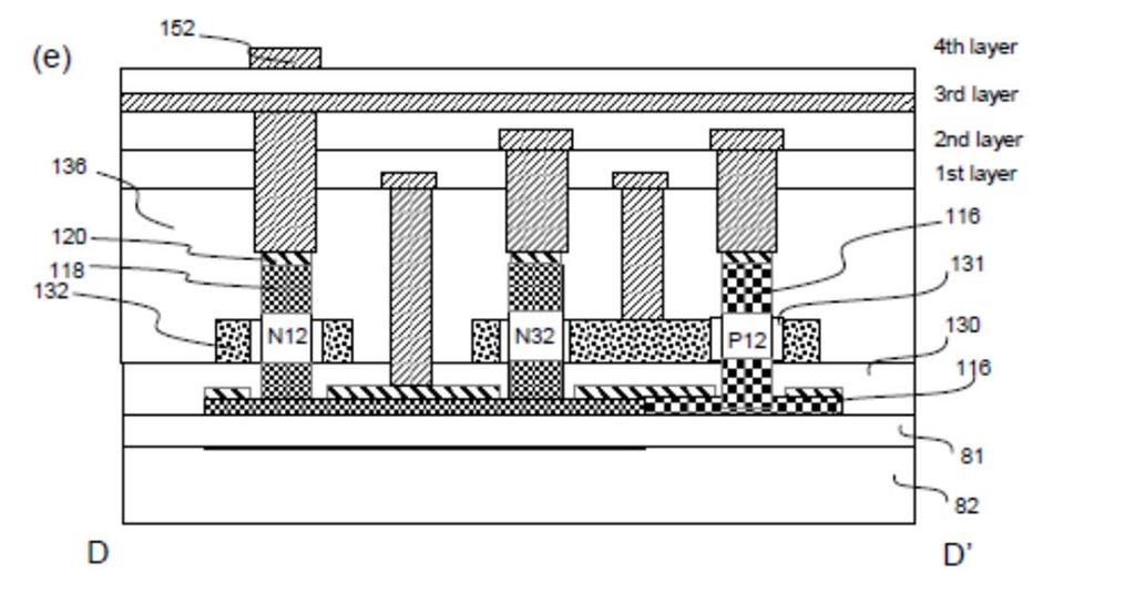
31 SGT SRAM (reference)
32 Announcement 1. Quiz will be held on 11 Oct from 1:00 to 2:00 2. HW #4 (due date: 6 Nov) Run at least two simulation sets (one SGT and one Trigate) that are designed during practice class. Draw transfer curves (Vd=0.1 & 1V) of the above simulations using log files. Obtain Vth, DIBL & SS from transfer curves. 3. HW #5 (due date: 13 Nov) Read Perspective of Giga DRAM and summarize in one A-4 page each. 32
Thin Film Transistors (TFT)
") Thin Film Transistors (TFT) a-si TFT - α-si:h (Hydrogenated amorphous Si) deposited with a PECVD system (low temp. process) replaces the single crystal Si substrate. - Inverted staggered structure with
Thin Film Transistors (TFT) a-si TFT - α-si:h (Hydrogenated amorphous Si) deposited with a PECVD system (low temp. process) replaces the single crystal Si substrate. - Inverted staggered structure with
Digital Integrated Circuits A Design Perspective. Semiconductor. Memories. Memories
 Digital Integrated Circuits A Design Perspective Semiconductor Chapter Overview Memory Classification Memory Architectures The Memory Core Periphery Reliability Case Studies Semiconductor Memory Classification
Semiconductor Memories
 Semiconductor References: Adapted from: Digital Integrated Circuits: A Design Perspective, J. Rabaey UCB Principles of CMOS VLSI Design: A Systems Perspective, 2nd Ed., N. H. E. Weste and K. Eshraghian
GMU, ECE 680 Physical VLSI Design 1
 ECE680: Physical VLSI Design Chapter VIII Semiconductor Memory (chapter 12 in textbook) 1 Chapter Overview Memory Classification Memory Architectures The Memory Core Periphery Reliability Case Studies
Digital Integrated Circuits A Design Perspective
 Semiconductor Memories Adapted from Chapter 12 of Digital Integrated Circuits A Design Perspective Jan M. Rabaey et al. Copyright 2003 Prentice Hall/Pearson Outline Memory Classification Memory Architectures
ESE 570: Digital Integrated Circuits and VLSI Fundamentals
 ESE 570: Digital Integrated Circuits and VLSI Fundamentals Lec 19: March 29, 2018 Memory Overview, Memory Core Cells Today! Charge Leakage/Charge Sharing " Domino Logic Design Considerations! Logic Comparisons!
Semiconductor memories
 Semiconductor memories Semiconductor Memories Data in Write Memory cell Read Data out Some design issues : How many cells? Function? Power consuption? Access type? How fast are read/write operations? Semiconductor
Lecture 25. Semiconductor Memories. Issues in Memory
 Lecture 25 Semiconductor Memories Issues in Memory Memory Classification Memory Architectures TheMemoryCore Periphery 1 Semiconductor Memory Classification RWM NVRWM ROM Random Access Non-Random Access
! Charge Leakage/Charge Sharing. " Domino Logic Design Considerations. ! Logic Comparisons. ! Memory. " Classification. " ROM Memories.
 ESE 57: Digital Integrated Circuits and VLSI Fundamentals Lec 9: March 9, 8 Memory Overview, Memory Core Cells Today! Charge Leakage/ " Domino Logic Design Considerations! Logic Comparisons! Memory " Classification
CMOS Inverter. Performance Scaling
 Announcements Exam #2 regrade requests due today. Homework #8 due today. Final Exam: Th June 12, 8:30 10:20am, CMU 120 (extension to 11:20am requested). Grades available for viewing via Catalyst. CMOS
ESE 570: Digital Integrated Circuits and VLSI Fundamentals
 ESE 570: Digital Integrated Circuits and VLSI Fundamentals Lec 21: April 4, 2017 Memory Overview, Memory Core Cells Penn ESE 570 Spring 2017 Khanna Today! Memory " Classification " ROM Memories " RAM Memory
Hw 6 and 7 Graded and available Project Phase 2 Graded Project Phase 3 Launch Today
 EECS141 1 Hw 8 Posted Last one to be graded Due Friday April 30 Hw 6 and 7 Graded and available Project Phase 2 Graded Project Phase 3 Launch Today EECS141 2 1 6 5 4 3 2 1 0 1.5 2 2.5 3 3.5 4 Frequency
PROGRESS AND ISSUES IN DIELECTRIC MATERIALS FOR SUB-100NM DRAM TECHNOLOGY ABSTRACT
 PROGRESS AND ISSUES IN DIELECTRIC MATERIALS FOR SUB-100NM DRAM TECHNOLOGY Kanta Saino Device Integration Group, Technology & Development Office, Elpida Memory Inc. 7-10 Yoshikawakogyodanchi, Higashihiroshima,
SEMICONDUCTOR MEMORIES
 SEMICONDUCTOR MEMORIES Semiconductor Memory Classification RWM NVRWM ROM Random Access Non-Random Access EPROM E 2 PROM Mask-Programmed Programmable (PROM) SRAM FIFO FLASH DRAM LIFO Shift Register CAM
CMOS Digital Integrated Circuits Lec 13 Semiconductor Memories
 Lec 13 Semiconductor Memories 1 Semiconductor Memory Types Semiconductor Memories Read/Write (R/W) Memory or Random Access Memory (RAM) Read-Only Memory (ROM) Dynamic RAM (DRAM) Static RAM (SRAM) 1. Mask
Semiconductor Memories
 !"#"$%&'()$*#+%$*,' -"+./"$0 1'!*0"#)'2*+03*.$"4* Jan M. Rabaey Anantha Chandrakasan Borivoje Nikolic Semiconductor Memories December 20, 2002 !"#$%&'()*&'*+&, Memory Classification Memory Architectures
Magnetic core memory (1951) cm 2 ( bit)
 cm 2 ( bit)") Magnetic core memory (1951) 16 16 cm 2 (128 128 bit) Semiconductor Memory Classification Read-Write Memory Non-Volatile Read-Write Memory Read-Only Memory Random Access Non-Random Access EPROM E 2 PROM
Magnetic core memory (1951) 16 16 cm 2 (128 128 bit) Semiconductor Memory Classification Read-Write Memory Non-Volatile Read-Write Memory Read-Only Memory Random Access Non-Random Access EPROM E 2 PROM
Chapter 3 Basics Semiconductor Devices and Processing
 Chapter 3 Basics Semiconductor Devices and Processing Hong Xiao, Ph. D. www2.austin.cc.tx.us/hongxiao/book.htm Hong Xiao, Ph. D. www2.austin.cc.tx.us/hongxiao/book.htm 1 Objectives Identify at least two
Semiconductor Memory Classification
 Semiconductor Memory Classification Read-Write Memory Non-Volatile Read-Write Memory Read-Only Memory Random Access Non-Random Access EPROM E 2 PROM Mask-Programmed Programmable (PROM) SRAM FIFO FLASH
Memory Trend. Memory Architectures The Memory Core Periphery
 Semiconductor Memories: an Introduction ti Talk Overview Memory Trend Memory Classification Memory Architectures The Memory Core Periphery Reliability Semiconductor Memory Trends (up to the 90 s) Memory
EE141-Fall 2011 Digital Integrated Circuits
 EE4-Fall 20 Digital Integrated Circuits Lecture 5 Memory decoders Administrative Stuff Homework #6 due today Project posted Phase due next Friday Project done in pairs 2 Last Lecture Last lecture Logical
Semiconductor Memories
 Digital Integrated Circuits A Design Perspective Jan M. Rabaey Anantha Chandrakasan Borivoje Nikolic Semiconductor Memories December 20, 2002 Chapter Overview Memory Classification Memory Architectures
Topics. Dynamic CMOS Sequential Design Memory and Control. John A. Chandy Dept. of Electrical and Computer Engineering University of Connecticut
 Topics Dynamic CMOS Sequential Design Memory and Control Dynamic CMOS In static circuits at every point in time (except when switching) the output is connected to either GND or V DD via a low resistance
EE241 - Spring 2000 Advanced Digital Integrated Circuits. References
 EE241 - Spring 2000 Advanced Digital Integrated Circuits Lecture 26 Memory References Rabaey, Digital Integrated Circuits Memory Design and Evolution, VLSI Circuits Short Course, 1998.» Gillingham, Evolution
EE141- Fall 2002 Lecture 27. Memory EE141. Announcements. We finished all the labs No homework this week Projects are due next Tuesday 9am EE141
 - Fall 2002 Lecture 27 Memory Announcements We finished all the labs No homework this week Projects are due next Tuesday 9am 1 Today s Lecture Memory:» SRAM» DRAM» Flash Memory 2 Floating-gate transistor
Lecture 34: Portable Systems Technology Background Professor Randy H. Katz Computer Science 252 Fall 1995
 Lecture 34: Portable Systems Technology Background Professor Randy H. Katz Computer Science 252 Fall 1995 RHK.F95 1 Technology Trends: Microprocessor Capacity 100000000 10000000 Pentium Transistors 1000000
Name: Answers. Mean: 83, Standard Deviation: 12 Q1 Q2 Q3 Q4 Q5 Q6 Total. ESE370 Fall 2015
 University of Pennsylvania Department of Electrical and System Engineering Circuit-Level Modeling, Design, and Optimization for Digital Systems ESE370, Fall 2015 Final Tuesday, December 15 Problem weightings
Chapter 7. Sequential Circuits Registers, Counters, RAM
 Chapter 7. Sequential Circuits Registers, Counters, RAM Register - a group of binary storage elements suitable for holding binary info A group of FFs constitutes a register Commonly used as temporary storage
Semiconductor Memories
 Digital Integrated Circuits A Design Perspective Jan M. Rabaey Anantha Chandrakasan Borivoje Nikolic Semiconductor Memories December 20, 2002 Chapter Overview Memory Classification Memory Architectures
Chapter Overview. Memory Classification. Memory Architectures. The Memory Core. Periphery. Reliability. Memory
 SRAM Design Chapter Overview Classification Architectures The Core Periphery Reliability Semiconductor Classification RWM NVRWM ROM Random Access Non-Random Access EPROM E 2 PROM Mask-Programmed Programmable
Lecture 3: CMOS Transistor Theory
 Lecture 3: CMOS Transistor Theory Outline Introduction MOS Capacitor nmos I-V Characteristics pmos I-V Characteristics Gate and Diffusion Capacitance 2 Introduction So far, we have treated transistors
CS 152 Computer Architecture and Engineering
 CS 152 Computer Architecture and Engineering Lecture 12 VLSI II 2005-2-24 John Lazzaro (www.cs.berkeley.edu/~lazzaro) TAs: Ted Hong and David Marquardt www-inst.eecs.berkeley.edu/~cs152/ Last Time: Device
! Memory. " RAM Memory. ! Cell size accounts for most of memory array size. ! 6T SRAM Cell. " Used in most commercial chips
 ESE 57: Digital Integrated Circuits and VLSI Fundamentals Lec : April 3, 8 Memory: Core Cells Today! Memory " RAM Memory " Architecture " Memory core " SRAM " DRAM " Periphery Penn ESE 57 Spring 8 - Khanna
Perspectives on giga-bit scaled DRAM technology generation
 Microelectronics Reliability 40 (2000) 191±206 Introductory invited paper Perspectives on giga-bit scaled DRAM technology generation Kinam Kim Technology Development, Memory Device Business, Samsung Electronics
Semiconductor Memories. Jan M. Rabaey Anantha Chandrakasan Borivoje Nikolic Paolo Spirito
 Semiconductor Memories Jan M. Rabaey Anantha Chandrakasan Borivoje Nikolic Paolo Spirito Memory Classification Memory Classification Read-Write Memory Non-Volatile Read-Write Memory Read-Only Memory Random
Moores Law for DRAM. 2x increase in capacity every 18 months 2006: 4GB
 MEMORY Moores Law for DRAM 2x increase in capacity every 18 months 2006: 4GB Corollary to Moores Law Cost / chip ~ constant (packaging) Cost / bit = 2X reduction / 18 months Current (2008) ~ 1 micro-cent
WARM SRAM: A Novel Scheme to Reduce Static Leakage Energy in SRAM Arrays
 WARM SRAM: A Novel Scheme to Reduce Static Leakage Energy in SRAM Arrays Mahadevan Gomathisankaran Iowa State University gmdev@iastate.edu Akhilesh Tyagi Iowa State University tyagi@iastate.edu ➀ Introduction
Multiple Gate CMOS and Beyond
 Multiple CMOS and Beyond Dept. of EECS, KAIST Yang-Kyu Choi Outline 1. Ultimate Scaling of MOSFETs - 3nm Nanowire FET - 8nm Non-Volatile Memory Device 2. Multiple Functions of MOSFETs 3. Summary 2 CMOS
ECE520 VLSI Design. Lecture 23: SRAM & DRAM Memories. Payman Zarkesh-Ha
 ECE520 VLSI Design Lecture 23: SRAM & DRAM Memories Payman Zarkesh-Ha Office: ECE Bldg. 230B Office hours: Wednesday 2:00-3:00PM or by appointment E-mail: pzarkesh@unm.edu Slide: 1 Review of Last Lecture
Administrative Stuff
 EE141- Spring 2004 Digital Integrated Circuits Lecture 30 PERSPECTIVES 1 Administrative Stuff Homework 10 posted just for practice. No need to turn in (hw 9 due today). Normal office hours next week. HKN
ESE570 Spring University of Pennsylvania Department of Electrical and System Engineering Digital Integrated Cicruits AND VLSI Fundamentals
 University of Pennsylvania Department of Electrical and System Engineering Digital Integrated Cicruits AND VLSI Fundamentals ESE570, Spring 2016 Final Friday, May 6 5 Problems with point weightings shown.
MOSFET: Introduction
 E&CE 437 Integrated VLSI Systems MOS Transistor 1 of 30 MOSFET: Introduction Metal oxide semiconductor field effect transistor (MOSFET) or MOS is widely used for implementing digital designs Its major
EE115C Winter 2017 Digital Electronic Circuits. Lecture 3: MOS RC Model, CMOS Manufacturing
 EE115C Winter 2017 Digital Electronic Circuits Lecture 3: MOS RC Model, CMOS Manufacturing Agenda MOS Transistor: RC Model (pp. 104-113) S R on D CMOS Manufacturing Process (pp. 36-46) S S C GS G G C GD
AE74 VLSI DESIGN JUN 2015
 Q.2 a. Write down the different levels of integration of IC industry. (4) b. With neat sketch explain briefly PMOS & NMOS enhancement mode transistor. N-MOS enhancement mode transistor:- This transistor
MOS Transistor Theory
 CHAPTER 3 MOS Transistor Theory Outline 2 1. Introduction 2. Ideal I-V Characteristics 3. Nonideal I-V Effects 4. C-V Characteristics 5. DC Transfer Characteristics 6. Switch-level RC Delay Models MOS
FERROELECTRIC RAM [FRAM] Submitted in partial fulfillment of the requirement for the award of degree of Bachelor of Technology in Computer Science
![FERROELECTRIC RAM [FRAM] Submitted in partial fulfillment of the requirement for the award of degree of Bachelor of Technology in Computer Science](/thumbs/72/67470194.jpg "FERROELECTRIC RAM [FRAM] Submitted in partial fulfillment of the requirement for the award of degree of Bachelor of Technology in Computer Science") A Seminar report On FERROELECTRIC RAM [FRAM] Submitted in partial fulfillment of the requirement for the award of degree of Bachelor of Technology in Computer Science SUBMITTED TO: www.studymafia.org SUBMITTED
A Seminar report On FERROELECTRIC RAM [FRAM] Submitted in partial fulfillment of the requirement for the award of degree of Bachelor of Technology in Computer Science SUBMITTED TO: www.studymafia.org SUBMITTED
University of Toronto. Final Exam
 University of Toronto Final Exam Date - Apr 18, 011 Duration:.5 hrs ECE334 Digital Electronics Lecturer - D. Johns ANSWER QUESTIONS ON THESE SHEETS USING BACKS IF NECESSARY 1. Equation sheet is on last
ESE570 Spring University of Pennsylvania Department of Electrical and System Engineering Digital Integrated Cicruits AND VLSI Fundamentals
 University of Pennsylvania Department of Electrical and System Engineering Digital Integrated Cicruits AND VLSI Fundamentals ESE570, Spring 017 Final Wednesday, May 3 4 Problems with point weightings shown.
ELEN0037 Microelectronic IC Design. Prof. Dr. Michael Kraft
 ELEN0037 Microelectronic IC Design Prof. Dr. Michael Kraft Lecture 2: Technological Aspects Technology Passive components Active components CMOS Process Basic Layout Scaling CMOS Technology Integrated
EE141. EE141-Spring 2006 Digital Integrated Circuits. Administrative Stuff. Class Material. Flash Memory. Read-Only Memory Cells MOS OR ROM
 EE141-pring 2006 igital Integrated Circuits Lecture 29 Flash memory Administrative tuff reat job on projects and posters! Homework #10 due today Lab reports due this week Friday lab in 353 Final exam May
Nanoscale CMOS Design Issues
 Nanoscale CMOS Design Issues Jaydeep P. Kulkarni Assistant Professor, ECE Department The University of Texas at Austin jaydeep@austin.utexas.edu Fall, 2017, VLSI-1 Class Transistor I-V Review Agenda Non-ideal
CARNEGIE MELLON UNIVERSITY DEPARTMENT OF ELECTRICAL AND COMPUTER ENGINEERING DIGITAL INTEGRATED CIRCUITS FALL 2002
 CARNEGIE MELLON UNIVERSITY DEPARTMENT OF ELECTRICAL AND COMPUTER ENGINEERING 18-322 DIGITAL INTEGRATED CIRCUITS FALL 2002 Final Examination, Monday Dec. 16, 2002 NAME: SECTION: Time: 180 minutes Closed
Tri-Gate Fully-Depleted CMOS Transistors: Fabrication, Design and Layout
 Tri-Gate Fully-Depleted CMOS Transistors: Fabrication, Design and Layout B.Doyle, J.Kavalieros, T. Linton, R.Rios B.Boyanov, S.Datta, M. Doczy, S.Hareland, B. Jin, R.Chau Logic Technology Development Intel
and V DS V GS V T (the saturation region) I DS = k 2 (V GS V T )2 (1+ V DS )
 I DS = k 2 (V GS V T )2 (1+ V DS )") ECE 4420 Spring 2005 Page 1 FINAL EXAMINATION NAME SCORE /100 Problem 1O 2 3 4 5 6 7 Sum Points INSTRUCTIONS: This exam is closed book. You are permitted four sheets of notes (three of which are your sheets
ECE 4420 Spring 2005 Page 1 FINAL EXAMINATION NAME SCORE /100 Problem 1O 2 3 4 5 6 7 Sum Points INSTRUCTIONS: This exam is closed book. You are permitted four sheets of notes (three of which are your sheets
JFET/MESFET. JFET: small gate current (reverse leakage of the gate-to-channel junction) More gate leakage than MOSFET, less than bipolar.
 More gate leakage than MOSFET, less than bipolar.") JFET/MESFET JFET: small gate current (reverse leakage of the gate-to-channel junction) More gate leakage than MOSFET, less than bipolar. JFET has higher transconductance than the MOSFET. Used in low-noise,
JFET/MESFET JFET: small gate current (reverse leakage of the gate-to-channel junction) More gate leakage than MOSFET, less than bipolar. JFET has higher transconductance than the MOSFET. Used in low-noise,
CS 152 Computer Architecture and Engineering. Lecture 11 VLSI
 CS 152 Computer Architecture and Engineering Lecture 11 VLSI 2005-10-6 John Lazzaro (www.cs.berkeley.edu/~lazzaro) TAs: David Marquardt and Udam Saini www-inst.eecs.berkeley.edu/~cs152/ Today: State Storage
EECS 141: FALL 05 MIDTERM 1
 University of California College of Engineering Department of Electrical Engineering and Computer Sciences D. Markovic TuTh 11-1:3 Thursday, October 6, 6:3-8:pm EECS 141: FALL 5 MIDTERM 1 NAME Last SOLUTION
Power Dissipation. Where Does Power Go in CMOS?
 Power Dissipation [Adapted from Chapter 5 of Digital Integrated Circuits, 2003, J. Rabaey et al.] Where Does Power Go in CMOS? Dynamic Power Consumption Charging and Discharging Capacitors Short Circuit
VLSI GATE LEVEL DESIGN UNIT - III P.VIDYA SAGAR ( ASSOCIATE PROFESSOR) Department of Electronics and Communication Engineering, VBIT
 Department of Electronics and Communication Engineering, VBIT") VLSI UNIT - III GATE LEVEL DESIGN P.VIDYA SAGAR ( ASSOCIATE PROFESSOR) contents GATE LEVEL DESIGN : Logic Gates and Other complex gates, Switch logic, Alternate gate circuits, Time Delays, Driving large
VLSI UNIT - III GATE LEVEL DESIGN P.VIDYA SAGAR ( ASSOCIATE PROFESSOR) contents GATE LEVEL DESIGN : Logic Gates and Other complex gates, Switch logic, Alternate gate circuits, Time Delays, Driving large
ECE251. VLSI System Design
 ECE251. VLSI System Design Project 4 SRAM Cell and Memory Array Operation Area Memory core 4661 mm 2 (256bit) Row Decoder 204.7 mm 2 Collumn Decoder Overall Design Predecoder 156.1 mm 2 Mux 629.2 mm 2
Digital Integrated Circuits A Design Perspective
 igital Integrated Circuits esign Perspective esigning Combinational Logic Circuits 1 Combinational vs. Sequential Logic In Combinational Logic Circuit Out In Combinational Logic Circuit Out State Combinational
ESE570 Spring University of Pennsylvania Department of Electrical and System Engineering Digital Integrated Cicruits AND VLSI Fundamentals
 University of Pennsylvania Department of Electrical and System Engineering Digital Integrated Cicruits AND VLSI Fundamentals ESE570, Spring 2018 Final Monday, Apr 0 5 Problems with point weightings shown.
EE382M-14 CMOS Analog Integrated Circuit Design
 EE382M-14 CMOS Analog Integrated Circuit Design Lecture 3, MOS Capacitances, Passive Components, and Layout of Analog Integrated Circuits MOS Capacitances Type of MOS transistor capacitors Depletion capacitance
Floating Point Representation and Digital Logic. Lecture 11 CS301
 Floating Point Representation and Digital Logic Lecture 11 CS301 Administrative Daily Review of today s lecture w Due tomorrow (10/4) at 8am Lab #3 due Friday (9/7) 1:29pm HW #5 assigned w Due Monday 10/8
Memory, Latches, & Registers
 Memory, Latches, & Registers 1) Structured Logic Arrays 2) Memory Arrays 3) Transparent Latches 4) How to save a few bucks at toll booths 5) Edge-triggered Registers L13 Memory 1 General Table Lookup Synthesis
S No. Questions Bloom s Taxonomy Level UNIT-I
 GROUP-A (SHORT ANSWER QUESTIONS) S No. Questions Bloom s UNIT-I 1 Define oxidation & Classify different types of oxidation Remember 1 2 Explain about Ion implantation Understand 1 3 Describe lithography
EE410 vs. Advanced CMOS Structures
 EE410 vs. Advanced CMOS Structures Prof. Krishna S Department of Electrical Engineering S 1 EE410 CMOS Structure P + poly-si N + poly-si Al/Si alloy LPCVD PSG P + P + N + N + PMOS N-substrate NMOS P-well
Introduction to CMOS VLSI Design Lecture 1: Introduction
 Introduction to CMOS VLSI Design Lecture 1: Introduction David Harris, Harvey Mudd College Kartik Mohanram and Steven Levitan University of Pittsburgh Introduction Integrated circuits: many transistors
Lecture 0: Introduction
 Lecture 0: Introduction Introduction q Integrated circuits: many transistors on one chip q Very Large Scale Integration (VLSI): bucketloads! q Complementary Metal Oxide Semiconductor Fast, cheap, low power
Analysis and design of a new SRAM memory cell based on vertical lambda bipolar transistor
 Microelectronics Journal 34 (003) 855 863 www.elsevier.com/locate/mejo Analysis and design of a new SRAM memory cell based on vertical lambda bipolar transistor Shang-Ming Wang*, Ching-Yuan Wu Institute
FIB Voltage Contrast for Failure Localisation on CMOS Circuits an Overview
 for Failure Localisation on CMOS Circuits an Overview 8th European FIB User Group Meeting Zürich 2004 Dr. rer. nat. Rüdiger Rosenkranz Infineon Technologies Dresden Physical Failure Analysis Page 1 Never
Circuits. L5: Fabrication and Layout -2 ( ) B. Mazhari Dept. of EE, IIT Kanpur. B. Mazhari, IITK. G-Number
 B. Mazhari Dept. of EE, IIT Kanpur. B. Mazhari, IITK. G-Number") EE610: CMOS Analog Circuits L5: Fabrication and Layout -2 (12.8.2013) B. Mazhari Dept. of EE, IIT Kanpur 44 Passive Components: Resistor Besides MOS transistors, sometimes one requires to implement passive
EE610: CMOS Analog Circuits L5: Fabrication and Layout -2 (12.8.2013) B. Mazhari Dept. of EE, IIT Kanpur 44 Passive Components: Resistor Besides MOS transistors, sometimes one requires to implement passive
2. (2pts) What is the major difference between an epitaxial layer and a polysilicon layer?
 What is the major difference between an epitaxial layer and a polysilicon layer?") EE 330 Exam 1 Spring 2017 Name Instructions: Students may bring 1 page of notes (front and back) to this exam and a calculator but the use of any device that has wireless communication capability is prohibited.
EE 330 Exam 1 Spring 2017 Name Instructions: Students may bring 1 page of notes (front and back) to this exam and a calculator but the use of any device that has wireless communication capability is prohibited.
C.K. Ken Yang UCLA Courtesy of MAH EE 215B
 Decoders: Logical Effort Applied C.K. Ken Yang UCLA yang@ee.ucla.edu Courtesy of MAH 1 Overview Reading Rabaey 6.2.2 (Ratio-ed logic) W&H 6.2.2 Overview We have now gone through the basics of decoders,
Self-study problems and questions Processing and Device Technology, FFF110/FYSD13
 Self-study problems and questions Processing and Device Technology, FFF110/FYSD13 Version 2016_01 In addition to the problems discussed at the seminars and at the lectures, you can use this set of problems
CMOS Devices. PN junctions and diodes NMOS and PMOS transistors Resistors Capacitors Inductors Bipolar transistors
 CMOS Devices PN junctions and diodes NMOS and PMOS transistors Resistors Capacitors Inductors Bipolar transistors PN Junctions Diffusion causes depletion region D.R. is insulator and establishes barrier
ESE 570: Digital Integrated Circuits and VLSI Fundamentals
 ESE 570: Digital Integrated Circuits and VLSI Fundamentals Lec 18: March 27, 2018 Dynamic Logic, Charge Injection Lecture Outline! Sequential MOS Logic " D-Latch " Timing Constraints! Dynamic Logic " Domino
HN58C256 Series word 8-bit Electrically Erasable and Programmable CMOS ROM
 32768-word 8-bit Electrically Erasable and Programmable CMOS ROM ADE-203-092G (Z) Rev. 7.0 Nov. 29, 1994 Description The Hitachi HN58C256 is a electrically erasable and programmable ROM organized as 32768-word
P. R. Nelson 1 ECE418 - VLSI. Midterm Exam. Solutions
 P. R. Nelson 1 ECE418 - VLSI Midterm Exam Solutions 1. (8 points) Draw the cross-section view for A-A. The cross-section view is as shown below.. ( points) Can you tell which of the metal1 regions is the
LH5P8128. CMOS 1M (128K 8) Pseudo-Static RAM PIN CONNECTIONS
 Pseudo-Static RAM PIN CONNECTIONS") LH5P8128 FEATURES 131,072 8 bit organization Access times (MAX.): 60/80/100 ns Cycle times (MIN.): 100/130/160 ns Single +5 V power supply Power consumption: Operating: 572/385/275 mw (MAX.) Standby (CMOS
LH5P8128 FEATURES 131,072 8 bit organization Access times (MAX.): 60/80/100 ns Cycle times (MIN.): 100/130/160 ns Single +5 V power supply Power consumption: Operating: 572/385/275 mw (MAX.) Standby (CMOS
ECE-470 Digital Design II Memory Test. Memory Cells Per Chip. Failure Mechanisms. Motivation. Test Time in Seconds (Memory Size: n Bits) Fault Types
 Fault Types") ECE-470 Digital Design II Memory Test Motivation Semiconductor memories are about 35% of the entire semiconductor market Memories are the most numerous IPs used in SOC designs Number of bits per chip continues
ECE-470 Digital Design II Memory Test Motivation Semiconductor memories are about 35% of the entire semiconductor market Memories are the most numerous IPs used in SOC designs Number of bits per chip continues
VLSI. Faculty. Srikanth
 J.B. Institute of Engineering & Technology Department of CSE COURSE FILE VLSI Faculty Srikanth J.B. Institute of Engineering & Technology Department of CSE SYLLABUS Subject Name: VLSI Subject Code: VLSI
CVD: General considerations.
 CVD: General considerations. PVD: Move material from bulk to thin film form. Limited primarily to metals or simple materials. Limited by thermal stability/vapor pressure considerations. Typically requires
Semiconductor Integrated Process Design (MS 635)
") Semiconductor Integrated Process Design (MS 635) Instructor: Prof. Keon Jae Lee - Office: 응용공학동 #4306, Tel: #3343 - Email: keonlee@kaist.ac.kr Lecture: (Tu, Th), 1:00-2:15 #2425 Office hour: Tues & Thur
Semiconductor Integrated Process Design (MS 635) Instructor: Prof. Keon Jae Lee - Office: 응용공학동 #4306, Tel: #3343 - Email: keonlee@kaist.ac.kr Lecture: (Tu, Th), 1:00-2:15 #2425 Office hour: Tues & Thur
LH5P832. CMOS 256K (32K 8) Pseudo-Static RAM
 Pseudo-Static RAM") LH5P832 CMOS 256K (32K 8) Pseudo-Static RAM FEATURES 32,768 8 bit organization Access time: 100/120 ns (MAX.) Cycle time: 160/190 ns (MIN.) Power consumption: Operating: 357.5/303 mw Standby: 16.5 mw TTL
LH5P832 CMOS 256K (32K 8) Pseudo-Static RAM FEATURES 32,768 8 bit organization Access time: 100/120 ns (MAX.) Cycle time: 160/190 ns (MIN.) Power consumption: Operating: 357.5/303 mw Standby: 16.5 mw TTL
Impact of parametric mismatch and fluctuations on performance and yield of deep-submicron CMOS technologies. Philips Research, The Netherlands
 Impact of parametric mismatch and fluctuations on performance and yield of deep-submicron CMOS technologies Hans Tuinhout, The Netherlands motivation: from deep submicron digital ULSI parametric spread
L ECE 4211 UConn F. Jain Scaling Laws for NanoFETs Chapter 10 Logic Gate Scaling
 L13 04202017 ECE 4211 UConn F. Jain Scaling Laws for NanoFETs Chapter 10 Logic Gate Scaling Scaling laws: Generalized scaling (GS) p. 610 Design steps p.613 Nanotransistor issues (page 626) Degradation
MTJ-Based Nonvolatile Logic-in-Memory Architecture and Its Application
 2011 11th Non-Volatile Memory Technology Symposium @ Shanghai, China, Nov. 9, 20112 MTJ-Based Nonvolatile Logic-in-Memory Architecture and Its Application Takahiro Hanyu 1,3, S. Matsunaga 1, D. Suzuki
Introduction and Background
 Analog CMOS Integrated Circuit Design Introduction and Background Dr. Jawdat Abu-Taha Department of Electrical and Computer Engineering Islamic University of Gaza jtaha@iugaza.edu.ps 1 Marking Assignments
DRAMATIC advances in technology scaling have given us
 IEEE JOURNAL OF SOLID-STATE CIRCUITS, VOL. 39, NO. 6, JUNE 2004 919 Complementary Ferroelectric-Capacitor Logic for Low-Power Logic-in-Memory VLSI Hiromitsu Kimura, Member, IEEE, Takahiro Hanyu, Member,
Chapter 2 CMOS Transistor Theory. Jin-Fu Li Department of Electrical Engineering National Central University Jungli, Taiwan
 Chapter 2 CMOS Transistor Theory Jin-Fu Li Department of Electrical Engineering National Central University Jungli, Taiwan Outline Introduction MOS Device Design Equation Pass Transistor Jin-Fu Li, EE,
Delay and Energy Consumption Analysis of Conventional SRAM
 World Academy of Science, Engineering and Technology 13 8 Delay and Energy Consumption Analysis of Conventional SAM Arash Azizi-Mazreah, Mohammad T. Manzuri Shalmani, Hamid Barati, and Ali Barati Abstract
F14 Memory Circuits. Lars Ohlsson
 Lars Ohlsson 2018-10-18 F14 Memory Circuits Outline Combinatorial vs. sequential logic circuits Analogue multivibrator circuits Noise in digital circuits CMOS latch CMOS SR flip flop 6T SRAM cell 1T DRAM
EEC 116 Lecture #5: CMOS Logic. Rajeevan Amirtharajah Bevan Baas University of California, Davis Jeff Parkhurst Intel Corporation
 EEC 116 Lecture #5: CMOS Logic Rajeevan mirtharajah Bevan Baas University of California, Davis Jeff Parkhurst Intel Corporation nnouncements Quiz 1 today! Lab 2 reports due this week Lab 3 this week HW
1. Chapter 1: Introduction
 1. Chapter 1: Introduction Non-volatile memories with ferroelectric capacitor materials are also known as ferroelectric random access memories (FRAMs). Present research focuses on integration of ferroelectric
Single Event Effects: SRAM
 Scuola Nazionale di Legnaro 29/3/2007 Single Event Effects: SRAM Alessandro Paccagnella Dipartimento di Ingegneria dell Informazione Università di Padova alessandro.paccagnella@unipd.it OUTLINE Introduction
And device degradation. Slide 1
 And device degradation Slide 1 Z. Guo, ISSSCC 2018 Inter-die Variation & Cell Failures Failures in SRAM Array Overall Cell Failure: [ ] P = P Fail = P A! R! W! H F F F F F P MEM Redundant Columns PASS
From Physics to Logic
 From Physics to Logic This course aims to introduce you to the layers of abstraction of modern computer systems. We won t spend much time below the level of bits, bytes, words, and functional units, but
(22) Filed: Feb. 22, 2000 Primary Examiner-Carl Whitehead, Jr. 30 F Application O O P tv Dat. ASSistant Examiner Toniae M. Thomas
 Filed: Feb. 22, 2000 Primary Examiner-Carl Whitehead, Jr. 30 F Application O O P tv Dat. ASSistant Examiner Toniae M. Thomas") (12) United States Patent Hwang et al. USOO6479343B1 (10) Patent No.: (45) Date of Patent: Nov. 12, 2002 (54) DRAM CELL CAPACITOR AND MANUFACTURING METHOD THEREOF (75) Inventors: Yoo-Sang Hwang, Suwon;
(12) United States Patent Hwang et al. USOO6479343B1 (10) Patent No.: (45) Date of Patent: Nov. 12, 2002 (54) DRAM CELL CAPACITOR AND MANUFACTURING METHOD THEREOF (75) Inventors: Yoo-Sang Hwang, Suwon;
Lecture 4: CMOS Transistor Theory
 Introduction to CMOS VLSI Design Lecture 4: CMOS Transistor Theory David Harris, Harvey Mudd College Kartik Mohanram and Steven Levitan University of Pittsburgh Outline q Introduction q MOS Capacitor q