Semiconductor Memories. Jan M. Rabaey Anantha Chandrakasan Borivoje Nikolic Paolo Spirito
|
|
|
- Natalie Nicholson
- 5 years ago
- Views:
Transcription
1 Semiconductor Memories Jan M. Rabaey Anantha Chandrakasan Borivoje Nikolic Paolo Spirito
2 Memory Classification
3 Memory Classification Read-Write Memory Non-Volatile Read-Write Memory Read-Only Memory Random Access Non-Random Access EPROM E 2 PROM Mask-Programmed Programmable (PROM) SRAM DRAM FIFO LIFO Shift Register CAM FLASH
4 Memory Classification
5 Memory access time

6 Memory timing: definitions
7
8 RAM memory Architecture M bits M bits S 0 S 1 Word 0 Word 1 Word 2 Storage cell A 0 A 1 S 0 Word 0 Word 1 Word 2 Storage cell Word N 2 A K 1 Word N 2 S N-1 Word N 1 Word N 1 K = log 2 N S N 1 Input-Output M bits Intuitive architecture for N x M memory Too many select signals: N words => N select signals Input-Output M bits Decoder reduces the number of select signals K = log 2 N
9 Matrix memory organization
10 Matrix memory organization A K A K+1 A K+2 A L 1 A A A A A 2 L K M = 2 K Amplify swing to rail-to-rail amplitude A 0.. A K 1 Selects appropriate word La word line abilita tutte le celle sulla riga consumo di potenza La bit line permette di leggere/scrivere la cella desiderata


11 Hierarchical memory architecture P 1 Advantages: 1. Shorter wires within blocks 2. Block address activates only 1 block => power savings
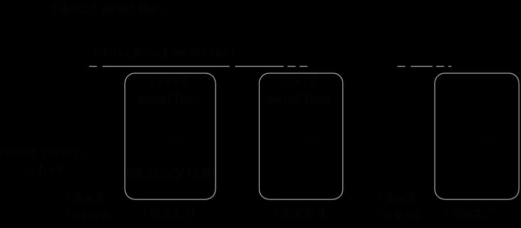
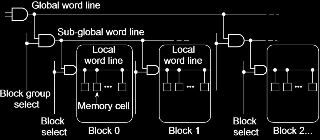
12 Hierarchical memory architecture
13 Memory array architecture

14 Power dissipation in memories
15
16 Memory organization
17 6-Transistor CMOS SRAM Cell
18 6-Transistor CMOS SRAM Cell WL V DD M 2 M 4 Q Q M 6 M 5 M 1 M 3 BL BL
19 SRAM Write operation: ex. Q = 1 WL V DD M 4 Q = 0 M 6 M 5 Q = 1 M 1 V DD BL = 1 BL = 0 IP: Q=1 WL=1 to activate M5 e M6 BL=0 M6 is ON Q goes to 0 since M4 turn OFF during the transient BL=1 M6 is ON Q goes to 0 since M1 turn OFF during the transient
20 SRAM Write operation

21 SRAM Read operation: ex. Q = 1 WL V DD BL M 4 Q = 0 Q = 1 M 6 M 5 BL V DD M 1 V DD V DD C bit C bit
22 Resistive-load SRAM cell WL V DD R L R L M 3 Q Q M 4 BL M 1 M 2 BL Static power dissipation: want R L large Bit lines precharged to V DD to address t p problem
23 SRAM Characteristic
24 Sense amplifiers small transition s.a. input output Il sense amplifier è un circuito in grado di amplificare le variazioni presenti sul segnale di ingresso un piccolo sbilanciamento delle tensioni su BL e BL viene amplificato.

25 Memory Classification 2 L K A K A K+1 A K+2 A L 1 A A A A A M = 2 K Amplify swing to rail-to-rail amplitude A 0.. A K 1 Selects appropriate word
26 Transposed-bit-line architecture BL C cross BL BL SA BL (a) Straightforward bit-line routing C cross BL k-1 BL k SA BL k BL k+1 (b) Transposed bit-line architecture
27

 C S C S + C BL")
28 1-Transistor DRAM Cell X Write: C S is charged or discharged by asserting WL and BL. Read: Charge redistribution takes places between bit line and storage capacitance ΔV = V BL V PRE = (V X V PRE ) C S C S + C BL Voltage swing is small; typically around 250 mv.

29 Read operation

30 Write operation Avrò in transitorio la cui durata dipende dalla resistività di M1


31 Advanced 1-T DRAM cell Word line Insulating Layer Cell plate Capacitor dielectric layer Cell Plate Si Refilling Poly Transfer gate Storage electrode Isolation Si Substrate 2nd Field Oxide Trench Cell Stacked-capacitor Cell

32 Future DRAM Technology
33 1-Transistor DRAM Cell 1T DRAM requires a sense amplifier for each bit line, due to charge redistribution read-out. DRAM memory cells are single ended in contrast to SRAM cells. The read-out of the 1T DRAM cell is destructive refresh is necessary for correct operation. The 1T cell requires presence of a capacitance that must be explicitly included in the design. When writing a 1 into a DRAM cell, a threshold voltage is lost (M1 in pass transistor configuration) this loss can be circumvented by boot-strapping the word lines to a value higher than VDD
34 Noise sources in 1-T DRAM C WBL BL substrate Adjacent BL WL leakage C S electrode C cross
35 Read-Write RAM
36 Perifery Decoders Sense Amplifiers Input/Output Buffers Control & Timing Circuitry
37 8-bit AND Decoder Collection of 2 M complex logic gates organized in regular and dense fashion WL 0 = A 7 A 6 A 5 A 4 A 3 A 2 A 1 A 0 WL 1 = A 7 A 6 A 5 A 4 A 3 A 2 A 1 A 0 WL 255 = A 7 A 6 A 5 A 4 A 3 A 2 A 1 A 0 1 NAND with 8 inputs and 1 NOT very big area and very slow 2 stages Decoder
38 10-bit NOR Decoder WL 0 = A 7 +A 6 +A 5 +A 4 +A 3 +A 2 +A 1 +A 0 WL 1 = A 7 +A 6 +A 5 +A 4 +A 3 +A 2 +A 1 +A 0 WL 255 = A 7 +A 6 +A 5 +A 4 +A 3 +A 2 +A 1 +A 0 1 NOR with 8 inputs (16 T) 1 stage Decoder Number T: 256 x 16 = 4096 T
39 Hierarchical decoders WL 0 = A 7 A 6 A 5 A 4 A 3 A 2 A 1 A 0 WL 0 = A 7 A 6 A 5 A 4 A 3 A 2 A 1 A 0 WL 0 = (A 7 +A 6 )(A 5 +A 4 )(A 3 +A 2 )(A 1 +A 0 ) The address is partitioned into sections of 2 bits that are decoded in advance. The resulting signal are then combined using 4-input NAND gates 1 4-input NAND 4 2-input NOR
40 Hierarchical decoders Multi-stage implementation improves performance WL 1 WL 0 A 0 A 1 A 0 A 1 A 0 A 1 A 0 A 1 A 2 A 3 A 2 A 3 A 2 A 3 A 2 A 3 NAND decoder using 2-input pre-decoders A 1 A 0 A 0 A 1 A 3 A 2 A 3 A 2 Number T: (256x8T)+(4 x 4 x 4T) = 2112 T 52% smaller & faster
41 Hierarchical decoders Multi-stage implementation improves performance WL 1 WL 0 A 0 A 1 A 0 A 1 A 0 A 1 A 0 A 1 A 2 A 3 A 2 A 3 A 2 A 3 A 2 A 3 NAND decoder using 2-input pre-decoders A 1 A 0 A 0 A 1 A 3 A 2 A 3 A 2 Number T: (256x8T)+(4 x 4 x 4T) = 2112 T 52% smaller & faster
42 Column decoder: pass-transistor based BL 0 BL 1 BL 2 BL 3 A 0 S 0 S 1 S 2 A 1 S 3 Advantages: speed (t pd does not add to overall memory access time) Only one extra transistor in signal path Disadvantage: Large transistor count D
43 4-to-1 Tree-based column decoder BL 0 BL 1 BL 2 BL 3 A 0 A 0 A 1 A 1 D Number of devices drastically reduced, but delay increases quadratically with # of sections and becomes prohibitive for large decoders. Solutions: i) buffers; ii) progressive sizing; iii) combination of tree and pass-transistor approaches
Digital Integrated Circuits A Design Perspective. Semiconductor. Memories. Memories
 Digital Integrated Circuits A Design Perspective Semiconductor Chapter Overview Memory Classification Memory Architectures The Memory Core Periphery Reliability Case Studies Semiconductor Memory Classification
Digital Integrated Circuits A Design Perspective
 Semiconductor Memories Adapted from Chapter 12 of Digital Integrated Circuits A Design Perspective Jan M. Rabaey et al. Copyright 2003 Prentice Hall/Pearson Outline Memory Classification Memory Architectures
Semiconductor Memories
 Semiconductor References: Adapted from: Digital Integrated Circuits: A Design Perspective, J. Rabaey UCB Principles of CMOS VLSI Design: A Systems Perspective, 2nd Ed., N. H. E. Weste and K. Eshraghian
SEMICONDUCTOR MEMORIES
 SEMICONDUCTOR MEMORIES Semiconductor Memory Classification RWM NVRWM ROM Random Access Non-Random Access EPROM E 2 PROM Mask-Programmed Programmable (PROM) SRAM FIFO FLASH DRAM LIFO Shift Register CAM
Semiconductor Memories
 !"#"$%&'()$*#+%$*,' -"+./"$0 1'!*0"#)'2*+03*.$"4* Jan M. Rabaey Anantha Chandrakasan Borivoje Nikolic Semiconductor Memories December 20, 2002 !"#$%&'()*&'*+&, Memory Classification Memory Architectures
Semiconductor memories
 Semiconductor memories Semiconductor Memories Data in Write Memory cell Read Data out Some design issues : How many cells? Function? Power consuption? Access type? How fast are read/write operations? Semiconductor
GMU, ECE 680 Physical VLSI Design 1
 ECE680: Physical VLSI Design Chapter VIII Semiconductor Memory (chapter 12 in textbook) 1 Chapter Overview Memory Classification Memory Architectures The Memory Core Periphery Reliability Case Studies
Lecture 25. Semiconductor Memories. Issues in Memory
 Lecture 25 Semiconductor Memories Issues in Memory Memory Classification Memory Architectures TheMemoryCore Periphery 1 Semiconductor Memory Classification RWM NVRWM ROM Random Access Non-Random Access
Magnetic core memory (1951) cm 2 ( bit)
 cm 2 ( bit)") Magnetic core memory (1951) 16 16 cm 2 (128 128 bit) Semiconductor Memory Classification Read-Write Memory Non-Volatile Read-Write Memory Read-Only Memory Random Access Non-Random Access EPROM E 2 PROM
Magnetic core memory (1951) 16 16 cm 2 (128 128 bit) Semiconductor Memory Classification Read-Write Memory Non-Volatile Read-Write Memory Read-Only Memory Random Access Non-Random Access EPROM E 2 PROM
Semiconductor Memory Classification
 Semiconductor Memory Classification Read-Write Memory Non-Volatile Read-Write Memory Read-Only Memory Random Access Non-Random Access EPROM E 2 PROM Mask-Programmed Programmable (PROM) SRAM FIFO FLASH
Chapter Overview. Memory Classification. Memory Architectures. The Memory Core. Periphery. Reliability. Memory
 SRAM Design Chapter Overview Classification Architectures The Core Periphery Reliability Semiconductor Classification RWM NVRWM ROM Random Access Non-Random Access EPROM E 2 PROM Mask-Programmed Programmable
EE241 - Spring 2000 Advanced Digital Integrated Circuits. References
 EE241 - Spring 2000 Advanced Digital Integrated Circuits Lecture 26 Memory References Rabaey, Digital Integrated Circuits Memory Design and Evolution, VLSI Circuits Short Course, 1998.» Gillingham, Evolution
Hw 6 and 7 Graded and available Project Phase 2 Graded Project Phase 3 Launch Today
 EECS141 1 Hw 8 Posted Last one to be graded Due Friday April 30 Hw 6 and 7 Graded and available Project Phase 2 Graded Project Phase 3 Launch Today EECS141 2 1 6 5 4 3 2 1 0 1.5 2 2.5 3 3.5 4 Frequency
Topics. Dynamic CMOS Sequential Design Memory and Control. John A. Chandy Dept. of Electrical and Computer Engineering University of Connecticut
 Topics Dynamic CMOS Sequential Design Memory and Control Dynamic CMOS In static circuits at every point in time (except when switching) the output is connected to either GND or V DD via a low resistance
ESE 570: Digital Integrated Circuits and VLSI Fundamentals
 ESE 570: Digital Integrated Circuits and VLSI Fundamentals Lec 21: April 4, 2017 Memory Overview, Memory Core Cells Penn ESE 570 Spring 2017 Khanna Today! Memory " Classification " ROM Memories " RAM Memory
EE141- Fall 2002 Lecture 27. Memory EE141. Announcements. We finished all the labs No homework this week Projects are due next Tuesday 9am EE141
 - Fall 2002 Lecture 27 Memory Announcements We finished all the labs No homework this week Projects are due next Tuesday 9am 1 Today s Lecture Memory:» SRAM» DRAM» Flash Memory 2 Floating-gate transistor
ESE 570: Digital Integrated Circuits and VLSI Fundamentals
 ESE 570: Digital Integrated Circuits and VLSI Fundamentals Lec 19: March 29, 2018 Memory Overview, Memory Core Cells Today! Charge Leakage/Charge Sharing " Domino Logic Design Considerations! Logic Comparisons!
! Charge Leakage/Charge Sharing. " Domino Logic Design Considerations. ! Logic Comparisons. ! Memory. " Classification. " ROM Memories.
 ESE 57: Digital Integrated Circuits and VLSI Fundamentals Lec 9: March 9, 8 Memory Overview, Memory Core Cells Today! Charge Leakage/ " Domino Logic Design Considerations! Logic Comparisons! Memory " Classification
Semiconductor Memories
 Digital Integrated Circuits A Design Perspective Jan M. Rabaey Anantha Chandrakasan Borivoje Nikolic Semiconductor Memories December 20, 2002 Chapter Overview Memory Classification Memory Architectures
Semiconductor Memories
 Digital Integrated Circuits A Design Perspective Jan M. Rabaey Anantha Chandrakasan Borivoje Nikolic Semiconductor Memories December 20, 2002 Chapter Overview Memory Classification Memory Architectures
Memory Trend. Memory Architectures The Memory Core Periphery
 Semiconductor Memories: an Introduction ti Talk Overview Memory Trend Memory Classification Memory Architectures The Memory Core Periphery Reliability Semiconductor Memory Trends (up to the 90 s) Memory
Administrative Stuff
 EE141- Spring 2004 Digital Integrated Circuits Lecture 30 PERSPECTIVES 1 Administrative Stuff Homework 10 posted just for practice. No need to turn in (hw 9 due today). Normal office hours next week. HKN
ECE520 VLSI Design. Lecture 23: SRAM & DRAM Memories. Payman Zarkesh-Ha
 ECE520 VLSI Design Lecture 23: SRAM & DRAM Memories Payman Zarkesh-Ha Office: ECE Bldg. 230B Office hours: Wednesday 2:00-3:00PM or by appointment E-mail: pzarkesh@unm.edu Slide: 1 Review of Last Lecture
! Memory. " RAM Memory. ! Cell size accounts for most of memory array size. ! 6T SRAM Cell. " Used in most commercial chips
 ESE 57: Digital Integrated Circuits and VLSI Fundamentals Lec : April 3, 8 Memory: Core Cells Today! Memory " RAM Memory " Architecture " Memory core " SRAM " DRAM " Periphery Penn ESE 57 Spring 8 - Khanna
EE141. EE141-Spring 2006 Digital Integrated Circuits. Administrative Stuff. Class Material. Flash Memory. Read-Only Memory Cells MOS OR ROM
 EE141-pring 2006 igital Integrated Circuits Lecture 29 Flash memory Administrative tuff reat job on projects and posters! Homework #10 due today Lab reports due this week Friday lab in 353 Final exam May
CMOS Digital Integrated Circuits Lec 13 Semiconductor Memories
 Lec 13 Semiconductor Memories 1 Semiconductor Memory Types Semiconductor Memories Read/Write (R/W) Memory or Random Access Memory (RAM) Read-Only Memory (ROM) Dynamic RAM (DRAM) Static RAM (SRAM) 1. Mask
EE141-Fall 2011 Digital Integrated Circuits
 EE4-Fall 20 Digital Integrated Circuits Lecture 5 Memory decoders Administrative Stuff Homework #6 due today Project posted Phase due next Friday Project done in pairs 2 Last Lecture Last lecture Logical
Semiconductor Memories
 Introduction Classification of Memory Devices "Combinational Logic" Read Write Memories Non Volatile RWM Read Only Memory Random Access Non-Random Access Static RAM FIFO Dynamic RAM LIFO Shift Register
MTJ-Based Nonvolatile Logic-in-Memory Architecture and Its Application
 2011 11th Non-Volatile Memory Technology Symposium @ Shanghai, China, Nov. 9, 20112 MTJ-Based Nonvolatile Logic-in-Memory Architecture and Its Application Takahiro Hanyu 1,3, S. Matsunaga 1, D. Suzuki
Memory, Latches, & Registers
 Memory, Latches, & Registers 1) Structured Logic Arrays 2) Memory Arrays 3) Transparent Latches 4) How to save a few bucks at toll booths 5) Edge-triggered Registers L13 Memory 1 General Table Lookup Synthesis
EE141Microelettronica. CMOS Logic
 Microelettronica CMOS Logic CMOS logic Power consumption in CMOS logic gates Where Does Power Go in CMOS? Dynamic Power Consumption Charging and Discharging Capacitors Short Circuit Currents Short Circuit
Chapter 7. Sequential Circuits Registers, Counters, RAM
 Chapter 7. Sequential Circuits Registers, Counters, RAM Register - a group of binary storage elements suitable for holding binary info A group of FFs constitutes a register Commonly used as temporary storage
Spiral 2 7. Capacitance, Delay and Sizing. Mark Redekopp
 2-7.1 Spiral 2 7 Capacitance, Delay and Sizing Mark Redekopp 2-7.2 Learning Outcomes I understand the sources of capacitance in CMOS circuits I understand how delay scales with resistance, capacitance
9/18/2008 GMU, ECE 680 Physical VLSI Design
 ECE680: Physical VLSI Design Chapter III CMOS Device, Inverter, Combinational circuit Logic and Layout Part 3 Combinational Logic Gates (textbook chapter 6) 9/18/2008 GMU, ECE 680 Physical VLSI Design
Thin Film Transistors (TFT)
") Thin Film Transistors (TFT) a-si TFT - α-si:h (Hydrogenated amorphous Si) deposited with a PECVD system (low temp. process) replaces the single crystal Si substrate. - Inverted staggered structure with
Thin Film Transistors (TFT) a-si TFT - α-si:h (Hydrogenated amorphous Si) deposited with a PECVD system (low temp. process) replaces the single crystal Si substrate. - Inverted staggered structure with
Name: Answers. Mean: 83, Standard Deviation: 12 Q1 Q2 Q3 Q4 Q5 Q6 Total. ESE370 Fall 2015
 University of Pennsylvania Department of Electrical and System Engineering Circuit-Level Modeling, Design, and Optimization for Digital Systems ESE370, Fall 2015 Final Tuesday, December 15 Problem weightings
University of Toronto. Final Exam
 University of Toronto Final Exam Date - Apr 18, 011 Duration:.5 hrs ECE334 Digital Electronics Lecturer - D. Johns ANSWER QUESTIONS ON THESE SHEETS USING BACKS IF NECESSARY 1. Equation sheet is on last
CMPEN 411 VLSI Digital Circuits Spring Lecture 21: Shifters, Decoders, Muxes
 CMPEN 411 VLSI Digital Circuits Spring 2011 Lecture 21: Shifters, Decoders, Muxes [Adapted from Rabaey s Digital Integrated Circuits, Second Edition, 2003 J. Rabaey, A. Chandrakasan, B. Nikolic] Sp11 CMPEN
COMP 103. Lecture 16. Dynamic Logic
 COMP 03 Lecture 6 Dynamic Logic Reading: 6.3, 6.4 [ll lecture notes are adapted from Mary Jane Irwin, Penn State, which were adapted from Rabaey s Digital Integrated Circuits, 2002, J. Rabaey et al.] COMP03
CMPEN 411 VLSI Digital Circuits. Lecture 04: CMOS Inverter (static view)
") CMPEN 411 VLSI Digital Circuits Lecture 04: CMOS Inverter (static view) Kyusun Choi [Adapted from Rabaey s Digital Integrated Circuits, Second Edition, 2003 J. Rabaey, A. Chandrakasan, B. Nikolic] CMPEN
CMPEN 411 VLSI Digital Circuits Lecture 04: CMOS Inverter (static view) Kyusun Choi [Adapted from Rabaey s Digital Integrated Circuits, Second Edition, 2003 J. Rabaey, A. Chandrakasan, B. Nikolic] CMPEN
Moores Law for DRAM. 2x increase in capacity every 18 months 2006: 4GB
 MEMORY Moores Law for DRAM 2x increase in capacity every 18 months 2006: 4GB Corollary to Moores Law Cost / chip ~ constant (packaging) Cost / bit = 2X reduction / 18 months Current (2008) ~ 1 micro-cent
S No. Questions Bloom s Taxonomy Level UNIT-I
 GROUP-A (SHORT ANSWER QUESTIONS) S No. Questions Bloom s UNIT-I 1 Define oxidation & Classify different types of oxidation Remember 1 2 Explain about Ion implantation Understand 1 3 Describe lithography
CMOS Inverter. Performance Scaling
 Announcements Exam #2 regrade requests due today. Homework #8 due today. Final Exam: Th June 12, 8:30 10:20am, CMU 120 (extension to 11:20am requested). Grades available for viewing via Catalyst. CMOS
Power Dissipation. Where Does Power Go in CMOS?
 Power Dissipation [Adapted from Chapter 5 of Digital Integrated Circuits, 2003, J. Rabaey et al.] Where Does Power Go in CMOS? Dynamic Power Consumption Charging and Discharging Capacitors Short Circuit
Where Does Power Go in CMOS?
 Power Dissipation Where Does Power Go in CMOS? Dynamic Power Consumption Charging and Discharging Capacitors Short Circuit Currents Short Circuit Path between Supply Rails during Switching Leakage Leaking
CMOS Inverter (static view)
") Review: Design Abstraction Levels SYSTEM CMOS Inverter (static view) + MODULE GATE [Adapted from Chapter 5. 5.3 CIRCUIT of G DEVICE Rabaey s Digital Integrated Circuits,, J. Rabaey et al.] S D Review:
Review: Design Abstraction Levels SYSTEM CMOS Inverter (static view) + MODULE GATE [Adapted from Chapter 5. 5.3 CIRCUIT of G DEVICE Rabaey s Digital Integrated Circuits,, J. Rabaey et al.] S D Review:
EECS 141 F01 Lecture 17
 EECS 4 F0 Lecture 7 With major inputs/improvements From Mary-Jane Irwin (Penn State) Dynamic CMOS In static circuits at every point in time (except when switching) the output is connected to either GND
EE241 - Spring 2001 Advanced Digital Integrated Circuits
 EE241 - Spring 21 Advanced Digital Integrated Circuits Lecture 12 Low Power Design Self-Resetting Logic Signals are pulses, not levels 1 Self-Resetting Logic Sense-Amplifying Logic Matsui, JSSC 12/94 2
CMPEN 411 VLSI Digital Circuits Spring 2011 Lecture 07: Pass Transistor Logic
 CMPEN 411 VLSI Digital Circuits Spring 2011 Lecture 07: Pass Transistor Logic [dapted from Rabaey s Digital Integrated Circuits, Second Edition, 2003 J. Rabaey,. Chandrakasan,. Nikolic] Sp11 CMPEN 411
CMOS Transistors, Gates, and Wires
 CMOS Transistors, Gates, and Wires Should the hardware abstraction layers make today s lecture irrelevant? pplication R P C W / R W C W / 6.375 Complex Digital Systems Christopher atten February 5, 006
CMPEN 411. Spring Lecture 18: Static Sequential Circuits
 CMPEN 411 VLSI Digital Circuits Spring 2011 Lecture 18: Static Sequential Circuits [Adapted from Rabaey s Digital Integrated Circuits, Second Edition, 2003 J. Rabaey, A. Chandrakasan, B. Nikolic] Sp11
C.K. Ken Yang UCLA Courtesy of MAH EE 215B
 Decoders: Logical Effort Applied C.K. Ken Yang UCLA yang@ee.ucla.edu Courtesy of MAH 1 Overview Reading Rabaey 6.2.2 (Ratio-ed logic) W&H 6.2.2 Overview We have now gone through the basics of decoders,
ECE251. VLSI System Design
 ECE251. VLSI System Design Project 4 SRAM Cell and Memory Array Operation Area Memory core 4661 mm 2 (256bit) Row Decoder 204.7 mm 2 Collumn Decoder Overall Design Predecoder 156.1 mm 2 Mux 629.2 mm 2
Random Access Memory. DRAM & SRAM Design DRAM SRAM MS635. Dynamic Random Access Memory. Static Random Access Memory. Cell Structure. 6 Tr.
 DRAM & SRAM Design Random Access Memory Volatile memory Random access is possible if you know the address DRAM DRAM Dynamic Random Access Memory SRAM Static Random Access Memory SRAM Cell Structure Power
F14 Memory Circuits. Lars Ohlsson
 Lars Ohlsson 2018-10-18 F14 Memory Circuits Outline Combinatorial vs. sequential logic circuits Analogue multivibrator circuits Noise in digital circuits CMOS latch CMOS SR flip flop 6T SRAM cell 1T DRAM
Fig. 1 CMOS Transistor Circuits (a) Inverter Out = NOT In, (b) NOR-gate C = NOT (A or B)
 Inverter Out = NOT In, (b) NOR-gate C = NOT (A or B)") 1 Introduction to Transistor-Level Logic Circuits 1 By Prawat Nagvajara At the transistor level of logic circuits, transistors operate as switches with the logic variables controlling the open or closed
1 Introduction to Transistor-Level Logic Circuits 1 By Prawat Nagvajara At the transistor level of logic circuits, transistors operate as switches with the logic variables controlling the open or closed
Digital Integrated Circuits A Design Perspective
 Digital Integrated Circuits A Design Perspective Jan M. Rabaey Anantha Chandrakasan Borivoje Nikolic Designing Sequential Logic Circuits November 2002 Sequential Logic Inputs Current State COMBINATIONAL
Topic 4. The CMOS Inverter
 Topic 4 The CMOS Inverter Peter Cheung Department of Electrical & Electronic Engineering Imperial College London URL: www.ee.ic.ac.uk/pcheung/ E-mail: p.cheung@ic.ac.uk Topic 4-1 Noise in Digital Integrated
Integrated Circuits & Systems
 Federal University of Santa Catarina Center for Technology Computer Science & Electronics Engineering Integrated Circuits & Systems INE 5442 Lecture 16 CMOS Combinational Circuits - 2 guntzel@inf.ufsc.br
CMPEN 411 VLSI Digital Circuits Spring 2012 Lecture 17: Dynamic Sequential Circuits And Timing Issues
 CMPEN 411 VLSI Digital Circuits Spring 2012 Lecture 17: Dynamic Sequential Circuits And Timing Issues [Adapted from Rabaey s Digital Integrated Circuits, Second Edition, 2003 J. Rabaey, A. Chandrakasan,
ΗΜΥ 307 ΨΗΦΙΑΚΑ ΟΛΟΚΛΗΡΩΜΕΝΑ ΚΥΚΛΩΜΑΤΑ Εαρινό Εξάμηνο 2018
 ΗΜΥ 307 ΨΗΦΙΑΚΑ ΟΛΟΚΛΗΡΩΜΕΝΑ ΚΥΚΛΩΜΑΤΑ Εαρινό Εξάμηνο 2018 ΔΙΑΛΕΞΗ 11: Dynamic CMOS Circuits ΧΑΡΗΣ ΘΕΟΧΑΡΙΔΗΣ (ttheocharides@ucy.ac.cy) (ack: Prof. Mary Jane Irwin and Vijay Narayanan) [Προσαρμογή από
Last Lecture. Power Dissipation CMOS Scaling. EECS 141 S02 Lecture 8
 EECS 141 S02 Lecture 8 Power Dissipation CMOS Scaling Last Lecture CMOS Inverter loading Switching Performance Evaluation Design optimization Inverter Sizing 1 Today CMOS Inverter power dissipation» Dynamic»
CS 152 Computer Architecture and Engineering
 CS 152 Computer Architecture and Engineering Lecture 12 VLSI II 2005-2-24 John Lazzaro (www.cs.berkeley.edu/~lazzaro) TAs: Ted Hong and David Marquardt www-inst.eecs.berkeley.edu/~cs152/ Last Time: Device
ELEC516 Digital VLSI System Design and Design Automation (spring, 2010) Assignment 4 Reference solution
 Assignment 4 Reference solution") ELEC516 Digital VLSI System Design and Design Automation (spring, 010) Assignment 4 Reference solution 1) Pulse-plate 1T DRAM cell a) Timing diagrams for nodes and Y when writing 0 and 1 Timing diagram
ELEC516 Digital VLSI System Design and Design Automation (spring, 010) Assignment 4 Reference solution 1) Pulse-plate 1T DRAM cell a) Timing diagrams for nodes and Y when writing 0 and 1 Timing diagram
Topics to be Covered. capacitance inductance transmission lines
 Topics to be Covered Circuit Elements Switching Characteristics Power Dissipation Conductor Sizes Charge Sharing Design Margins Yield resistance capacitance inductance transmission lines Resistance of
Dynamic Combinational Circuits. Dynamic Logic
 Dynamic Combinational Circuits Dynamic circuits Charge sharing, charge redistribution Domino logic np-cmos (zipper CMOS) Krish Chakrabarty 1 Dynamic Logic Dynamic gates use a clocked pmos pullup Two modes:
Digital Integrated Circuits A Design Perspective
 Designing ombinational Logic ircuits dapted from hapter 6 of Digital Integrated ircuits Design Perspective Jan M. Rabaey et al. opyright 2003 Prentice Hall/Pearson 1 ombinational vs. Sequential Logic In
COMBINATIONAL LOGIC. Combinational Logic
 COMINTIONL LOGIC Overview Static CMOS Conventional Static CMOS Logic Ratioed Logic Pass Transistor/Transmission Gate Logic Dynamic CMOS Logic Domino np-cmos Combinational vs. Sequential Logic In Logic
Dynamic Combinational Circuits. Dynamic Logic
 Dynamic Combinational Circuits Dynamic circuits Charge sharing, charge redistribution Domino logic np-cmos (zipper CMOS) Krish Chakrabarty 1 Dynamic Logic Dynamic gates use a clocked pmos pullup Two modes:
ESE 570: Digital Integrated Circuits and VLSI Fundamentals
 ESE 570: Digital Integrated Circuits and VLSI Fundamentals Lec 18: March 27, 2018 Dynamic Logic, Charge Injection Lecture Outline! Sequential MOS Logic " D-Latch " Timing Constraints! Dynamic Logic " Domino
LOGIC CIRCUITS. Basic Experiment and Design of Electronics. Ho Kyung Kim, Ph.D.
 Basic Experiment and Design of Electronics LOGIC CIRCUITS Ho Kyung Kim, Ph.D. hokyung@pusan.ac.kr School of Mechanical Engineering Pusan National University Digital IC packages TTL (transistor-transistor
THE INVERTER. Inverter
 THE INVERTER DIGITAL GATES Fundamental Parameters Functionality Reliability, Robustness Area Performance» Speed (delay)» Power Consumption» Energy Noise in Digital Integrated Circuits v(t) V DD i(t) (a)
The Wire. Digital Integrated Circuits A Design Perspective. Jan M. Rabaey Anantha Chandrakasan Borivoje Nikolic. July 30, 2002
 Digital Integrated Circuits A Design Perspective Jan M. Rabaey Anantha Chandrakasan Borivoje Nikolic The Wire July 30, 2002 1 The Wire transmitters receivers schematics physical 2 Interconnect Impact on
CMOS logic gates. João Canas Ferreira. March University of Porto Faculty of Engineering
 CMOS logic gates João Canas Ferreira University of Porto Faculty of Engineering March 2016 Topics 1 General structure 2 General properties 3 Cell layout João Canas Ferreira (FEUP) CMOS logic gates March
EEE 421 VLSI Circuits
 EEE 421 CMOS Properties Full rail-to-rail swing high noise margins» Logic levels not dependent upon the relative device sizes transistors can be minimum size ratioless Always a path to V dd or GND in steady
Digital Integrated Circuits A Design Perspective
 Digital Integrated Circuits Design Perspective Designing Combinational Logic Circuits Fuyuzhuo School of Microelectronics,SJTU Introduction Digital IC Dynamic Logic Introduction Digital IC 2 EE141 Dynamic
EEC 216 Lecture #3: Power Estimation, Interconnect, & Architecture. Rajeevan Amirtharajah University of California, Davis
 EEC 216 Lecture #3: Power Estimation, Interconnect, & Architecture Rajeevan Amirtharajah University of California, Davis Outline Announcements Review: PDP, EDP, Intersignal Correlations, Glitching, Top
ENGR890 Digital VLSI Design Fall Lecture 4: CMOS Inverter (static view)
") ENGR89 Digital VLSI Design Fall 5 Lecture 4: CMOS Inverter (static view) [Adapted from Chapter 5 of Digital Integrated Circuits, 3, J. Rabaey et al.] [Also borrowed from Vijay Narayanan and Mary Jane Irwin]
ENGR89 Digital VLSI Design Fall 5 Lecture 4: CMOS Inverter (static view) [Adapted from Chapter 5 of Digital Integrated Circuits, 3, J. Rabaey et al.] [Also borrowed from Vijay Narayanan and Mary Jane Irwin]
Digital Integrated Circuits A Design Perspective
 Digital Integrated Circuits Design Perspective Jan M. Rabaey nantha Chandrakasan orivoje Nikolić Designing Combinational Logic Circuits November 2002. 1 Combinational vs. Sequential Logic In Combinational
ESE570 Spring University of Pennsylvania Department of Electrical and System Engineering Digital Integrated Cicruits AND VLSI Fundamentals
 University of Pennsylvania Department of Electrical and System Engineering Digital Integrated Cicruits AND VLSI Fundamentals ESE570, Spring 2018 Final Monday, Apr 0 5 Problems with point weightings shown.
Introduction to Computer Engineering. CS/ECE 252, Fall 2012 Prof. Guri Sohi Computer Sciences Department University of Wisconsin Madison
 Introduction to Computer Engineering CS/ECE 252, Fall 2012 Prof. Guri Sohi Computer Sciences Department University of Wisconsin Madison Chapter 3 Digital Logic Structures Slides based on set prepared by
Lecture 23. Dealing with Interconnect. Impact of Interconnect Parasitics
 Lecture 23 Dealing with Interconnect Impact of Interconnect Parasitics Reduce Reliability Affect Performance Classes of Parasitics Capacitive Resistive Inductive 1 INTERCONNECT Dealing with Capacitance
Recall the essence of data transmission: How Computers Work Lecture 11
 Recall the essence of data transmission: How Computers Work Lecture 11 Q: What form does information take during transmission? Introduction to the Physics of Computation A: Energy Energy How Computers
CMPEN 411 VLSI Digital Circuits Spring Lecture 14: Designing for Low Power
 CMPEN 411 VLSI Digital Circuits Spring 2012 Lecture 14: Designing for Low Power [Adapted from Rabaey s Digital Integrated Circuits, Second Edition, 2003 J. Rabaey, A. Chandrakasan, B. Nikolic] Sp12 CMPEN
Lecture 8-1. Low Power Design
 Lecture 8 Konstantinos Masselos Department of Electrical & Electronic Engineering Imperial College London URL: http://cas.ee.ic.ac.uk/~kostas E-mail: k.masselos@ic.ac.uk Lecture 8-1 Based on slides/material
ECE-470 Digital Design II Memory Test. Memory Cells Per Chip. Failure Mechanisms. Motivation. Test Time in Seconds (Memory Size: n Bits) Fault Types
 Fault Types") ECE-470 Digital Design II Memory Test Motivation Semiconductor memories are about 35% of the entire semiconductor market Memories are the most numerous IPs used in SOC designs Number of bits per chip continues
ECE-470 Digital Design II Memory Test Motivation Semiconductor memories are about 35% of the entire semiconductor market Memories are the most numerous IPs used in SOC designs Number of bits per chip continues
Static CMOS Circuits. Example 1
 Static CMOS Circuits Conventional (ratio-less) static CMOS Covered so far Ratio-ed logic (depletion load, pseudo nmos) Pass transistor logic ECE 261 Krish Chakrabarty 1 Example 1 module mux(input s, d0,
Clock signal in digital circuit is responsible for synchronizing the transfer to the data between processing elements.
 1 2 Introduction Clock signal in digital circuit is responsible for synchronizing the transfer to the data between processing elements. Defines the precise instants when the circuit is allowed to change
MOS Transistor Theory
 CHAPTER 3 MOS Transistor Theory Outline 2 1. Introduction 2. Ideal I-V Characteristics 3. Nonideal I-V Effects 4. C-V Characteristics 5. DC Transfer Characteristics 6. Switch-level RC Delay Models MOS
Lecture 34: Portable Systems Technology Background Professor Randy H. Katz Computer Science 252 Fall 1995
 Lecture 34: Portable Systems Technology Background Professor Randy H. Katz Computer Science 252 Fall 1995 RHK.F95 1 Technology Trends: Microprocessor Capacity 100000000 10000000 Pentium Transistors 1000000
DRAMATIC advances in technology scaling have given us
 IEEE JOURNAL OF SOLID-STATE CIRCUITS, VOL. 39, NO. 6, JUNE 2004 919 Complementary Ferroelectric-Capacitor Logic for Low-Power Logic-in-Memory VLSI Hiromitsu Kimura, Member, IEEE, Takahiro Hanyu, Member,
FERROELECTRIC RAM [FRAM] Submitted in partial fulfillment of the requirement for the award of degree of Bachelor of Technology in Computer Science
![FERROELECTRIC RAM [FRAM] Submitted in partial fulfillment of the requirement for the award of degree of Bachelor of Technology in Computer Science](/thumbs/72/67470194.jpg "FERROELECTRIC RAM [FRAM] Submitted in partial fulfillment of the requirement for the award of degree of Bachelor of Technology in Computer Science") A Seminar report On FERROELECTRIC RAM [FRAM] Submitted in partial fulfillment of the requirement for the award of degree of Bachelor of Technology in Computer Science SUBMITTED TO: www.studymafia.org SUBMITTED
A Seminar report On FERROELECTRIC RAM [FRAM] Submitted in partial fulfillment of the requirement for the award of degree of Bachelor of Technology in Computer Science SUBMITTED TO: www.studymafia.org SUBMITTED
Digital Integrated Circuits A Design Perspective
 igital Integrated Circuits esign Perspective esigning Combinational Logic Circuits 1 Combinational vs. Sequential Logic In Combinational Logic Circuit Out In Combinational Logic Circuit Out State Combinational
Digital Integrated Circuits A Design Perspective. Arithmetic Circuits. Jan M. Rabaey Anantha Chandrakasan Borivoje Nikolic.
 Digital Integrated Circuits A Design Perspective Jan M. Rabaey Anantha Chandrakasan Borivoje Nikolic Arithmetic Circuits January, 2003 1 A Generic Digital Processor MEM ORY INPUT-OUTPUT CONTROL DATAPATH
Chapter 3 Basics Semiconductor Devices and Processing
 Chapter 3 Basics Semiconductor Devices and Processing Hong Xiao, Ph. D. www2.austin.cc.tx.us/hongxiao/book.htm Hong Xiao, Ph. D. www2.austin.cc.tx.us/hongxiao/book.htm 1 Objectives Identify at least two
CMOS Logic Gates. University of Connecticut 172
 CMOS Logic Gates University of Connecticut 172 Basic CMOS Inverter Operation V IN P O N O p-channel enhancementtype MOSFET; V T < 0 n-channel enhancementtype MOSFET; V T > 0 If V IN 0, N O is cut off and
Integrated Circuits & Systems
 Federal University of Santa Catarina Center for Technology Computer Science & Electronics Engineering Integrated Circuits & Systems INE 5442 Lecture 14 The CMOS Inverter: dynamic behavior (sizing, inverter
CMPEN 411 VLSI Digital Circuits Spring Lecture 19: Adder Design
 CMPEN 411 VLSI Digital Circuits Spring 2011 Lecture 19: Adder Design [Adapted from Rabaey s Digital Integrated Circuits, Second Edition, 2003 J. Rabaey, A. Chandrakasan, B. Nikolic] Sp11 CMPEN 411 L19
LH5P8128. CMOS 1M (128K 8) Pseudo-Static RAM PIN CONNECTIONS
 Pseudo-Static RAM PIN CONNECTIONS") LH5P8128 FEATURES 131,072 8 bit organization Access times (MAX.): 60/80/100 ns Cycle times (MIN.): 100/130/160 ns Single +5 V power supply Power consumption: Operating: 572/385/275 mw (MAX.) Standby (CMOS
LH5P8128 FEATURES 131,072 8 bit organization Access times (MAX.): 60/80/100 ns Cycle times (MIN.): 100/130/160 ns Single +5 V power supply Power consumption: Operating: 572/385/275 mw (MAX.) Standby (CMOS
Lecture 6 NEW TYPES OF MEMORY
 Lecture 6 NEW TYPES OF MEMORY Memory Logic needs memory to function (efficiently) Current memories Volatile memory SRAM DRAM Non-volatile memory (Flash) Emerging memories Phase-change memory STT-MRAM (Ferroelectric