Lecture 8. Detectors for Ionizing Particles
|
|
|
- Kerry Morgan
- 5 years ago
- Views:
Transcription
1 Lecture 8 Detectors for Ionizing Particles
2 Content Introduction Overview of detector systems Sources of radiation Radioactive decay Cosmic Radiation Accelerators Interaction of Radiation with Matter General principles Charged particles heavy charged particles electrons Neutral particles Photons Neutrons Neutrinos Definitions Detectors for Ionizing Particles Principles of ionizing detectors Gas detectors Principles Detector concepts Wiederholung V6
3 Semiconductor detectors Semiconductor basics Sensor concepts Different detector materials Readout electronics Scintillation detectors General characteristics Organic materials Inorganic materials Light output response Content Velocity Determination in Dielectric Media Cerenkov detectors Cerenkov radiation Cerenkov detectors Transition Radiation detectors Phenomenology of Transition Radiation Detection of Transition Radiation Complex Detector Systems Particle Identification with Combined Detector Information Tracking
4 Semiconductor Detectors
5 Semiconductor Detectors A semiconductor detector is a solid state ionization chamber Gas Semiconductor Z E(e/ion) creation ev ev specific density 0.17 (He) 0.9 (Ne) g l (Si) 5.3 (Ge) g cm -3 pairs per length 100 e/ions per cm 100 e/h per µm e mobility O(1000 cm 2 /Vs) cm 2 /Vs ion(hole) mobility 1 2 cm 2 /Vs cm 2 /Vs

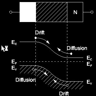
6 pn - junction p n
 n neutrality cond. Maxwell Electric field!")
7 pn junction as particle detector p + n - thin, highly doped p + (~10 19 cm -3 ) layer on lightly doped n - (~10 12 cm -3 ) substrate Space charge region N A de dx x p N D x 1 ( x) n neutrality cond. Maxwell Electric field!! E( x) en en A D ( x x ( x x p n ) ) for for x p x 0 x x n 0 Potential V bi e N 2 A x 2 p N D x 2 n


8 pn junction under reverse bias (V ext ) 1. V bi V bi + V ext 2. no thermal equilibrium => E F (n) E F (p) no bias Hole current Electron current p n forward bias Depletion region Depl. I p n reverse bias Depl. I

9 pn junction as particle detector Depletion zone grows from the junction into the lower doped bulk


10 Metal-semiconductor junction metal semiconductor note work function M depends on type of metal S depends on doping S = electron affinity = E vac E C is independent of doping Schottky Contact =potential barrier i.e e S < e m
11 VORLESUNG 8

12 Silicon Detector (principle sketch)
13 Single sided processing
14 Single sided processing C f - U=Q in / C f + +HV DC - Coupling
15 Single sided processing -HV R bias C f - U=Q in / C f + AC - Coupling

16 Realisation of AC coupling


17 Photolithography n - silicon wafer oxidation at ~1000 C photolithography on SiO 2 p + -doping by ion implantation curing at 600 C, 30 min addition of Al layer lithography on Al oxidised Si wafer coating with photoresist mask exposure of photoresist development edging removal of photoresist

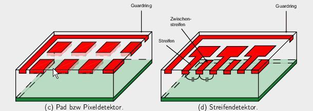
18 Single sided processing

19 Biasing Polysilicon Biasing


20 FOXFET & Punch-Through Biasing V < V pt V V pt Punch Through Biasing V > V pt

21 Biasing of Pixel Detectors Jörn Große-Knetter

22 Double sided readout: insulation problems p + n n +


23 Double sided microstrip detector top side read-out strips bias strips bottom side p-type insulation

24 n-on-n segmentation p-on-n sensor n-on-n sensor Initial undepleted state undepleted After irradiation undepleted undepleted

25 Capacitive charge division


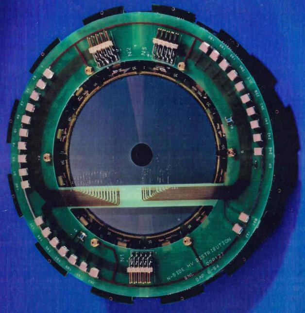
26 Capacitive charge division read Q collected Q incoming particle intermed. strip incoming particle


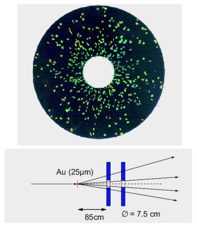
27 - distribution for position-interpolation simple expectation: = Q L /(Q R +Q L ) x = η*d not quite correct, use more complex function:

28 - distribution for position-interpolation ideally symmetric but: parasitic capacitances and r/o specifics intermediate strips intermediate structure in η Jörn Große-Knetter
29 Disturbing effects incoming particle ~300μm -electron reconstr. position effect of -electrons 100 kev -electron occurs in 300 µm Si with 6% probability; has range of 60 µm


30 Disturbing effects measured width of the charge distribution no B-field with B-field influence of Lorentz angle
31 Small pixel effect - II weighting potential for different pixel sizes first central neighbour


32 { Weighting field and signal formation moving charge moving charge signal observed here
33 Sideward Depletion 37


34 Silicon Drift Detectors ~ 10 µm resolution over 5 10 cm drift distances drift velocity must be predictable low trapping problem with radiation damage 38

35 Cylindrical Si-Drift Detector 39
36 40
37 41
38 MONOLITHIC DETECTORS
")
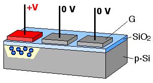
39 MOS (optical) CCD 43
40 s y m m e t r y a x i s 50 µm DEPleted Field Effect Transistor source top gate drain MIP clear bulk Potential distribution: ~1µm p+ + p n+ p+ n+ n n internal gate n - Backcontact Source internal Gate Drain p+ rear contact [TeSCA-Simulation] FET-Transistor integrated in every pixel (first amplification) Electrons are collected in internal gate and modulate the transistor-current Signal charge removed via clear contact 44
 Electrons are collected in internal gate and modulate the transistor-current Signal")
41 s y m m e t r y a x i s 50 µm DEPleted Field Effect Transistor source top gate drain +15 V 0V clear 0V bulk Potential distribution: p+ p n+ p+ n+ n n internal gate Backcontact internal Gate Drain n - Source p+ rear contact [TeSCA-Simulation] FET-Transistor integrated in every pixel (first amplification) Electrons are collected in internal gate and modulate the transistor-current Signal charge removed via clear contact 45

42 Minosa Active PixelS Signal created in low-doped epitaxial layer (typically ~10 μm) Charge sensing in n-well/p-epi junction Charge collection mainly through thermal diffusion (~100 ns), reflective boundaries at p-well and substrate Sensor and signal processing integrated in the same silicon wafer Standard commercial CMOS technology High granularity Fast readout, low noise, low power dissipation 46
 of Hi-R and Low-R Si layers.")


43 SOI Pixel Detector Monolithic detector using Bonded wafer (SOI : Silicon-on-Insulator) of Hi-R and Low-R Si layers. No mechanical bump bondings -> High Density, Low material budget -> Low parasitic Capacitance, High Sensitivity Standard CMOS circuits can be built Thin active Si layer (~40 nm) -> No Latch Up, Small SEE Cross section. Based on Industrial standard technology 47 Seamless connection to Vertical Integration Yasuo Arai 47
 1 Poly, 4 (5) Metal layers, MIM Capacitor, DMOS option Core")
 V Diameter: 200 mm, Top Si : Cz, ~18 -cm, p-type, ~40 nm thick Buried Oxide: 200 nm thick Handle wafer:")
44 OKI 0.2 mm FD-SOI Pixel Process Process SOI wafer Backside 0.2mm Low-Leakage Fully-Depleted SOI CMOS (OKI) 1 Poly, 4 (5) Metal layers, MIM Capacitor, DMOS option Core (I/O) Voltage = 1.8 (3.3) V Diameter: 200 mm, Top Si : Cz, ~18 -cm, p-type, ~40 nm thick Buried Oxide: 200 nm thick Handle wafer: Cz ~700 -cm (n-type), 650 mm thick Thinned to 260 mm and sputtered with Al (200 nm). An example of a SOI Pixel cross section Yasuo Arai 48
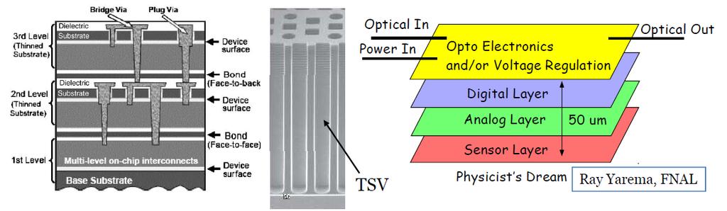
45 3D-Integration
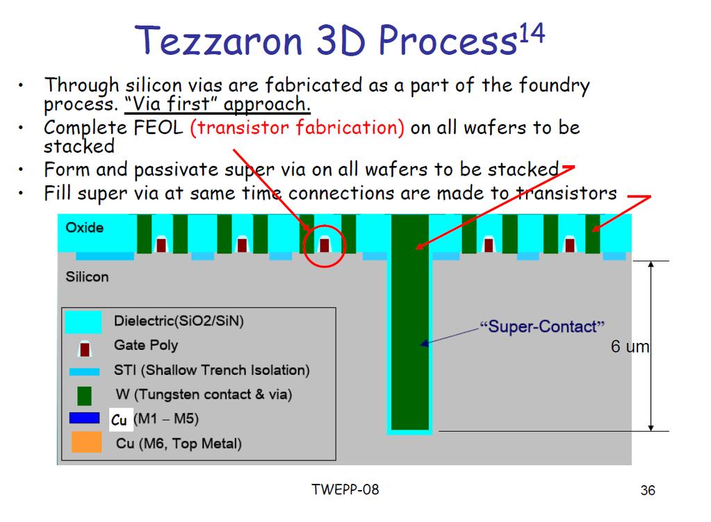
46 3D-Integration R. Yarema
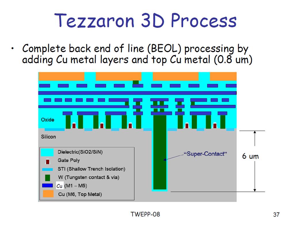
47 3D-Integration
48 3D-Integration
49 3D-Integration
50 3D-Sensors
51 3D-Sensors

52 Enver Alagoz
53 Size of Collider Si-Detectors 54 cm 57

54 ATLAS Silicon Tracker Micro Strip Detector Strips Pixel Detector Pixel 58


55 ATLAS silicon strip detector 60 m 2 of Si, ~4000 modules barrel during module mounting 59

56 Micro Strip Detector 60

57 ATLAS Si-Strip Detector 61


58 CMS silicon strip detector ~19000 modules 250m 2 of Si 62


59 ATLAS pixel module viewed from sensor side MCC sensor flex-hybrid FE-Chip FE-Chip pigtail viewed from chip side 16 IC, pixels
 to interaction point ~10 8")

60 ATLAS pixel detector 1m close (5cm) to interaction point ~10 8 pixels (50x400 µm 2 ) ~1000 pixels hit every 25 ns ASIC Chip Development 64
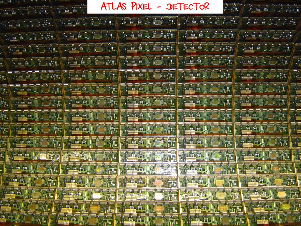
61 ATLAS Pixel-Detector 65
Lecture 18. New gas detectors Solid state trackers
 Lecture 18 New gas detectors Solid state trackers Time projection Chamber Full 3-D track reconstruction x-y from wires and segmented cathode of MWPC z from drift time de/dx information (extra) Drift over
Components of a generic collider detector
 Lecture 24 Components of a generic collider detector electrons - ionization + bremsstrahlung photons - pair production in high Z material charged hadrons - ionization + shower of secondary interactions
Solid State Detectors
 Solid State Detectors Most material is taken from lectures by Michael Moll/CERN and Daniela Bortoletto/Purdue and the book Semiconductor Radiation Detectors by Gerhard Lutz. In gaseous detectors, a charged
Lecture 2. Introduction to semiconductors Structures and characteristics in semiconductors
 Lecture 2 Introduction to semiconductors Structures and characteristics in semiconductors Semiconductor p-n junction Metal Oxide Silicon structure Semiconductor contact Literature Glen F. Knoll, Radiation
Lecture 2. Introduction to semiconductors Structures and characteristics in semiconductors
 Lecture 2 Introduction to semiconductors Structures and characteristics in semiconductors Semiconductor p-n junction Metal Oxide Silicon structure Semiconductor contact Literature Glen F. Knoll, Radiation
Semiconductor Detectors
 Semiconductor Detectors Summary of Last Lecture Band structure in Solids: Conduction band Conduction band thermal conductivity: E g > 5 ev Valence band Insulator Charge carrier in conductor: e - Charge
Semiconductor-Detectors
 Semiconductor-Detectors 1 Motivation ~ 195: Discovery that pn-- junctions can be used to detect particles. Semiconductor detectors used for energy measurements ( Germanium) Since ~ 3 years: Semiconductor
Peter Fischer, ziti, Universität Heidelberg. Silicon Detectors & Readout Electronics
 Silicon Detectors and Readout Electronics Peter Fischer, ziti, Universität Heidelberg 1 Content of the Lecture (sorted by subject) Introduction: Applications of silicon detectors Requirements, measured
Midterm I - Solutions
 UNIVERSITY OF CALIFORNIA College of Engineering Department of Electrical Engineering and Computer Sciences EECS 130 Spring 2008 Professor Chenming Hu Midterm I - Solutions Name: SID: Grad/Undergrad: Closed
Silicon Detectors in High Energy Physics
 Thomas Bergauer (HEPHY Vienna) IPM Teheran 22 May 2011 Sunday: Schedule Silicon Detectors in Semiconductor Basics (45 ) Detector concepts: Pixels and Strips (45 ) Coffee Break Strip Detector Performance
Final Examination EE 130 December 16, 1997 Time allotted: 180 minutes
 Final Examination EE 130 December 16, 1997 Time allotted: 180 minutes Problem 1: Semiconductor Fundamentals [30 points] A uniformly doped silicon sample of length 100µm and cross-sectional area 100µm 2
Section 12: Intro to Devices
 Section 12: Intro to Devices Extensive reading materials on reserve, including Robert F. Pierret, Semiconductor Device Fundamentals Bond Model of Electrons and Holes Si Si Si Si Si Si Si Si Si Silicon
Lecture 2. Introduction to semiconductors Structures and characteristics in semiconductors. Fabrication of semiconductor sensor
 Lecture 2 Introduction to semiconductors Structures and characteristics in semiconductors Semiconductor p-n junction Metal Oxide Silicon structure Semiconductor contact Fabrication of semiconductor sensor
Lecture 12: MOS Capacitors, transistors. Context
 Lecture 12: MOS Capacitors, transistors Context In the last lecture, we discussed PN diodes, and the depletion layer into semiconductor surfaces. Small signal models In this lecture, we will apply those
Lecture 150 Basic IC Processes (10/10/01) Page ECE Analog Integrated Circuits and Systems P.E. Allen
 Page ECE Analog Integrated Circuits and Systems P.E. Allen") Lecture 150 Basic IC Processes (10/10/01) Page 1501 LECTURE 150 BASIC IC PROCESSES (READING: TextSec. 2.2) INTRODUCTION Objective The objective of this presentation is: 1.) Introduce the fabrication of
Lecture 150 Basic IC Processes (10/10/01) Page 1501 LECTURE 150 BASIC IC PROCESSES (READING: TextSec. 2.2) INTRODUCTION Objective The objective of this presentation is: 1.) Introduce the fabrication of
DEPFET sensors development for the Pixel Detector of BELLE II
 DEPFET sensors development for the Pixel Detector of BELLE II 13 th Topical Seminar on Innovative Particle and Radiation Detectors (IPRD13) 7 10 October 2013, Siena, Italy Paola Avella for the DEPFET collaboration
Solid State Detectors Semiconductor detectors Halbleiterdetektoren
 Solid State Detectors Semiconductor detectors Halbleiterdetektoren Doris Eckstein DESY Where are solid state detectors used? > Nuclear Physics: Energy measurement of charged particles (particles up to
Development of Radiation Hard Si Detectors
 Development of Radiation Hard Si Detectors Dr. Ajay K. Srivastava On behalf of Detector Laboratory of the Institute for Experimental Physics University of Hamburg, D-22761, Germany. Ajay K. Srivastava
Chap. 11 Semiconductor Diodes
 Chap. 11 Semiconductor Diodes Semiconductor diodes provide the best resolution for energy measurements, silicon based devices are generally used for charged-particles, germanium for photons. Scintillators
Classification of Solids
 Classification of Solids Classification by conductivity, which is related to the band structure: (Filled bands are shown dark; D(E) = Density of states) Class Electron Density Density of States D(E) Examples
Radiation Detector 2016/17 (SPA6309)
") Radiation Detector 2016/17 (SPA6309) Semiconductor detectors (Leo, Chapter 10) 2017 Teppei Katori Semiconductor detectors are used in many situations, mostly for some kind of high precision measurement.
Radiation Detector 2016/17 (SPA6309) Semiconductor detectors (Leo, Chapter 10) 2017 Teppei Katori Semiconductor detectors are used in many situations, mostly for some kind of high precision measurement.
SILICON PARTICLE DETECTOR
 SILICON PARTICLE DETECTOR Supervised Learning Project Eslikumar Adiandhra 12D260012 Department of Physics, IIT Bombay Guide: Prof. Raghava Varma Department of Physics, IIT Bombay November 8, 2015 Abstract
Tracking detectors for the LHC. Peter Kluit (NIKHEF)
") Tracking detectors for the LHC Peter Kluit (NIKHEF) Overview lectures part I Principles of gaseous and solid state tracking detectors Tracking detectors at the LHC Drift chambers Silicon detectors Modeling
Tracking detectors for the LHC Peter Kluit (NIKHEF) Overview lectures part I Principles of gaseous and solid state tracking detectors Tracking detectors at the LHC Drift chambers Silicon detectors Modeling
Semiconductor Detectors are Ionization Chambers. Detection volume with electric field Energy deposited positive and negative charge pairs
 1 V. Semiconductor Detectors V.1. Principles Semiconductor Detectors are Ionization Chambers Detection volume with electric field Energy deposited positive and negative charge pairs Charges move in field
an introduction to Semiconductor Devices
 an introduction to Semiconductor Devices Donald A. Neamen Chapter 6 Fundamentals of the Metal-Oxide-Semiconductor Field-Effect Transistor Introduction: Chapter 6 1. MOSFET Structure 2. MOS Capacitor -
Fundamentals of the Metal Oxide Semiconductor Field-Effect Transistor
 Triode Working FET Fundamentals of the Metal Oxide Semiconductor Field-Effect Transistor The characteristics of energy bands as a function of applied voltage. Surface inversion. The expression for the
Schottky Rectifiers Zheng Yang (ERF 3017,
 ECE442 Power Semiconductor Devices and Integrated Circuits Schottky Rectifiers Zheng Yang (ERF 3017, email: yangzhen@uic.edu) Power Schottky Rectifier Structure 2 Metal-Semiconductor Contact The work function
ELEN0037 Microelectronic IC Design. Prof. Dr. Michael Kraft
 ELEN0037 Microelectronic IC Design Prof. Dr. Michael Kraft Lecture 2: Technological Aspects Technology Passive components Active components CMOS Process Basic Layout Scaling CMOS Technology Integrated
ESE 570: Digital Integrated Circuits and VLSI Fundamentals
 ESE 570: Digital Integrated Circuits and VLSI Fundamentals Lec 4: January 23, 2018 MOS Transistor Theory, MOS Model Penn ESE 570 Spring 2018 Khanna Lecture Outline! CMOS Process Enhancements! Semiconductor
Lecture 0: Introduction
 Lecture 0: Introduction Introduction q Integrated circuits: many transistors on one chip q Very Large Scale Integration (VLSI): bucketloads! q Complementary Metal Oxide Semiconductor Fast, cheap, low power
Chapter 2. Design and Fabrication of VLSI Devices
 Chapter 2 Design and Fabrication of VLSI Devices Jason Cong 1 Design and Fabrication of VLSI Devices Objectives: To study the materials used in fabrication of VLSI devices. To study the structure of devices
Semiconductor X-Ray Detectors. Tobias Eggert Ketek GmbH
 Semiconductor X-Ray Detectors Tobias Eggert Ketek GmbH Semiconductor X-Ray Detectors Part A Principles of Semiconductor Detectors 1. Basic Principles 2. Typical Applications 3. Planar Technology 4. Read-out
Section 12: Intro to Devices
 Section 12: Intro to Devices Extensive reading materials on reserve, including Robert F. Pierret, Semiconductor Device Fundamentals EE143 Ali Javey Bond Model of Electrons and Holes Si Si Si Si Si Si Si
UNIVERSITY OF CALIFORNIA College of Engineering Department of Electrical Engineering and Computer Sciences. EECS 130 Professor Ali Javey Fall 2006
 UNIVERSITY OF CALIFORNIA College of Engineering Department of Electrical Engineering and Computer Sciences EECS 130 Professor Ali Javey Fall 2006 Midterm 2 Name: SID: Closed book. Two sheets of notes are
Chapter 3 Basics Semiconductor Devices and Processing
 Chapter 3 Basics Semiconductor Devices and Processing Hong Xiao, Ph. D. www2.austin.cc.tx.us/hongxiao/book.htm Hong Xiao, Ph. D. www2.austin.cc.tx.us/hongxiao/book.htm 1 Objectives Identify at least two
MOSFET: Introduction
 E&CE 437 Integrated VLSI Systems MOS Transistor 1 of 30 MOSFET: Introduction Metal oxide semiconductor field effect transistor (MOSFET) or MOS is widely used for implementing digital designs Its major
Lecture 6 PN Junction and MOS Electrostatics(III) Metal-Oxide-Semiconductor Structure
 Metal-Oxide-Semiconductor Structure") Lecture 6 PN Junction and MOS Electrostatics(III) Metal-Oxide-Semiconductor Structure Outline 1. Introduction to MOS structure 2. Electrostatics of MOS in thermal equilibrium 3. Electrostatics of MOS with
Lecture 6 PN Junction and MOS Electrostatics(III) Metal-Oxide-Semiconductor Structure Outline 1. Introduction to MOS structure 2. Electrostatics of MOS in thermal equilibrium 3. Electrostatics of MOS with
Advantages / Disadvantages of semiconductor detectors
 Advantages / Disadvantages of semiconductor detectors Semiconductor detectors have a high density (compared to gas detector) large energy loss in a short distance diffusion effect is smaller than in gas
1 Name: Student number: DEPARTMENT OF PHYSICS AND PHYSICAL OCEANOGRAPHY MEMORIAL UNIVERSITY OF NEWFOUNDLAND. Fall :00-11:00
 1 Name: DEPARTMENT OF PHYSICS AND PHYSICAL OCEANOGRAPHY MEMORIAL UNIVERSITY OF NEWFOUNDLAND Final Exam Physics 3000 December 11, 2012 Fall 2012 9:00-11:00 INSTRUCTIONS: 1. Answer all seven (7) questions.
MENA9510 characterization course: Capacitance-voltage (CV) measurements
 measurements") MENA9510 characterization course: Capacitance-voltage (CV) measurements 30.10.2017 Halvard Haug Outline Overview of interesting sample structures Ohmic and schottky contacts Why C-V for solar cells? The
MENA9510 characterization course: Capacitance-voltage (CV) measurements 30.10.2017 Halvard Haug Outline Overview of interesting sample structures Ohmic and schottky contacts Why C-V for solar cells? The
EE115C Winter 2017 Digital Electronic Circuits. Lecture 3: MOS RC Model, CMOS Manufacturing
 EE115C Winter 2017 Digital Electronic Circuits Lecture 3: MOS RC Model, CMOS Manufacturing Agenda MOS Transistor: RC Model (pp. 104-113) S R on D CMOS Manufacturing Process (pp. 36-46) S S C GS G G C GD
ESE 570: Digital Integrated Circuits and VLSI Fundamentals
 ESE 570: Digital Integrated Circuits and VLSI Fundamentals Lec 4: January 29, 2019 MOS Transistor Theory, MOS Model Penn ESE 570 Spring 2019 Khanna Lecture Outline! CMOS Process Enhancements! Semiconductor
EE 5344 Introduction to MEMS CHAPTER 5 Radiation Sensors
 EE 5344 Introduction to MEMS CHAPTER 5 Radiation Sensors 5. Radiation Microsensors Radiation µ-sensors convert incident radiant signals into standard electrical out put signals. Radiant Signals Classification
The Devices: MOS Transistors
 The Devices: MOS Transistors References: Semiconductor Device Fundamentals, R. F. Pierret, Addison-Wesley Digital Integrated Circuits: A Design Perspective, J. Rabaey et.al. Prentice Hall NMOS Transistor
Session 6: Solid State Physics. Diode
 Session 6: Solid State Physics Diode 1 Outline A B C D E F G H I J 2 Definitions / Assumptions Homojunction: the junction is between two regions of the same material Heterojunction: the junction is between
Spring Semester 2012 Final Exam
 Spring Semester 2012 Final Exam Note: Show your work, underline results, and always show units. Official exam time: 2.0 hours; an extension of at least 1.0 hour will be granted to anyone. Materials parameters
EE382M-14 CMOS Analog Integrated Circuit Design
 EE382M-14 CMOS Analog Integrated Circuit Design Lecture 3, MOS Capacitances, Passive Components, and Layout of Analog Integrated Circuits MOS Capacitances Type of MOS transistor capacitors Depletion capacitance
Lecture 210 Physical Aspects of ICs (12/15/01) Page 210-1
 Page 210-1") Lecture 210 Physical Aspects of ICs (12/15/01) Page 210-1 LECTURE 210 PHYSICAL ASPECTS OF ICs (READING: Text-Sec. 2.5, 2.6, 2.8) INTRODUCTION Objective Illustrate the physical aspects of integrated circuits
Lecture 210 Physical Aspects of ICs (12/15/01) Page 210-1 LECTURE 210 PHYSICAL ASPECTS OF ICs (READING: Text-Sec. 2.5, 2.6, 2.8) INTRODUCTION Objective Illustrate the physical aspects of integrated circuits
Lecture 4. Detectors for Ionizing Particles
 Lecture 4 Detectors for Ionizing Particles Introduction Overview of detector systems Sources of radiation Radioactive decay Cosmic Radiation Accelerators Content Interaction of Radiation with Matter General
Chapter 8 Ion Implantation
 Chapter 8 Ion Implantation 2006/5/23 1 Wafer Process Flow Materials IC Fab Metalization CMP Dielectric deposition Test Wafers Masks Thermal Processes Implant PR strip Etch PR strip Packaging Photolithography
Energetic particles and their detection in situ (particle detectors) Part II. George Gloeckler
 Part II. George Gloeckler") Energetic particles and their detection in situ (particle detectors) Part II George Gloeckler University of Michigan, Ann Arbor, MI University of Maryland, College Park, MD Simple particle detectors Gas-filled
Energetic particles and their detection in situ (particle detectors) Part II George Gloeckler University of Michigan, Ann Arbor, MI University of Maryland, College Park, MD Simple particle detectors Gas-filled
! CMOS Process Enhancements. ! Semiconductor Physics. " Band gaps. " Field Effects. ! MOS Physics. " Cut-off. " Depletion.
 ESE 570: Digital Integrated Circuits and VLSI Fundamentals Lec 4: January 3, 018 MOS Transistor Theory, MOS Model Lecture Outline! CMOS Process Enhancements! Semiconductor Physics " Band gaps " Field Effects!
Review of Semiconductor Drift Detectors
 Pavia October 25, 2004 Review of Semiconductor Drift Detectors Talk given by Pavel Rehak following a presentation on 5 th Hiroshima Symposium of Semiconductor Tracking Detectors Outline of the Review Principles
Semiconductor Physics fall 2012 problems
 Semiconductor Physics fall 2012 problems 1. An n-type sample of silicon has a uniform density N D = 10 16 atoms cm -3 of arsenic, and a p-type silicon sample has N A = 10 15 atoms cm -3 of boron. For each
Self-study problems and questions Processing and Device Technology, FFF110/FYSD13
 Self-study problems and questions Processing and Device Technology, FFF110/FYSD13 Version 2016_01 In addition to the problems discussed at the seminars and at the lectures, you can use this set of problems
Lecture 7 MOS Capacitor
 EE 471: Transport Phenomena in Solid State Devices Spring 2018 Lecture 7 MOS Capacitor Bryan Ackland Department of Electrical and Computer Engineering Stevens Institute of Technology Hoboken, NJ 07030
D. Meier. representing the RD42 Collaboration. Bristol University, CERN, CPP Marseille, Lawrence Livermore National Lab, LEPSI
 Diamond as a Particle Detector D. Meier representing the RD42 Collaboration Bristol University, CERN, CPP Marseille, Lawrence Livermore National Lab, LEPSI Strasbourg, Los Alamos National Lab, MPIK Heidelberg,
MOS Transistor I-V Characteristics and Parasitics
 ECEN454 Digital Integrated Circuit Design MOS Transistor I-V Characteristics and Parasitics ECEN 454 Facts about Transistors So far, we have treated transistors as ideal switches An ON transistor passes
Semiconductor Physics Problems 2015
 Semiconductor Physics Problems 2015 Page and figure numbers refer to Semiconductor Devices Physics and Technology, 3rd edition, by SM Sze and M-K Lee 1. The purest semiconductor crystals it is possible
Scaling Issues in Planar FET: Dual Gate FET and FinFETs
 Scaling Issues in Planar FET: Dual Gate FET and FinFETs Lecture 12 Dr. Amr Bayoumi Fall 2014 Advanced Devices (EC760) Arab Academy for Science and Technology - Cairo 1 Outline Scaling Issues for Planar
CMOS Devices. PN junctions and diodes NMOS and PMOS transistors Resistors Capacitors Inductors Bipolar transistors
 CMOS Devices PN junctions and diodes NMOS and PMOS transistors Resistors Capacitors Inductors Bipolar transistors PN Junctions Diffusion causes depletion region D.R. is insulator and establishes barrier
Physics of Semiconductors 8 th
 Physics of Semiconductors 8 th 2016.6.6 Shingo Katsumoto Department of Physics, Institute for Solid State Physics University of Tokyo Review of pn junction Estimation of builtin potential Depletion layer
Silicon Detectors in High Energy Physics
 Thomas Bergauer (HEPHY Vienna) IPM Teheran 22 May 2011 Sunday: Schedule Semiconductor Basics (45 ) Silicon Detectors in Detector concepts: Pixels and Strips (45 ) Coffee Break Strip Detector Performance
Dr. Maria-Alexandra PAUN
 Performance comparison of Hall Effect Sensors obtained by regular bulk or SOI CMOS technology Dr. Maria-Alexandra PAUN Visiting Researcher High Voltage Microelectronics and Sensors (HVMS) Group, Department
Seminar talks. Overall description of CLAS12 (Jefferson Lab) MAPS. Talks on Feb. 6 th, (Contact JR) (Contact TS)
 MAPS. Talks on Feb. 6 th, (Contact JR) (Contact TS)") Seminar talks Overall description of CLAS12 (Jefferson Lab) (Contact JR) MAPS (Contact TS) Talks on Feb. 6 th, 2015 Review old ionization detectors: Emulsion, Cloud chambers, Ionization chambers, Spark
Seminar talks Overall description of CLAS12 (Jefferson Lab) (Contact JR) MAPS (Contact TS) Talks on Feb. 6 th, 2015 Review old ionization detectors: Emulsion, Cloud chambers, Ionization chambers, Spark
Electrical Characteristics of MOS Devices
 Electrical Characteristics of MOS Devices The MOS Capacitor Voltage components Accumulation, Depletion, Inversion Modes Effect of channel bias and substrate bias Effect of gate oide charges Threshold-voltage
Operation and Modeling of. The MOS Transistor. Second Edition. Yannis Tsividis Columbia University. New York Oxford OXFORD UNIVERSITY PRESS
 Operation and Modeling of The MOS Transistor Second Edition Yannis Tsividis Columbia University New York Oxford OXFORD UNIVERSITY PRESS CONTENTS Chapter 1 l.l 1.2 1.3 1.4 1.5 1.6 1.7 Chapter 2 2.1 2.2
Photodetector. Prof. Woo-Young Choi. Silicon Photonics (2012/2) Photodetection: Absorption => Current Generation. Currents
 Photodetection: Absorption => Current Generation. Currents") Photodetection: Absorption => Current Generation h Currents Materials for photodetection: E g < h Various methods for generating currents with photo-generated carriers: photoconductors, photodiodes, avalanche
Photodetection: Absorption => Current Generation h Currents Materials for photodetection: E g < h Various methods for generating currents with photo-generated carriers: photoconductors, photodiodes, avalanche
EE 4345 Chapter 6. Derek Johnson Michael Hasni Rex Reeves Michael Custer
 EE 4345 Chapter 6 Derek Johnson Michael Hasni Rex Reeves Michael Custer Coupling AC Signals Constructing timing networks Constructing phase shift networks Feedback loop compensation Semiconductors use:
Class 05: Device Physics II
 Topics: 1. Introduction 2. NFET Model and Cross Section with Parasitics 3. NFET as a Capacitor 4. Capacitance vs. Voltage Curves 5. NFET as a Capacitor - Band Diagrams at V=0 6. NFET as a Capacitor - Accumulation
ECE-305: Fall 2017 Metal Oxide Semiconductor Devices
 C-305: Fall 2017 Metal Oxide Semiconductor Devices Pierret, Semiconductor Device Fundamentals (SDF) Chapters 15+16 (pp. 525-530, 563-599) Professor Peter Bermel lectrical and Computer ngineering Purdue
CMPEN 411 VLSI Digital Circuits. Lecture 03: MOS Transistor
 CMPEN 411 VLSI Digital Circuits Lecture 03: MOS Transistor Kyusun Choi [Adapted from Rabaey s Digital Integrated Circuits, Second Edition, 2003 J. Rabaey, A. Chandrakasan, B. Nikolic] CMPEN 411 L03 S.1
! CMOS Process Enhancements. ! Semiconductor Physics. " Band gaps. " Field Effects. ! MOS Physics. " Cut-off. " Depletion.
 ESE 570: Digital Integrated Circuits and VLSI Fundamentals Lec 4: January 9, 019 MOS Transistor Theory, MOS Model Lecture Outline CMOS Process Enhancements Semiconductor Physics Band gaps Field Effects
Tracking in High Energy Physics: Silicon Devices!
 Tracking in High Energy Physics: Silicon Devices! G. Leibenguth XIX Graduiertenkolleg Heidelberg 11-12. October 2007 Content Part 1: Basics on semi-conductor Part 2: Construction Part 3: Two Examples Part
Status Report: Charge Cloud Explosion
 Status Report: Charge Cloud Explosion J. Becker, D. Eckstein, R. Klanner, G. Steinbrück University of Hamburg Detector laboratory 1. Introduction and Motivation. Set-up available for measurement 3. Measurements
Introduction to Silicon Detectors. G.Villani STFC Rutherford Appleton Laboratory Particle Physics Department
 Introduction to Silicon Detectors G.Villani STFC Rutherford Appleton Laboratory Particle Physics Department 1 Outlook Introduction to physics of Si and detection Examples of detectors Radiation effects
R. Ludwig and G. Bogdanov RF Circuit Design: Theory and Applications 2 nd edition. Figures for Chapter 6
 R. Ludwig and G. Bogdanov RF Circuit Design: Theory and Applications 2 nd edition Figures for Chapter 6 Free electron Conduction band Hole W g W C Forbidden Band or Bandgap W V Electron energy Hole Valence
EECS130 Integrated Circuit Devices
 EECS130 Integrated Circuit Devices Professor Ali Javey 10/02/2007 MS Junctions, Lecture 2 MOS Cap, Lecture 1 Reading: finish chapter14, start chapter16 Announcements Professor Javey will hold his OH at
UNIVERSITY OF CALIFORNIA College of Engineering Department of Electrical Engineering and Computer Sciences. Professor Chenming Hu.
 UNIVERSITY OF CALIFORNIA College of Engineering Department of Electrical Engineering and Computer Sciences EECS 130 Spring 2009 Professor Chenming Hu Midterm I Name: Closed book. One sheet of notes is
nmos IC Design Report Module: EEE 112
 nmos IC Design Report Author: 1302509 Zhao Ruimin Module: EEE 112 Lecturer: Date: Dr.Zhao Ce Zhou June/5/2015 Abstract This lab intended to train the experimental skills of the layout designing of the
The Intrinsic Silicon
 The Intrinsic ilicon Thermally generated electrons and holes Carrier concentration p i =n i ni=1.45x10 10 cm-3 @ room temp Generally: n i = 3.1X10 16 T 3/2 e -1.21/2KT cm -3 T= temperature in K o (egrees
MOSFET SCALING ECE 663
 MOSFET SCALING Scaling of switches Moore s Law economics Moore s Law - #DRAM Bits per chip doubles every 18 months ~5% bigger chips/wafers ~5% design improvements ~50 % Lithography ability to print smaller
The ATLAS Silicon Microstrip Tracker
 9th 9th Topical Seminar on Innovative Particle and Radiation Detectors 23-26 May 2004 Siena3 The ATLAS Silicon Microstrip Tracker Zdenek Dolezal, Charles University at Prague, for the ATLAS SCT Collaboration
GaN based transistors
 GaN based transistors S FP FP dielectric G SiO 2 Al x Ga 1-x N barrier i-gan Buffer i-sic D Transistors "The Transistor was probably the most important invention of the 20th Century The American Institute
GEM at CERN. Leszek Ropelewski CERN PH-DT2 DT2-ST & TOTEM
 GEM at CERN Leszek Ropelewski CERN PH-DT2 DT2-ST & TOTEM MicroStrip Gas Chamber Semiconductor industry technology: Photolithography Etching Coating Doping A. Oed Nucl. Instr. and Meth. A263 (1988) 351.
The Devices. Digital Integrated Circuits A Design Perspective. Jan M. Rabaey Anantha Chandrakasan Borivoje Nikolic. July 30, 2002
 Digital Integrated Circuits A Design Perspective Jan M. Rabaey Anantha Chandrakasan Borivoje Nikolic The Devices July 30, 2002 Goal of this chapter Present intuitive understanding of device operation Introduction
Circuits. L5: Fabrication and Layout -2 ( ) B. Mazhari Dept. of EE, IIT Kanpur. B. Mazhari, IITK. G-Number
 B. Mazhari Dept. of EE, IIT Kanpur. B. Mazhari, IITK. G-Number") EE610: CMOS Analog Circuits L5: Fabrication and Layout -2 (12.8.2013) B. Mazhari Dept. of EE, IIT Kanpur 44 Passive Components: Resistor Besides MOS transistors, sometimes one requires to implement passive
EE610: CMOS Analog Circuits L5: Fabrication and Layout -2 (12.8.2013) B. Mazhari Dept. of EE, IIT Kanpur 44 Passive Components: Resistor Besides MOS transistors, sometimes one requires to implement passive
Lecture 15 OUTLINE. MOSFET structure & operation (qualitative) Review of electrostatics The (N)MOS capacitor
 Review of electrostatics The (N)MOS capacitor") Lecture 15 OUTLINE MOSFET structure & operation (qualitative) Review of electrostatics The (N)MOS capacitor Electrostatics t ti Charge vs. voltage characteristic Reading: Chapter 6.1 6.2.1 EE105 Fall 2007
Lecture 15 OUTLINE MOSFET structure & operation (qualitative) Review of electrostatics The (N)MOS capacitor Electrostatics t ti Charge vs. voltage characteristic Reading: Chapter 6.1 6.2.1 EE105 Fall 2007
Theory of Electrical Characterization of Semiconductors
 Theory of Electrical Characterization of Semiconductors P. Stallinga Universidade do Algarve U.C.E.H. A.D.E.E.C. OptoElectronics SELOA Summer School May 2000, Bologna (It) Overview Devices: bulk Schottky
Quiz #1 Practice Problem Set
 Name: Student Number: ELEC 3908 Physical Electronics Quiz #1 Practice Problem Set? Minutes January 22, 2016 - No aids except a non-programmable calculator - All questions must be answered - All questions
MOS Transistor Properties Review
 MOS Transistor Properties Review 1 VLSI Chip Manufacturing Process Photolithography: transfer of mask patterns to the chip Diffusion or ion implantation: selective doping of Si substrate Oxidation: SiO
Aspects of radiation hardness for silicon microstrip detectors
 Aspects of radiation hardness for silicon microstrip detectors Richard Wheadon, INFN Pisa, Via Livornese 1291, S. Piero a Grado, Pisa, Italy Abstract The ways in which radiation damage affects the properties
Challenges for Silicon Pixel Sensors at the XFEL. Table of Content
 Challenges for Silicon Pixel Sensors at the XFEL R.Klanner (Inst. Experimental Physics, Hamburg University) work by J.Becker, E.Fretwurst, I.Pintilie, T.Pöhlsen, J.Schwandt, J.Zhang Table of Content 1.Introduction:
1) CMOS-Sensors for vertex-detectors 2) CMOS-Sensors for X-ray imaging 3) Sensor with a 3-T-preamplifier 4) Sensor with nearly full depletion
 CMOS-Sensors for vertex-detectors 2) CMOS-Sensors for X-ray imaging 3) Sensor with a 3-T-preamplifier 4) Sensor with nearly full depletion") AD vanced MO nolithic ensors for S CMOS-sensors for energy-resolved X-ray imaging Dennis Doering, Samir Amar, Jerome Baudot², Michael Deveaux, Wojciech Dulinski², Maciej Kachel², Tomasz Hemperek³, Christian
AD vanced MO nolithic ensors for S CMOS-sensors for energy-resolved X-ray imaging Dennis Doering, Samir Amar, Jerome Baudot², Michael Deveaux, Wojciech Dulinski², Maciej Kachel², Tomasz Hemperek³, Christian
Future trends in radiation hard electronics
 Future trends in radiation hard electronics F. Faccio CERN, Geneva, Switzerland Outline Radiation effects in CMOS technologies Deep submicron CMOS for radiation environments What is the future going to
Integrated Circuits & Systems
 Federal University of Santa Catarina Center for Technology Computer Science & Electronics Engineering Integrated Circuits & Systems INE 5442 Lecture 10 MOSFET part 1 guntzel@inf.ufsc.br ual-well Trench-Isolated
Experimental Particle Physics
 Experimental Particle Physics Particle Interactions and Detectors Lecture 2 2nd May 2014 Fergus Wilson, RAL 1/31 How do we detect particles? Particle Types Charged (e - /K - /π - ) Photons (γ) Electromagnetic
Semiconductor Physics fall 2012 problems
 Semiconductor Physics fall 2012 problems 1. An n-type sample of silicon has a uniform density N D = 10 16 atoms cm -3 of arsenic, and a p-type silicon sample has N A = 10 15 atoms cm -3 of boron. For each
Introduction and Background
 Analog CMOS Integrated Circuit Design Introduction and Background Dr. Jawdat Abu-Taha Department of Electrical and Computer Engineering Islamic University of Gaza jtaha@iugaza.edu.ps 1 Marking Assignments
Development of High-Z Semiconductor Detectors and Their Applications to X-ray/gamma-ray Astronomy
 Development of High-Z Semiconductor Detectors and Their Applications to X-ray/gamma-ray Astronomy Taka Tanaka (SLAC/KIPAC) 9/19/2007 SLAC Advanced Instrumentation Seminar Outline Introduction CdTe Diode