Advantages / Disadvantages of semiconductor detectors
|
|
|
- Bryce Alexander
- 6 years ago
- Views:
Transcription
1 Advantages / Disadvantages of semiconductor detectors Semiconductor detectors have a high density (compared to gas detector) large energy loss in a short distance diffusion effect is smaller than in gas detectors resulting in achievable position resolution of less then 10 μm Low ionization energy (few ev per e hole pair) compared to gas detectors (20 40 ev per e ion pair) or scintillators ( ev to create a photon) No internal amplification, i.e. small signal with a few exceptions High cost per surface unit not only Silicon itself high number of readout channels large power consumption, cooling
2 Elemental Semiconductor Germanium: used in nuclear physics needs cooling due to small band gap of 0.66 ev (usually done with liquid nitrogen at 77 K) Silicon: can be operated at room temperature synergies with micro electronics industry Diamond (CVD or single crystal): allotrope of carbon large band gap (requires no depletion zone) very radiation hard disadvanture: low signal and high cost
, III V (e.g. GaAs) II VI compounds (CdTe, ZnSe) important III V compounds: GaAs: faster and probably more radiation resistant than Si.")
3 Compound semiconductors Compound semiconductors consist of two (binary semiconductors) or more than two Depending on the column in the periodic system of elements one differentiates between IV IV (e.g. SiGe, SiC), III V (e.g. GaAs) II VI compounds (CdTe, ZnSe) important III V compounds: GaAs: faster and probably more radiation resistant than Si. Drawback is less experience in industry and higher costs. GaP, GaSb, InP, InAs, InSb, InAIP important II VI compounds: CdTe: high atomic number ( ) hence very efficient to detect photons. ZnS, ZnSe, ZnTe, CdS, Cd 1-x Zn x Te, Cd 1-x Zn x Se
4 Why Silicon Semiconductor with moderate bandgap (1.12 ev) Energy to create electron/hole pair (signal quanta) = 3.6 ev (c.f. Argon gas = 15 ev) high carrier yield better energy resolution and high signal no gain stage required plus phonon excitation High density and atomic number higher specific energy loss thinner detectors reduced range of secondary particles better spatial resolution High carrier mobility Fast! less than 30 ns to collect entire signal Large experience in industry with micro-chip technology High intrinsic radiation hardness
5 Bond model of semiconductors Example of column IV elemental semiconductor (2-dimensional projection): Each atom has 4 closest neighbors, the 4 electrons in the outer shell are shared and form covalent bonds. At low temperature all electrons are bound At higher temperature thermal vibrations break some of the bonds free e - cause conductivity (electron conduction) The remaining open bonds attract other e - the holes change position (hole conduction)
.")
6 Energy bands: isolator semiconductor - metal In an isolated atom the electrons have only discrete energy levels. In solid state material the atomic levels merge to energy bands. In metals the conduction and the valence band overlap, whereas in isolators and semiconductors these levels are separated by an energy gap (band gap). In isolators this gap is large.

7 Fermi distribution, Fermi levels Fermi distribution ff EE describes the probability that an electronic state with energy E is occupied by an electron ff EE = ee EE EE FF kkkk The Fermi level E F is the energy at which the probability of occupation is 50%. For metals E F is in the conduction band, for semiconductors and isolators E F is in the band gap Fermi distribution function for different temperatures T 4 > T 3 > T 2 > T 1 > T 0 = 0 K T 0 = 0 K: saltus function

8 Intrinsic semi-conductor properties Dispersion relation EE kk = ħ2 kk 2 2mm ee = ħ2 2mm ee kk xx 2 + kk yy 2 + kk zz 2 Density of states gg EE = dddd dddd = EE1 2 2mm ee ħ VV 2ππ 2 Fermi-Dirac distribution ff EE, TT = ee EE μμ Electron density 1 kk BBTT + 1 nn = 1 EE mmmmmm VV gg EE ff EE dddd 0
9 Drift velocity and mobility Drift velocity for electrones: vv nn = μμ nn EE and for holes: vv pp = μμ pp EE Mobility for electrones: μμ nn = ee ττ nn mm nn and for holes: μμ pp = ee ττ pp mm pp
10 Resistivity Specific resistivity is a measure of silicon purity Carrier mobilities: μ p (Si, 300K) 450 cm 2 /Vs μ n (Si, 300K) 1450 cm 2 /Vs The charge carrier concentration in pure silicon (i.e. intrinsic Si) for T = 300 K is: n e = n h cm -3 This yields an intrinsic resistivity of: ρ 230 kωcm

11 Comparison of different semiconductor materials

12 Comparison of different semiconductor materials
13 Constructing a detector One of the most important parameter of a detector is the signal-to-noise-ratio (SNR). A good detector should have a large SNR. However this leads to two contradictory requirements: Large signal low ionization energy small band gap Low noise very few intrinsic charge carriers large band gap An optimal material should have E g 6 ev In this case the conduction band is almost empty at room temperature and the band gap is small enough to create a large number of e - h + pairs through ionization. Such a material exist, it is Diamond. However even even artificial diamonds (e.g. CVD diamonds) are too expensive for large area detectors.
14 Constructing a detector Let s make a simple calculation for silicon: mean ionization energy I 0 = 3.62 ev. mean energy loss per flight path of a mip de/dx = 3.87 MeV/cm Assuming a detector with a thickness of d = 300 μm and an area of A = 1 cm 2 Signal of a mip in such a detector: dddd dddd dd II 0 = eeee cccc 0.03cccc ee h + pppppppppp 3.62eeee Intrinsic charge carrier in the same volume (T = 300 K) nn ii dd AA = cccc cccc 1cccc ee h + pppppppppp Result: the number of thermal created e-h+-pairs (noise is four orders of magnitude larger than the signal. We have to remove the charge carriers depletion zone in inverse biased pn junctions
15 Doping A pn junction consists of n and p doped substrates: Doping is the replacement of a small number of atoms in the lattice by atoms of neighboring columns from the periodic table These doping atoms create energy levels within the band gap and therefore alter the conductivity. Definitions: An un-doped semiconductor is called an intrinsic semiconductor For each conduction electron exists the corresponding hole. A doped semiconductor is called an extrinsic semiconductor. Extrinsic semiconductors have a abundance of electrons or holes.
16 Doping: n- and p-type silicon
17 Bond model: n-doping in silicon Doping with an element 5 atom (e.g. P, As, Sb). The 5th valence electrons is weakly bound. The doping atom is called donor The released conduction electron leaves a positively charged ion

18 Band model: n-doping in silicon The energy level of the donor is just below the edge of the conduction band. At room temperature most electrons are raised to the conduction band. The Fermi level E F moves up.

19 Bond model: p-doping in silicon Doping with an element 3 atom (e.g. B, Al, Ga, In). One valence bond remains open. This open bond attracts electrons from the neighbor atoms. The doping atom is called acceptor. The acceptor atom in the lattice is negatively charged.

20 Band model: p-doping in silicon The energy level of the acceptor is just above the edge of the valence band. At room temperature most levels are occupied by electrons leaving holes in the valence band. The Fermi level E F moves down.
21 Donor and acceptor levels in Si and GaAs

22 Creating a pn junction At the interface of an n-type and p-type semiconductor the difference in the Fermi levels cause diffusion of excessive carries to the other material until thermal equilibrium is reached. At this point the Fermi level is equal. The remaining ions create a space charge region and an electric field stopping further diffusion. The stable space charge region is free of charge carries and is called the depletion zone.
23 Electrical characteristics of pn junctions
 pn-junction with forward bias Consequences: The potential barrier becomes smaller by ev Diffusion across the junction becomes easier The current")
24 Operation of a pn-junction with forward bias Applying an external voltage V with the anode to p and the cathode to n e- and holes are refilled to the depletion zone. The depletion zone becomes narrower (forward biasing) pn-junction with forward bias Consequences: The potential barrier becomes smaller by ev Diffusion across the junction becomes easier The current across the junction increases significantly.
. pn-junction with reverse bias Consequences: The potential barrier becomes higher by ev Diffusion across the junction is suppressed.")
25 Operation a pn-junction with reverse bias Applying an external voltage V with the cathode to p and the anode to n e - and holes are pulled out of the depletion zone. The depletion zone becomes larger (reverse biasing). pn-junction with reverse bias Consequences: The potential barrier becomes higher by ev Diffusion across the junction is suppressed. The current across the junction is very small ( leakage current ) This is the way we operate our semiconductor detector!

26 Width of the depletion zone Effective doping concentration in typical silicon detector with p + -n junction N a = cm -3 in p + region N d = cm -3 in n bulk without external voltage: W p = 0.02 μm W n = 23 μm Applying a reverse bias voltage of 100 V: W p = 0.4 μm W n = 363 μm Width of depletion zone in n bulk:


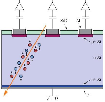
27 Measurements with Si-detectors Si-detector Si-detector with slit cover Energy loss measurement of α-particles in air detector principle Δx

 and depleted zone")

28 Surface Barrier Detectors Different Fermi energies adjust to on contact. Thin metal film on Si surface produces space charge, an effective barrier (contact potential) and depleted zone free of carriers. Apply reverse bias to increase depletion depth. Possible: depletion depth ~ 300μm dead layer d d 1μ V ~ 0.5 V/μ Over-bias reduces d d

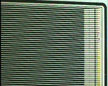
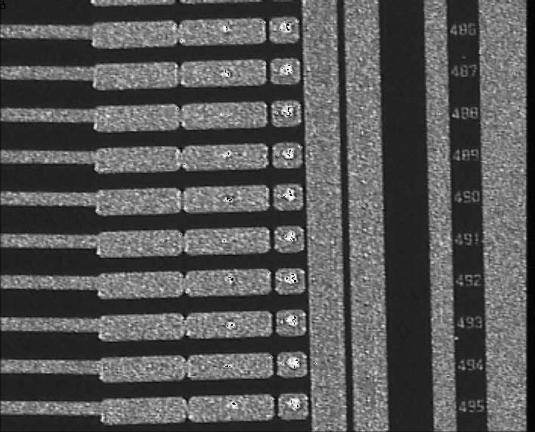
29 Principle of microstrip detector surface of a Microstrip detector bonding pads
30 Germanium detector Interaction in a Ge crystal: Photo effect (low γ-ray energy) Compton scattering (medium γ-ray energy) Pair production e + e - (high γ-ray energy) conduction band 0.7 ev 3 ev valence band Number of electron-hole pairs for 1 MeV, N = 10 6 / 3 = energy resolution = N N = kev E γ
 Pair production e + e - (high γ-ray")
31 Germanium detector Interaction in a Ge crystal: Photo effect (low γ-ray energy) Compton scattering (medium γ-ray energy) Pair production e + e - (high γ-ray energy)
 Pair production e + e - (high γ-ray energy) peak-to-total ratio unsuppressed P/T~0.15 Compton suppressed P/T~0.")
32 Compton suppressed Germanium detektor Interaction in a Ge crystal: Photo effect (low γ-ray energy) Compton scattering (medium γ-ray energy) Pair production e + e - (high γ-ray energy) peak-to-total ratio unsuppressed P/T~0.15 Compton suppressed P/T~0.6
33 Gamma-ray spectrum of a radioactive decay Pb X-ray Pb-Box BSc γ kev γ 2 DE γ 2 SE γ 2 CE γ 2 γ 1 +γ 2


34 EUROBALL (Legnaro / Strasbourg) 15 seven-fold Cluster detectors 30 coaxial detectors 26 four-fold Clover detectors


35 Making a High Purity Germanium detector Coaxial Ge detectors The hard part: Don t spoil purity of the Ge crystal (HPGe imp./cm 3 ; e.g. 1ng Cu = atoms and 10 9 Cu atoms per cm 3 already deteriorates FWHM [L. Van Goethem et al., NIM A240 (1985) 365])
Silicon Detectors in High Energy Physics
 Thomas Bergauer (HEPHY Vienna) IPM Teheran 22 May 2011 Sunday: Schedule Silicon Detectors in Semiconductor Basics (45 ) Detector concepts: Pixels and Strips (45 ) Coffee Break Strip Detector Performance
Semiconductor-Detectors
 Semiconductor-Detectors 1 Motivation ~ 195: Discovery that pn-- junctions can be used to detect particles. Semiconductor detectors used for energy measurements ( Germanium) Since ~ 3 years: Semiconductor
Chapter 1 Overview of Semiconductor Materials and Physics
 Chapter 1 Overview of Semiconductor Materials and Physics Professor Paul K. Chu Conductivity / Resistivity of Insulators, Semiconductors, and Conductors Semiconductor Elements Period II III IV V VI 2 B
Solid State Detectors Semiconductor detectors Halbleiterdetektoren
 Solid State Detectors Semiconductor detectors Halbleiterdetektoren Doris Eckstein DESY Where are solid state detectors used? > Nuclear Physics: Energy measurement of charged particles (particles up to
Lecture 2 Electrons and Holes in Semiconductors
 EE 471: Transport Phenomena in Solid State Devices Spring 2018 Lecture 2 Electrons and Holes in Semiconductors Bryan Ackland Department of Electrical and Computer Engineering Stevens Institute of Technology
Lecture 18. New gas detectors Solid state trackers
 Lecture 18 New gas detectors Solid state trackers Time projection Chamber Full 3-D track reconstruction x-y from wires and segmented cathode of MWPC z from drift time de/dx information (extra) Drift over
PN Junction
 P Junction 2017-05-04 Definition Power Electronics = semiconductor switches are used Analogue amplifier = high power loss 250 200 u x 150 100 u Udc i 50 0 0 50 100 150 200 250 300 350 400 i,u dc i,u u
Semiconductor Detectors
 Semiconductor Detectors Summary of Last Lecture Band structure in Solids: Conduction band Conduction band thermal conductivity: E g > 5 ev Valence band Insulator Charge carrier in conductor: e - Charge
Chem 481 Lecture Material 3/20/09
 Chem 481 Lecture Material 3/20/09 Radiation Detection and Measurement Semiconductor Detectors The electrons in a sample of silicon are each bound to specific silicon atoms (occupy the valence band). If
Chap. 11 Semiconductor Diodes
 Chap. 11 Semiconductor Diodes Semiconductor diodes provide the best resolution for energy measurements, silicon based devices are generally used for charged-particles, germanium for photons. Scintillators
smal band gap Saturday, April 9, 2011
 small band gap upper (conduction) band empty small gap valence band filled 2s 2p 2s 2p hybrid (s+p)band 2p no gap 2s (depend on the crystallographic orientation) extrinsic semiconductor semi-metal electron
Lecture 2. Semiconductor Physics. Sunday 4/10/2015 Semiconductor Physics 1-1
 Lecture 2 Semiconductor Physics Sunday 4/10/2015 Semiconductor Physics 1-1 Outline Intrinsic bond model: electrons and holes Charge carrier generation and recombination Intrinsic semiconductor Doping:
CLASS 12th. Semiconductors
 CLASS 12th Semiconductors 01. Distinction Between Metals, Insulators and Semi-Conductors Metals are good conductors of electricity, insulators do not conduct electricity, while the semiconductors have
Basic cell design. Si cell
 Basic cell design Si cell 1 Concepts needed to describe photovoltaic device 1. energy bands in semiconductors: from bonds to bands 2. free carriers: holes and electrons, doping 3. electron and hole current:
EE143 Fall 2016 Microfabrication Technologies. Evolution of Devices
 EE143 Fall 2016 Microfabrication Technologies Prof. Ming C. Wu wu@eecs.berkeley.edu 511 Sutardja Dai Hall (SDH) 1-1 Evolution of Devices Yesterday s Transistor (1947) Today s Transistor (2006) 1-2 1 Why
Semiconductors 1. Explain different types of semiconductors in detail with necessary bond diagrams. Intrinsic semiconductors:
 Semiconductors 1. Explain different types of semiconductors in detail with necessary bond diagrams. There are two types of semi conductors. 1. Intrinsic semiconductors 2. Extrinsic semiconductors Intrinsic
Unit IV Semiconductors Engineering Physics
 Introduction A semiconductor is a material that has a resistivity lies between that of a conductor and an insulator. The conductivity of a semiconductor material can be varied under an external electrical
CME 300 Properties of Materials. ANSWERS: Homework 9 November 26, As atoms approach each other in the solid state the quantized energy states:
 CME 300 Properties of Materials ANSWERS: Homework 9 November 26, 2011 As atoms approach each other in the solid state the quantized energy states: are split. This splitting is associated with the wave
Semiconductors. SEM and EDAX images of an integrated circuit. SEM EDAX: Si EDAX: Al. Institut für Werkstoffe der ElektrotechnikIWE
 SEM and EDAX images of an integrated circuit SEM EDAX: Si EDAX: Al source: [Cal 99 / 605] M&D-.PPT, slide: 1, 12.02.02 Classification semiconductors electronic semiconductors mixed conductors ionic conductors
EECS143 Microfabrication Technology
 EECS143 Microfabrication Technology Professor Ali Javey Introduction to Materials Lecture 1 Evolution of Devices Yesterday s Transistor (1947) Today s Transistor (2006) Why Semiconductors? Conductors e.g
Semiconductors. Semiconductors also can collect and generate photons, so they are important in optoelectronic or photonic applications.
 Semiconductors Semiconducting materials have electrical properties that fall between true conductors, (like metals) which are always highly conducting and insulators (like glass or plastic or common ceramics)
Solid State Detectors
 Solid State Detectors Most material is taken from lectures by Michael Moll/CERN and Daniela Bortoletto/Purdue and the book Semiconductor Radiation Detectors by Gerhard Lutz. In gaseous detectors, a charged
Classification of Solids
 Classification of Solids Classification by conductivity, which is related to the band structure: (Filled bands are shown dark; D(E) = Density of states) Class Electron Density Density of States D(E) Examples
Semiconductor Detectors are Ionization Chambers. Detection volume with electric field Energy deposited positive and negative charge pairs
 1 V. Semiconductor Detectors V.1. Principles Semiconductor Detectors are Ionization Chambers Detection volume with electric field Energy deposited positive and negative charge pairs Charges move in field
Introduction to Engineering Materials ENGR2000. Dr.Coates
 Introduction to Engineering Materials ENGR2000 Chapter 18: Electrical Properties Dr.Coates 18.2 Ohm s Law V = IR where R is the resistance of the material, V is the voltage and I is the current. l R A
Lecture 2. Introduction to semiconductors Structures and characteristics in semiconductors
 Lecture 2 Introduction to semiconductors Structures and characteristics in semiconductors Semiconductor p-n junction Metal Oxide Silicon structure Semiconductor contact Literature Glen F. Knoll, Radiation
Chemistry Instrumental Analysis Lecture 8. Chem 4631
 Chemistry 4631 Instrumental Analysis Lecture 8 UV to IR Components of Optical Basic components of spectroscopic instruments: stable source of radiant energy transparent container to hold sample device
Introduction to Semiconductor Physics. Prof.P. Ravindran, Department of Physics, Central University of Tamil Nadu, India
 Introduction to Semiconductor Physics 1 Prof.P. Ravindran, Department of Physics, Central University of Tamil Nadu, India http://folk.uio.no/ravi/cmp2013 Review of Semiconductor Physics Semiconductor fundamentals
Lecture 1. OUTLINE Basic Semiconductor Physics. Reading: Chapter 2.1. Semiconductors Intrinsic (undoped) silicon Doping Carrier concentrations
 silicon Doping Carrier concentrations") Lecture 1 OUTLINE Basic Semiconductor Physics Semiconductors Intrinsic (undoped) silicon Doping Carrier concentrations Reading: Chapter 2.1 EE105 Fall 2007 Lecture 1, Slide 1 What is a Semiconductor? Low
Lecture 1 OUTLINE Basic Semiconductor Physics Semiconductors Intrinsic (undoped) silicon Doping Carrier concentrations Reading: Chapter 2.1 EE105 Fall 2007 Lecture 1, Slide 1 What is a Semiconductor? Low
Radiation Detector 2016/17 (SPA6309)
") Radiation Detector 2016/17 (SPA6309) Semiconductor detectors (Leo, Chapter 10) 2017 Teppei Katori Semiconductor detectors are used in many situations, mostly for some kind of high precision measurement.
Radiation Detector 2016/17 (SPA6309) Semiconductor detectors (Leo, Chapter 10) 2017 Teppei Katori Semiconductor detectors are used in many situations, mostly for some kind of high precision measurement.
EECS130 Integrated Circuit Devices
 EECS130 Integrated Circuit Devices Professor Ali Javey 8/30/2007 Semiconductor Fundamentals Lecture 2 Read: Chapters 1 and 2 Last Lecture: Energy Band Diagram Conduction band E c E g Band gap E v Valence
ESE 372 / Spring 2013 / Lecture 5 Metal Oxide Semiconductor Field Effect Transistor
 Metal Oxide Semiconductor Field Effect Transistor V G V G 1 Metal Oxide Semiconductor Field Effect Transistor We will need to understand how this current flows through Si What is electric current? 2 Back
Electro - Principles I
 Electro - Principles I Page 10-1 Atomic Theory It is necessary to know what goes on at the atomic level of a semiconductor so the characteristics of the semiconductor can be understood. In many cases a
Engineering 2000 Chapter 8 Semiconductors. ENG2000: R.I. Hornsey Semi: 1
 Engineering 2000 Chapter 8 Semiconductors ENG2000: R.I. Hornsey Semi: 1 Overview We need to know the electrical properties of Si To do this, we must also draw on some of the physical properties and we
ELECTRONIC DEVICES AND CIRCUITS SUMMARY
 ELECTRONIC DEVICES AND CIRCUITS SUMMARY Classification of Materials: Insulator: An insulator is a material that offers a very low level (or negligible) of conductivity when voltage is applied. Eg: Paper,
Charge Carriers in Semiconductor
 Charge Carriers in Semiconductor To understand PN junction s IV characteristics, it is important to understand charge carriers behavior in solids, how to modify carrier densities, and different mechanisms
Ga and P Atoms to Covalent Solid GaP
 Ga and P Atoms to Covalent Solid GaP Band Gaps in Binary Group III-V Semiconductors Mixed Semiconductors Affect of replacing some of the As with P in GaAs Band Gap (ev) (nm) GaAs 1.35 919 (IR) GaP 2.24
electronics fundamentals
 electronics fundamentals circuits, devices, and applications THOMAS L. FLOYD DAVID M. BUCHLA Lesson 1: Diodes and Applications Semiconductors Figure 1-1 The Bohr model of an atom showing electrons in orbits
A semiconductor is an almost insulating material, in which by contamination (doping) positive or negative charge carriers can be introduced.
 positive or negative charge carriers can be introduced.") Semiconductor A semiconductor is an almost insulating material, in which by contamination (doping) positive or negative charge carriers can be introduced. Page 2 Semiconductor materials Page 3 Energy levels
Semiconductor A semiconductor is an almost insulating material, in which by contamination (doping) positive or negative charge carriers can be introduced. Page 2 Semiconductor materials Page 3 Energy levels
Semiconductor X-Ray Detectors. Tobias Eggert Ketek GmbH
 Semiconductor X-Ray Detectors Tobias Eggert Ketek GmbH Semiconductor X-Ray Detectors Part A Principles of Semiconductor Detectors 1. Basic Principles 2. Typical Applications 3. Planar Technology 4. Read-out
Crystal Properties. MS415 Lec. 2. High performance, high current. ZnO. GaN
 Crystal Properties Crystal Lattices: Periodic arrangement of atoms Repeated unit cells (solid-state) Stuffing atoms into unit cells Determine mechanical & electrical properties High performance, high current
Electron Energy, E E = 0. Free electron. 3s Band 2p Band Overlapping energy bands. 3p 3s 2p 2s. 2s Band. Electrons. 1s ATOM SOLID.
 Electron Energy, E Free electron Vacuum level 3p 3s 2p 2s 2s Band 3s Band 2p Band Overlapping energy bands Electrons E = 0 1s ATOM 1s SOLID In a metal the various energy bands overlap to give a single
n N D n p = n i p N A
 Summary of electron and hole concentration in semiconductors Intrinsic semiconductor: E G n kt i = pi = N e 2 0 Donor-doped semiconductor: n N D where N D is the concentration of donor impurity Acceptor-doped
Lecture (02) Introduction to Electronics II, PN Junction and Diodes I
 Introduction to Electronics II, PN Junction and Diodes I") Lecture (02) Introduction to Electronics II, PN Junction and Diodes I By: Dr. Ahmed ElShafee ١ Agenda Current in semiconductors/conductors N type, P type semiconductors N Type Semiconductor P Type Semiconductor
Lecture (02) Introduction to Electronics II, PN Junction and Diodes I By: Dr. Ahmed ElShafee ١ Agenda Current in semiconductors/conductors N type, P type semiconductors N Type Semiconductor P Type Semiconductor
LN 3 IDLE MIND SOLUTIONS
 IDLE MIND SOLUTIONS 1. Let us first look in most general terms at the optical properties of solids with band gaps (E g ) of less than 4 ev, semiconductors by definition. The band gap energy (E g ) can
* motif: a single or repeated design or color
 Chapter 2. Structure A. Electronic structure vs. Geometric structure B. Clean surface vs. Adsorbate covered surface (substrate + overlayer) C. Adsorbate structure - how are the adsorbed molecules bound
Lecture 2. Introduction to semiconductors Structures and characteristics in semiconductors
 Lecture 2 Introduction to semiconductors Structures and characteristics in semiconductors Semiconductor p-n junction Metal Oxide Silicon structure Semiconductor contact Literature Glen F. Knoll, Radiation
EE301 Electronics I , Fall
 EE301 Electronics I 2018-2019, Fall 1. Introduction to Microelectronics (1 Week/3 Hrs.) Introduction, Historical Background, Basic Consepts 2. Rewiev of Semiconductors (1 Week/3 Hrs.) Semiconductor materials
Introductory Nanotechnology ~ Basic Condensed Matter Physics ~
 Introductory Nanotechnology ~ Basic Condensed Matter Physics ~ Atsufumi Hirohata Department of Electronics Quick Review over the Last Lecture Classic model : Dulong-Petit empirical law c V, mol 3R 0 E
Semiconductor physics I. The Crystal Structure of Solids
 Lecture 3 Semiconductor physics I The Crystal Structure of Solids 1 Semiconductor materials Types of solids Space lattices Atomic Bonding Imperfection and doping in SOLIDS 2 Semiconductor Semiconductors
Lecture 3 Transport in Semiconductors
 EE 471: Transport Phenomena in Solid State Devices Spring 2018 Lecture 3 Transport in Semiconductors Bryan Ackland Department of Electrical and Computer Engineering Stevens Institute of Technology Hoboken,
Gamma and X-Ray Detection
 Gamma and X-Ray Detection DETECTOR OVERVIEW The kinds of detectors commonly used can be categorized as: a. Gas-filled Detectors b. Scintillation Detectors c. Semiconductor Detectors The choice of a particular
KATIHAL FİZİĞİ MNT-510
 KATIHAL FİZİĞİ MNT-510 YARIİLETKENLER Kaynaklar: Katıhal Fiziği, Prof. Dr. Mustafa Dikici, Seçkin Yayıncılık Katıhal Fiziği, Şakir Aydoğan, Nobel Yayıncılık, Physics for Computer Science Students: With
SEMICONDUCTOR PHYSICS
 SEMICONDUCTOR PHYSICS by Dibyendu Chowdhury Semiconductors The materials whose electrical conductivity lies between those of conductors and insulators, are known as semiconductors. Silicon Germanium Cadmium
3.1 Introduction to Semiconductors. Y. Baghzouz ECE Department UNLV
 3.1 Introduction to Semiconductors Y. Baghzouz ECE Department UNLV Introduction In this lecture, we will cover the basic aspects of semiconductor materials, and the physical mechanisms which are at the
Diodes. EE223 Digital & Analogue Electronics Derek Molloy 2012/2013.
 Diodes EE223 Digital & Analogue Electronics Derek Molloy 2012/2013 Derek.Molloy@dcu.ie Diodes: A Semiconductor? Conductors Such as copper, aluminium have a cloud of free electrons weak bound valence electrons
Energetic particles and their detection in situ (particle detectors) Part II. George Gloeckler
 Part II. George Gloeckler") Energetic particles and their detection in situ (particle detectors) Part II George Gloeckler University of Michigan, Ann Arbor, MI University of Maryland, College Park, MD Simple particle detectors Gas-filled
Energetic particles and their detection in situ (particle detectors) Part II George Gloeckler University of Michigan, Ann Arbor, MI University of Maryland, College Park, MD Simple particle detectors Gas-filled
ECE 335: Electronic Engineering Lecture 2: Semiconductors
 Faculty of Engineering ECE 335: Electronic Engineering Lecture 2: Semiconductors Agenda Intrinsic Semiconductors Extrinsic Semiconductors N-type P-type Carrier Transport Drift Diffusion Semiconductors
12/10/09. Chapter 18: Electrical Properties. View of an Integrated Circuit. Electrical Conduction ISSUES TO ADDRESS...
 Chapter 18: Electrical Properties ISSUES TO ADDRESS... How are electrical conductance and resistance characterized? What are the physical phenomena that distinguish? For metals, how is affected by and
Electronics The basics of semiconductor physics
 Electronics The basics of semiconductor physics Prof. Márta Rencz, Gergely Nagy BME DED September 16, 2013 The basic properties of semiconductors Semiconductors conductance is between that of conductors
Electronic Circuits for Mechatronics ELCT 609 Lecture 2: PN Junctions (1)
") Electronic Circuits for Mechatronics ELCT 609 Lecture 2: PN Junctions (1) Assistant Professor Office: C3.315 E-mail: eman.azab@guc.edu.eg 1 Electronic (Semiconductor) Devices P-N Junctions (Diodes): Physical
Electronic Circuits for Mechatronics ELCT 609 Lecture 2: PN Junctions (1) Assistant Professor Office: C3.315 E-mail: eman.azab@guc.edu.eg 1 Electronic (Semiconductor) Devices P-N Junctions (Diodes): Physical
Electronic PRINCIPLES
 MALVINO & BATES Electronic PRINCIPLES SEVENTH EDITION Chapter 2 Semiconductors Topics Covered in Chapter 2 Conductors Semiconductors Silicon crystals Intrinsic semiconductors Two types of flow Doping a
EE495/695 Introduction to Semiconductors I. Y. Baghzouz ECE Department UNLV
 EE495/695 Introduction to Semiconductors I Y. Baghzouz ECE Department UNLV Introduction Solar cells have always been aligned closely with other electronic devices. We will cover the basic aspects of semiconductor
Components of a generic collider detector
 Lecture 24 Components of a generic collider detector electrons - ionization + bremsstrahlung photons - pair production in high Z material charged hadrons - ionization + shower of secondary interactions
EE 446/646 Photovoltaic Devices I. Y. Baghzouz
 EE 446/646 Photovoltaic Devices I Y. Baghzouz What is Photovoltaics? First used in about 1890, the word has two parts: photo, derived from the Greek word for light, volt, relating to electricity pioneer
LEC E T C U T R U E R E 17 -Photodetectors
 LECTURE 17 -Photodetectors Topics to be covered Photodetectors PIN photodiode Avalanche Photodiode Photodetectors Principle of the p-n junction Photodiode A generic photodiode. Photodetectors Principle
Introduction to Transistors. Semiconductors Diodes Transistors
 Introduction to Transistors Semiconductors Diodes Transistors 1 Semiconductors Typical semiconductors, like silicon and germanium, have four valence electrons which form atomic bonds with neighboring atoms
EE 5344 Introduction to MEMS CHAPTER 5 Radiation Sensors
 EE 5344 Introduction to MEMS CHAPTER 5 Radiation Sensors 5. Radiation Microsensors Radiation µ-sensors convert incident radiant signals into standard electrical out put signals. Radiant Signals Classification
ISSUES TO ADDRESS...
 Chapter 12: Electrical Properties School of Mechanical Engineering Choi, Hae-Jin Materials Science - Prof. Choi, Hae-Jin Chapter 12-1 ISSUES TO ADDRESS... How are electrical conductance and resistance
Atoms? All matters on earth made of atoms (made up of elements or combination of elements).
.") Chapter 1 Atoms? All matters on earth made of atoms (made up of elements or combination of elements). Atomic Structure Atom is the smallest particle of an element that can exist in a stable or independent
Chapter 1 Atoms? All matters on earth made of atoms (made up of elements or combination of elements). Atomic Structure Atom is the smallest particle of an element that can exist in a stable or independent
Minimal Update of Solid State Physics
 Minimal Update of Solid State Physics It is expected that participants are acquainted with basics of solid state physics. Therefore here we will refresh only those aspects, which are absolutely necessary
ECE 250 Electronic Devices 1. Electronic Device Modeling
 ECE 250 Electronic Devices 1 ECE 250 Electronic Device Modeling ECE 250 Electronic Devices 2 Introduction to Semiconductor Physics You should really take a semiconductor device physics course. We can only
Semiconductor Detectors
 Radiation Measurement Systems Semiconductor Detectors Ho Kyung Kim Pusan National University Semiconductors Differences btwn semiconductor & gas as a material for radiation detectors Higher (1,000 ) Free
Solid State Physics SEMICONDUCTORS - IV. Lecture 25. A.H. Harker. Physics and Astronomy UCL
 Solid State Physics SEMICONDUCTORS - IV Lecture 25 A.H. Harker Physics and Astronomy UCL 9.9 Carrier diffusion and recombination Suppose we have a p-type semiconductor, i.e. n h >> n e. (1) Create a local
Review of Semiconductor Fundamentals
 ECE 541/ME 541 Microelectronic Fabrication Techniques Review of Semiconductor Fundamentals Zheng Yang (ERF 3017, email: yangzhen@uic.edu) Page 1 Semiconductor A semiconductor is an almost insulating material,
Semiconductor Devices and Circuits Fall Midterm Exam. Instructor: Dr. Dietmar Knipp, Professor of Electrical Engineering. Name: Mat. -Nr.
 Semiconductor Devices and Circuits Fall 2003 Midterm Exam Instructor: Dr. Dietmar Knipp, Professor of Electrical Engineering Name: Mat. -Nr.: Guidelines: Duration of the Midterm: 1 hour The exam is a closed
1 Name: Student number: DEPARTMENT OF PHYSICS AND PHYSICAL OCEANOGRAPHY MEMORIAL UNIVERSITY OF NEWFOUNDLAND. Fall :00-11:00
 1 Name: DEPARTMENT OF PHYSICS AND PHYSICAL OCEANOGRAPHY MEMORIAL UNIVERSITY OF NEWFOUNDLAND Final Exam Physics 3000 December 11, 2012 Fall 2012 9:00-11:00 INSTRUCTIONS: 1. Answer all seven (7) questions.
Course overview. Me: Dr Luke Wilson. The course: Physics and applications of semiconductors. Office: E17 open door policy
 Course overview Me: Dr Luke Wilson Office: E17 open door policy email: luke.wilson@sheffield.ac.uk The course: Physics and applications of semiconductors 10 lectures aim is to allow time for at least one
Conductivity and Semi-Conductors
 Conductivity and Semi-Conductors J = current density = I/A E = Electric field intensity = V/l where l is the distance between two points Metals: Semiconductors: Many Polymers and Glasses 1 Electrical Conduction
Lecture 2. Introduction to semiconductors Structures and characteristics in semiconductors. Fabrication of semiconductor sensor
 Lecture 2 Introduction to semiconductors Structures and characteristics in semiconductors Semiconductor p-n junction Metal Oxide Silicon structure Semiconductor contact Fabrication of semiconductor sensor
Solid State Device Fundamentals
 Solid State Device Fundamentals ENS 345 Lecture Course by Alexander M. Zaitsev alexander.zaitsev@csi.cuny.edu Tel: 718 982 2812 Office 4N101b 1 The free electron model of metals The free electron model
p-n junction biasing, p-n I-V characteristics, p-n currents Norlaili Mohd. Noh EEE /09
 CLASS 6&7 p-n junction biasing, p-n I-V characteristics, p-n currents 1 p-n junction biasing Unbiased p-n junction: the potential barrier is 0.7 V for Si and 0.3 V for Ge. Nett current across the p-n junction
Lecture (02) PN Junctions and Diodes
 PN Junctions and Diodes") Lecture (02) PN Junctions and Diodes By: Dr. Ahmed ElShafee ١ I Agenda N type, P type semiconductors N Type Semiconductor P Type Semiconductor PN junction Energy Diagrams of the PN Junction and Depletion
Lecture (02) PN Junctions and Diodes By: Dr. Ahmed ElShafee ١ I Agenda N type, P type semiconductors N Type Semiconductor P Type Semiconductor PN junction Energy Diagrams of the PN Junction and Depletion
DETECTORS. I. Charged Particle Detectors
 DETECTORS I. Charged Particle Detectors A. Scintillators B. Gas Detectors 1. Ionization Chambers 2. Proportional Counters 3. Avalanche detectors 4. Geiger-Muller counters 5. Spark detectors C. Solid State
Chapter 1 Semiconductor basics
 Chapter 1 Semiconductor basics ELEC-H402/CH1: Semiconductor basics 1 Basic semiconductor concepts Semiconductor basics Semiconductors, silicon and hole-electron pair Intrinsic silicon properties Doped
Electrical Properties
 Electrical Properties Electrical Conduction R Ohm s law V = IR I l Area, A V where I is current (Ampere), V is voltage (Volts) and R is the resistance (Ohms or ) of the conductor Resistivity Resistivity,
collisions of electrons. In semiconductor, in certain temperature ranges the conductivity increases rapidly by increasing temperature
 1.9. Temperature Dependence of Semiconductor Conductivity Such dependence is one most important in semiconductor. In metals, Conductivity decreases by increasing temperature due to greater frequency of
The photovoltaic effect occurs in semiconductors where there are distinct valence and
 How a Photovoltaic Cell Works The photovoltaic effect occurs in semiconductors where there are distinct valence and conduction bands. (There are energies at which electrons can not exist within the solid)
Lecture 9: Metal-semiconductor junctions
 Lecture 9: Metal-semiconductor junctions Contents 1 Introduction 1 2 Metal-metal junction 1 2.1 Thermocouples.......................... 2 3 Schottky junctions 4 3.1 Forward bias............................
Chapter 4: Bonding in Solids and Electronic Properties. Free electron theory
 Chapter 4: Bonding in Solids and Electronic Properties Free electron theory Consider free electrons in a metal an electron gas. regards a metal as a box in which electrons are free to move. assumes nuclei
Semiconductor Physics and Devices
 The pn Junction 1) Charge carriers crossing the junction. 3) Barrier potential Semiconductor Physics and Devices Chapter 8. The pn Junction Diode 2) Formation of positive and negative ions. 4) Formation
Section 12: Intro to Devices
 Section 12: Intro to Devices Extensive reading materials on reserve, including Robert F. Pierret, Semiconductor Device Fundamentals Bond Model of Electrons and Holes Si Si Si Si Si Si Si Si Si Silicon
Ch. 2: Energy Bands And Charge Carriers In Semiconductors
 Ch. 2: Energy Bands And Charge Carriers In Semiconductors Discrete energy levels arise from balance of attraction force between electrons and nucleus and repulsion force between electrons each electron
Lecture 7: Extrinsic semiconductors - Fermi level
 Lecture 7: Extrinsic semiconductors - Fermi level Contents 1 Dopant materials 1 2 E F in extrinsic semiconductors 5 3 Temperature dependence of carrier concentration 6 3.1 Low temperature regime (T < T
Charge carrier density in metals and semiconductors
 Charge carrier density in metals and semiconductors 1. Introduction The Hall Effect Particles must overlap for the permutation symmetry to be relevant. We saw examples of this in the exchange energy in
ELEC 4700 Assignment #2
 ELEC 4700 Assignment #2 Question 1 (Kasop 4.2) Molecular Orbitals and Atomic Orbitals Consider a linear chain of four identical atoms representing a hypothetical molecule. Suppose that each atomic wavefunction
EE 346: Semiconductor Devices
 EE 346: Semiconductor Devices Lecture - 6 02/06/2017 Tewodros A. Zewde 1 DENSTY OF STATES FUNCTON Since current is due to the flow of charge, an important step in the process is to determine the number
Semiconductors and Optoelectronics. Today Semiconductors Acoustics. Tomorrow Come to CH325 Exercises Tours
 Semiconductors and Optoelectronics Advanced Physics Lab, PHYS 3600 Don Heiman, Northeastern University, 2017 Today Semiconductors Acoustics Tomorrow Come to CH325 Exercises Tours Semiconductors and Optoelectronics
ELECTRONIC I Lecture 1 Introduction to semiconductor. By Asst. Prof Dr. Jassim K. Hmood
 ELECTRONIC I Lecture 1 Introduction to semiconductor By Asst. Prof Dr. Jassim K. Hmood SOLID-STATE ELECTRONIC MATERIALS Electronic materials generally can be divided into three categories: insulators,
Semiconductor Physics fall 2012 problems
 Semiconductor Physics fall 2012 problems 1. An n-type sample of silicon has a uniform density N D = 10 16 atoms cm -3 of arsenic, and a p-type silicon sample has N A = 10 15 atoms cm -3 of boron. For each