Tracking in High Energy Physics: Silicon Devices!
|
|
|
- Paula Ward
- 6 years ago
- Views:
Transcription

1 Tracking in High Energy Physics: Silicon Devices! G. Leibenguth XIX Graduiertenkolleg Heidelberg October 2007
2 Content Part 1: Basics on semi-conductor Part 2: Construction Part 3: Two Examples Part 4: Future (radiation, 3d processing, )
3 Disclaimer and Reference Do not expect to have a solid state physics lecture Reference: R. Horisberger, talk given at the conference vertex 2006 C. Delaere, talk given at the conference vertex 2007 A. Homna, lecture given at the NATO advanced study (2002) And material taken from colleagues from CMS, ATLAS and other
4 Outline of the Lectures Today Lecture 1 A bit of history Motivation Silicon strip detector (principle) Performance required Lecture 2 Fabrication of sensors Constructions of detector modules Readout electronics
5 A bit of history First use of silicon detectors in HEP experiments: the 50 s: energy measurement Precision measurement up until 70 s: Emulsion or bubble chambers => Limited rate and no triggering Traditional gas detectors (limited to a spatial resolution of µm) First usage (late 70 s) precision measurement (lifetime): Secondary vertex tagging (charm, in fixed target) Segment sensors (strips) with pitch First silicon pixel devices (NA32) charm experiment
6 Why wasn t it used before? First Reason: Excessive material (electronics) in active volume Advance in electronics miniaturization and low composite structures Late 80 s, early 90 s: Mark II (SLC) and all 4 LEP experiments Use of Silicon limited to small region near interaction point: both silicon and electronics were very expensive
7 Motivation Charged particle position measurement: Ionization signal (de/dx) left by a charged particle crossing the detector _ + -_ - Use the drift chamber analogy (see C. Niebuhr s lecture) where ionization produces electron-ion pairs, and an electric field is applied to collect electrons and ions to the opposite charged electrode In a semi-conductor, pair of electron-holes are produced with 3.6 ev. Quickly recombine. How are the charges drifting?
8 Collected charge From the Bethe-Bloch s formula (see C. Niebuhr lecture), One can calculate the minimum ionization deposition: de/dx Si = 3.88 MeV/cm. For 300 µm thickness, 116 kev Most probable loss (0.7*mean) => 81 kev 3.6 ev to make an e-h pair Max collected charge: e (=3.6 fc)
9 Solid states physics What does one need to know from the principle to design, build and operate a silicon detector: Property of material Energy bands Junction PN
10 Property of Material

11 Semi-conductor Silicon, Germanium, Diamond GaAs?
12 Semi-conductor: Silicon Most important semi-conductor for detector development Is silicon (even so Germanium is used for calorimetry, Thanks to an excellent energy resolution) Silicon makes up to 25.7 % of earth s crust by weight, and the second most abundant element, being exceed only by Oxygen. Silicon is not found free in nature, but appears as oxide and as silicates: 1) Sand, quartz, rock crystal,amethyst, agate, flint 2) Granite hornblende, asbestos, feldspar, clay, mica, etc
13 More details on Silicon Atomic Number (A): 28 Charge: 14 Melting Point: 1687 K Atomic Symbol: Si Boiling Point: 3538 K Atomic Weight: Density: g/cm 3 Electronic Configuration: (Ne) (3s) 2 (3p) 2 Ionization Potential: 8.1eV 4 Valence electrons

14 Reminder: Crystallography Simple body centered Face

15 Body centered cubic structure The body centered cubic structure shown a two interlinked simple cubic structure Many metals own this structure, like iron, lithium, potassium, etc
 and a photograph of a Si 111")
16 Miller Indices, Si (111) Silicon (111) plane (solid line) and a photograph of a Si 111 surface
17 Valence Bond Miller Indices, Si (111) The silicon crystal is bound via valence bonds 4 valence electrons: Silicon is tetravalent Each electron can be only associated with: Positive ion cores should be kept apart to minimize the coulomb energy Valence electrons should also be kept apart Valence electrons should stay close to positive ions to maximize attraction

18 Energy band Reminder: free electron! k = 2 h 2m k r 2 Plot of energy versus wave vector k for a free electron and for an electron in a mono-atomic linear lattice (constant a)

19 Conduction band The probability that an electron occupies an Energy level is given by the Fermi-Dirac Distribution: For N e = N h E f = E gap /2
20 Intrinsic semi-conductors
21 Acceptors and donors If the semiconductor is doped then impurity energy levels are introduced For example, if a boron atom replaces a Si atom then as the boron owns only three valence electrons, a hole is created in the crystal. Using an atom of arsenic donate a electron to the conduction band, making it more N (negative) type
22 Extrinsic semi-conductor One can dramatically change the conductivity property of a semi-conductor by adding impurities: more electrons or more holes (we speak of extrinsicness ) Add to molten valence 4 atom with valence 3 or valence 5 during crystallization High speed injection of such kind of atoms Net result: extra allowed energy level in the forbidden band gap, electron can jump from the valence band (p-type doping)

23 N-type N = N d Fermi level becomes: E c - E f = kt ln(n c /N d ) Number of donors is increased while the Fermi energy move toward the conduction band

24 P-type P-type is an acceptor: Replacing some silicon atom by boron: The Fermi energy moves also toward the conduction band
25 P-type viewed from eg Level

26 Signal formation in silicon At t=0 o K, conduction band empty Distribution according to Fermi- Dirac statistics Number of electrons in the conduction band a temperature T: Implies: Ratio of electrons in the conduction band is 10-12

27 A MIP in a silicon slice A volume of 1cm x 1cm x 300 µm contains about 4.5 x 10 8 free charge carriers compared to only electron-hole pair for a MIP at room temperature Number of free charge carriers is way too much Solution: Cooling PN Junction
28 PN-junction Exploit the properties of a p-n junction to collect the ionization charges: When brought together appear a gradient of electron and hole densities resulting in a diffusive migration of majority carriers across the junction.

29 PN-junction The migration leaves a region of net opposite charges: the space charge region Electric Field prevent move of charge carrier e-h pairs will not recombine, but drift away

30 PN-junction, depletion region Make the junction p-n at a surface of a silicon wafer with the n-type bulk, extend the depletion zone throughout to get the maximum charge collection To get it, apply a reverse bias voltage (why reverse => direct results in a current flow)
 Higher voltage for low resistivity material Higher voltage also needed for a p-type bulk (carrier mobility of holes lower")
31 Property of the depletion zone Depletion width depends on the resistivity, charge carrier and magnitude of bias voltage V b w = (2ερµV b ) Bias Voltage needed to completely deplete a device of thickness d is called the depletion voltage Two remarks: V d = d 2 / (2ερµ) Higher voltage for low resistivity material Higher voltage also needed for a p-type bulk (carrier mobility of holes lower than electrons µ(mobility) ρ=1/qµn, N number of doping concentration
32 Property of the depletion zone Capacitance is simply the parallel plate capacity of the depletion zone Depletion behavior is obtained by measuring the capacitance versus reverse bias voltage: C = A ( ε / 2ρµV b )
33 Charge collected & diffusion Drift velocity of charged carriers v = µe, so drift time is: t d = d/v = d/µe Typical value d=300µm, E=2.5 kv/cm, µ e =1350 cm 2 /V.s, µ h=450 cm 2 /V.s, so t d (e)=9ns, t d (h)=27ns Diffusion of charged cloud caused by scattering of drifting charge carrier, radius of distribution after time t d R= 2Dtd) where D= µkt/q
34 Leakage currents Two main sources of current flow in reversed biased diode: Diffusion current, charge generated in the undepleted zone close to the depletion which diffuse into it. Should be negligible in a fully depleted device Generation current J g,charge generated in the depletion zone by defect or contaminants J exp(-b/kt) (Exponential dependence on temperature) Rate is determined by nature and concentrations of defects => Major Contribution!!!
 Guard rind structure")
 Defect or oxide charge build-up might increase the leakage")
35 Surface and edge effect a) Voltage drop between ring and edge b) Typical n-type implants put around edge c) Guard rind structure (floating) to improve continuous potential drop over this region d) Defect or oxide charge build-up might increase the leakage current

36 Breakdown If V bias large, field might be high enough to initiate avalanche multiplication, ie charge carriers have enough energy to produce more e-h pairs. Occurs around 30V/µm. Local defect can result in field reaching the breakdown point 1 na
37 Current in diode For a 300 µm thick sensor, about e/h pairs are created on the passage of a MIP. With a collection time of approximately 2 ns the peak current generated due to the charge deposition is approximately given by I ~ 24, 000" 1.6" 10 2" 10! 9! 19
38 DC coupled strips Diode is not very useful for high resolution: The assembly of many individual, tiny diodes, to form a large area tracking device would be both a laborious and expensive task. Each diode would also possess dead areas around the edge of the silicon leading to excess material, the need to overall and excessively complicated mounting assemblies Segmentation of the readout Strip geometry
39 Geometry: consideration does the pattern match the needs of the experiment? is this pattern consistent with the properties of silicon e.g. compatible with diffusions distances Will the segmentation yield a useful signal to noise and (closely linked) an adequate spatial resolution? (remember, we would like to measure lifetime down to picosecond)
40 DC readout Example: The H1 central silicon tracker Problem: reversed current (also known as Dark current)
41 Charge collection 1) Need to isolate strips from each other 2) Collect (measure) the charge on each strip High impedance bias, directly integrated on the sensor Issue: Strip defects Noisy strips: usually high DC leakage current Short between strips and strip to other structures Opens: Interruption of strip or no contact between metal and implants
42 AC coupled strips The AC coupled detector is designed to Overcome a major obstacle of the DC devices, that of the dark current in the diode: overtax the amplifier => saturation Reduce the dynamic range Noise on the current might mask the small high frequency signals from the particle we want to detect => Capacitive coupling to the readout electronic, which induces a charge qc on the input of the amplifier
43 Double sided detector If the strips on opposite sides of the sensor are placed at right angles to each other a space point (rather than a single coordinate) will be produced for the hit. Double sided detectors are very useful but complex and expensive to make and readout. It is often easier to use two single sided sensors in close proximity to achieve the same effect. => See the discussion later
44 Performance Resolution: strip pitch and readout pitch Capacitive charge division Signal to noise ratio Noise Radiation damage
45 Position resolution Strip and readout pitch: Assume that the detected charge is treated in a binary way, the resolution is simply: σ = p/ 12, so for a pitch of 50 µm, get 7.2 µm If the charge distribution is shared among adjacent strips, (usually the case), one can calculate the centre gravity of the charge deposit, leading to resolution below 10 µm Test devices have achieved a resolution of about 3 µm (using a readout pitch of 25 µm) which is near the limit on precision determined by diffusion and stat fluctuation of the ionizing energy deposition
46 Capacitive charge division Can we afford to read out all strips? When not Read out only every n th strip while preserving the signal magnitude. A good estimate of the centroid resolution is still obtained However, the signal to noise ration becomes very crucial

47 Signal to noise ratio (S/N) Landau distribution has a long low energy tail Becomes even lower with addition of noise
48 Main source of noise Capacitive load (C d ) dependence (ENC C d Sensor leakage current (shot noise) Parallel resistance of bias resistor (thermal noise) (kt/r) Noise generally expressed in the form: ENC = a + b. C d Noise is very frequency dependent (readout method) Implication on detector design: Strip length, device quality, choice of bias method Temperature important for both leakage and bias resistor component
49 Signal and noise Basic signal produced is around ~ electrons Typical losses of 5 to 10% due to the chosen electrical network (AC coupling capacitor, stray capacitances and resistances) and to the front-end electronics Noise: Usually expressed in term of equivalent noise charge (ENC) in unit of electron charge. The source of noise depends largely on the electronic Front-end
 Damage clusters (nuclear reaction) Non-ionizing energy loss (NIEL)")
50 Radiation damage Impact of radiation on silicon: Silicon atoms can be displaced from their lattice position: Point defects (electromagnetic radiation) Damage clusters (nuclear reaction) Non-ionizing energy loss (NIEL)
51 energy level in the band gap Direct excitation possible Higher leakage current => (more noise) Charge trapping (lower charge collection) Efficiency Higher bias voltage mandatory
52 Non ionizing energy loss Main damage for silicon strip devices is lattice displacement damage of silicon atoms (atomic displacement via nuclear interactions) For EM radiation need E>250 kev, produced point defect For neutron and charged hadrons, damage start at low energy Important: Damage creates large numbers of new donor And acceptor states: 1) Change of charge density in depletion region 2) more generation -recombination center => larger I leak
53 Effects After irradiation, the observed damage looks reduced. The rate of this is Highly temperature dependent. Annealing is partly due to true Annealing (repair of lattice defects, faster at higher temperature) But for N eff two annealing effect: Beneficial (short time scale) Reverse, cause damage to increase
54 Effect on the depletion zone N-type silicon become increasing p-type until the substrate Undergoes type inversion Voltage for a p + -n silicon device is: V dep α 1/ρ α 1/ N eff (N efi is the effective Doping concentration)
55 Effects on Leakage current: ΔI leak = αφ, α is known as the damage constant and φ is the fluence. No reverse annealing effect Thermal runaway: irradiated device heating up! Dangerous, since leakage currrent srrongly depends on temperature Charge collection: Increase of trapping states in the depletion region (10% loss of signal for φ = 2 x n/cm 2 )
56 Summary Silicon property: band gap 1.6 ev A mip passing through the detector leaves electrons-holes pairs With a bias reversed PN junction, ability to measure this charge (3.6 fc) Signal over Noise is a crucial quantity Radiation hard devices needed we will discuss the different steps of the construction of a silicon detector
Semiconductor Detectors
 Semiconductor Detectors Summary of Last Lecture Band structure in Solids: Conduction band Conduction band thermal conductivity: E g > 5 ev Valence band Insulator Charge carrier in conductor: e - Charge
Semiconductor-Detectors
 Semiconductor-Detectors 1 Motivation ~ 195: Discovery that pn-- junctions can be used to detect particles. Semiconductor detectors used for energy measurements ( Germanium) Since ~ 3 years: Semiconductor
Silicon Detectors in High Energy Physics
 Thomas Bergauer (HEPHY Vienna) IPM Teheran 22 May 2011 Sunday: Schedule Silicon Detectors in Semiconductor Basics (45 ) Detector concepts: Pixels and Strips (45 ) Coffee Break Strip Detector Performance
Solid State Detectors
 Solid State Detectors Most material is taken from lectures by Michael Moll/CERN and Daniela Bortoletto/Purdue and the book Semiconductor Radiation Detectors by Gerhard Lutz. In gaseous detectors, a charged
Energetic particles and their detection in situ (particle detectors) Part II. George Gloeckler
 Part II. George Gloeckler") Energetic particles and their detection in situ (particle detectors) Part II George Gloeckler University of Michigan, Ann Arbor, MI University of Maryland, College Park, MD Simple particle detectors Gas-filled
Energetic particles and their detection in situ (particle detectors) Part II George Gloeckler University of Michigan, Ann Arbor, MI University of Maryland, College Park, MD Simple particle detectors Gas-filled
Lecture 2. Introduction to semiconductors Structures and characteristics in semiconductors
 Lecture 2 Introduction to semiconductors Structures and characteristics in semiconductors Semiconductor p-n junction Metal Oxide Silicon structure Semiconductor contact Literature Glen F. Knoll, Radiation
Lecture 2. Introduction to semiconductors Structures and characteristics in semiconductors
 Lecture 2 Introduction to semiconductors Structures and characteristics in semiconductors Semiconductor p-n junction Metal Oxide Silicon structure Semiconductor contact Literature Glen F. Knoll, Radiation
Review of Semiconductor Fundamentals
 ECE 541/ME 541 Microelectronic Fabrication Techniques Review of Semiconductor Fundamentals Zheng Yang (ERF 3017, email: yangzhen@uic.edu) Page 1 Semiconductor A semiconductor is an almost insulating material,
Advantages / Disadvantages of semiconductor detectors
 Advantages / Disadvantages of semiconductor detectors Semiconductor detectors have a high density (compared to gas detector) large energy loss in a short distance diffusion effect is smaller than in gas
Lecture 18. New gas detectors Solid state trackers
 Lecture 18 New gas detectors Solid state trackers Time projection Chamber Full 3-D track reconstruction x-y from wires and segmented cathode of MWPC z from drift time de/dx information (extra) Drift over
Components of a generic collider detector
 Lecture 24 Components of a generic collider detector electrons - ionization + bremsstrahlung photons - pair production in high Z material charged hadrons - ionization + shower of secondary interactions
CLASS 12th. Semiconductors
 CLASS 12th Semiconductors 01. Distinction Between Metals, Insulators and Semi-Conductors Metals are good conductors of electricity, insulators do not conduct electricity, while the semiconductors have
Introduction to Semiconductor Physics. Prof.P. Ravindran, Department of Physics, Central University of Tamil Nadu, India
 Introduction to Semiconductor Physics 1 Prof.P. Ravindran, Department of Physics, Central University of Tamil Nadu, India http://folk.uio.no/ravi/cmp2013 Review of Semiconductor Physics Semiconductor fundamentals
Solid State Detectors Semiconductor detectors Halbleiterdetektoren
 Solid State Detectors Semiconductor detectors Halbleiterdetektoren Doris Eckstein DESY Where are solid state detectors used? > Nuclear Physics: Energy measurement of charged particles (particles up to
Lecture 2. Introduction to semiconductors Structures and characteristics in semiconductors. Fabrication of semiconductor sensor
 Lecture 2 Introduction to semiconductors Structures and characteristics in semiconductors Semiconductor p-n junction Metal Oxide Silicon structure Semiconductor contact Fabrication of semiconductor sensor
A semiconductor is an almost insulating material, in which by contamination (doping) positive or negative charge carriers can be introduced.
 positive or negative charge carriers can be introduced.") Semiconductor A semiconductor is an almost insulating material, in which by contamination (doping) positive or negative charge carriers can be introduced. Page 2 Semiconductor materials Page 3 Energy levels
Semiconductor A semiconductor is an almost insulating material, in which by contamination (doping) positive or negative charge carriers can be introduced. Page 2 Semiconductor materials Page 3 Energy levels
Chap. 11 Semiconductor Diodes
 Chap. 11 Semiconductor Diodes Semiconductor diodes provide the best resolution for energy measurements, silicon based devices are generally used for charged-particles, germanium for photons. Scintillators
Detectors for High Energy Physics
 Detectors for High Energy Physics Ingrid-Maria Gregor, DESY DESY Summer Student Program 2017 Hamburg July 26th/27th Overview I. Detectors for Particle Physics II. Interaction with Matter } Wednesday III.
Junction Diodes. Tim Sumner, Imperial College, Rm: 1009, x /18/2006
 Junction Diodes Most elementary solid state junction electronic devices. They conduct in one direction (almost correct). Useful when one converts from AC to DC (rectifier). But today diodes have a wide
Chapter 1 Overview of Semiconductor Materials and Physics
 Chapter 1 Overview of Semiconductor Materials and Physics Professor Paul K. Chu Conductivity / Resistivity of Insulators, Semiconductors, and Conductors Semiconductor Elements Period II III IV V VI 2 B
Semiconductor Detectors are Ionization Chambers. Detection volume with electric field Energy deposited positive and negative charge pairs
 1 V. Semiconductor Detectors V.1. Principles Semiconductor Detectors are Ionization Chambers Detection volume with electric field Energy deposited positive and negative charge pairs Charges move in field
Lecture 1. OUTLINE Basic Semiconductor Physics. Reading: Chapter 2.1. Semiconductors Intrinsic (undoped) silicon Doping Carrier concentrations
 silicon Doping Carrier concentrations") Lecture 1 OUTLINE Basic Semiconductor Physics Semiconductors Intrinsic (undoped) silicon Doping Carrier concentrations Reading: Chapter 2.1 EE105 Fall 2007 Lecture 1, Slide 1 What is a Semiconductor? Low
Lecture 1 OUTLINE Basic Semiconductor Physics Semiconductors Intrinsic (undoped) silicon Doping Carrier concentrations Reading: Chapter 2.1 EE105 Fall 2007 Lecture 1, Slide 1 What is a Semiconductor? Low
Quiz #1 Practice Problem Set
 Name: Student Number: ELEC 3908 Physical Electronics Quiz #1 Practice Problem Set? Minutes January 22, 2016 - No aids except a non-programmable calculator - All questions must be answered - All questions
Radiation Detector 2016/17 (SPA6309)
") Radiation Detector 2016/17 (SPA6309) Semiconductor detectors (Leo, Chapter 10) 2017 Teppei Katori Semiconductor detectors are used in many situations, mostly for some kind of high precision measurement.
Radiation Detector 2016/17 (SPA6309) Semiconductor detectors (Leo, Chapter 10) 2017 Teppei Katori Semiconductor detectors are used in many situations, mostly for some kind of high precision measurement.
Session 6: Solid State Physics. Diode
 Session 6: Solid State Physics Diode 1 Outline A B C D E F G H I J 2 Definitions / Assumptions Homojunction: the junction is between two regions of the same material Heterojunction: the junction is between
Development of Radiation Hard Si Detectors
 Development of Radiation Hard Si Detectors Dr. Ajay K. Srivastava On behalf of Detector Laboratory of the Institute for Experimental Physics University of Hamburg, D-22761, Germany. Ajay K. Srivastava
PN Junction
 P Junction 2017-05-04 Definition Power Electronics = semiconductor switches are used Analogue amplifier = high power loss 250 200 u x 150 100 u Udc i 50 0 0 50 100 150 200 250 300 350 400 i,u dc i,u u
Lecture (02) Introduction to Electronics II, PN Junction and Diodes I
 Introduction to Electronics II, PN Junction and Diodes I") Lecture (02) Introduction to Electronics II, PN Junction and Diodes I By: Dr. Ahmed ElShafee ١ Agenda Current in semiconductors/conductors N type, P type semiconductors N Type Semiconductor P Type Semiconductor
Lecture (02) Introduction to Electronics II, PN Junction and Diodes I By: Dr. Ahmed ElShafee ١ Agenda Current in semiconductors/conductors N type, P type semiconductors N Type Semiconductor P Type Semiconductor
Electronics The basics of semiconductor physics
 Electronics The basics of semiconductor physics Prof. Márta Rencz, Gergely Nagy BME DED September 16, 2013 The basic properties of semiconductors Semiconductors conductance is between that of conductors
Semiconductor Physics fall 2012 problems
 Semiconductor Physics fall 2012 problems 1. An n-type sample of silicon has a uniform density N D = 10 16 atoms cm -3 of arsenic, and a p-type silicon sample has N A = 10 15 atoms cm -3 of boron. For each
Experimental Particle Physics
 Experimental Particle Physics Particle Interactions and Detectors Lecture 2 2nd May 2014 Fergus Wilson, RAL 1/31 How do we detect particles? Particle Types Charged (e - /K - /π - ) Photons (γ) Electromagnetic
SILICON PARTICLE DETECTOR
 SILICON PARTICLE DETECTOR Supervised Learning Project Eslikumar Adiandhra 12D260012 Department of Physics, IIT Bombay Guide: Prof. Raghava Varma Department of Physics, IIT Bombay November 8, 2015 Abstract
Gabriele Simi Università di Padova
 From the pn junction to the particle detector Gabriele Simi Università di Padova Scuola Nazionale "Rivelatori ed Elettronica per Fisica delle Alte Energie, Astrofisica, Applicazioni Spaziali e Fisica Medica"
Chemistry Instrumental Analysis Lecture 8. Chem 4631
 Chemistry 4631 Instrumental Analysis Lecture 8 UV to IR Components of Optical Basic components of spectroscopic instruments: stable source of radiant energy transparent container to hold sample device
Chem 481 Lecture Material 3/20/09
 Chem 481 Lecture Material 3/20/09 Radiation Detection and Measurement Semiconductor Detectors The electrons in a sample of silicon are each bound to specific silicon atoms (occupy the valence band). If
OPTI510R: Photonics. Khanh Kieu College of Optical Sciences, University of Arizona Meinel building R.626
 OPTI510R: Photonics Khanh Kieu College of Optical Sciences, University of Arizona kkieu@optics.arizona.edu Meinel building R.626 Announcements Homework #6 is assigned, due May 1 st Final exam May 8, 10:30-12:30pm
Electro - Principles I
 Electro - Principles I Page 10-1 Atomic Theory It is necessary to know what goes on at the atomic level of a semiconductor so the characteristics of the semiconductor can be understood. In many cases a
Experimental Particle Physics
 Experimental Particle Physics Particle Interactions and Detectors Lecture 2 17th February 2010 Fergus Wilson, RAL 1/31 How do we detect particles? Particle Types Charged (e - /K - /π - ) Photons (γ) Electromagnetic
Classification of Solids
 Classification of Solids Classification by conductivity, which is related to the band structure: (Filled bands are shown dark; D(E) = Density of states) Class Electron Density Density of States D(E) Examples
KATIHAL FİZİĞİ MNT-510
 KATIHAL FİZİĞİ MNT-510 YARIİLETKENLER Kaynaklar: Katıhal Fiziği, Prof. Dr. Mustafa Dikici, Seçkin Yayıncılık Katıhal Fiziği, Şakir Aydoğan, Nobel Yayıncılık, Physics for Computer Science Students: With
Section 12: Intro to Devices
 Section 12: Intro to Devices Extensive reading materials on reserve, including Robert F. Pierret, Semiconductor Device Fundamentals Bond Model of Electrons and Holes Si Si Si Si Si Si Si Si Si Silicon
Lecture 8. Detectors for Ionizing Particles
 Lecture 8 Detectors for Ionizing Particles Content Introduction Overview of detector systems Sources of radiation Radioactive decay Cosmic Radiation Accelerators Interaction of Radiation with Matter General
Tracking detectors for the LHC. Peter Kluit (NIKHEF)
") Tracking detectors for the LHC Peter Kluit (NIKHEF) Overview lectures part I Principles of gaseous and solid state tracking detectors Tracking detectors at the LHC Drift chambers Silicon detectors Modeling
Tracking detectors for the LHC Peter Kluit (NIKHEF) Overview lectures part I Principles of gaseous and solid state tracking detectors Tracking detectors at the LHC Drift chambers Silicon detectors Modeling
electronics fundamentals
 electronics fundamentals circuits, devices, and applications THOMAS L. FLOYD DAVID M. BUCHLA Lesson 1: Diodes and Applications Semiconductors Figure 1-1 The Bohr model of an atom showing electrons in orbits
First-Hand Investigation: Modeling of Semiconductors
 perform an investigation to model the behaviour of semiconductors, including the creation of a hole or positive charge on the atom that has lost the electron and the movement of electrons and holes in
Section 12: Intro to Devices
 Section 12: Intro to Devices Extensive reading materials on reserve, including Robert F. Pierret, Semiconductor Device Fundamentals EE143 Ali Javey Bond Model of Electrons and Holes Si Si Si Si Si Si Si
Electronic Devices & Circuits
 Electronic Devices & Circuits For Electronics & Communication Engineering By www.thegateacademy.com Syllabus Syllabus for Electronic Devices Energy Bands in Intrinsic and Extrinsic Silicon, Carrier Transport,
physics/ Sep 1997
 GLAS-PPE/97-6 28 August 1997 Department of Physics & Astronomy Experimental Particle Physics Group Kelvin Building, University of Glasgow, Glasgow, G12 8QQ, Scotland. Telephone: +44 - ()141 3398855 Fax:
Lecture 2. Semiconductor Physics. Sunday 4/10/2015 Semiconductor Physics 1-1
 Lecture 2 Semiconductor Physics Sunday 4/10/2015 Semiconductor Physics 1-1 Outline Intrinsic bond model: electrons and holes Charge carrier generation and recombination Intrinsic semiconductor Doping:
Unit IV Semiconductors Engineering Physics
 Introduction A semiconductor is a material that has a resistivity lies between that of a conductor and an insulator. The conductivity of a semiconductor material can be varied under an external electrical
ITT Technical Institute ET215 Devices I Unit 1
 ITT Technical Institute ET215 Devices I Unit 1 Chapter 1 Chapter 2, Sections 2.1-2.4 Chapter 1 Basic Concepts of Analog Circuits Recall ET115 & ET145 Ohms Law I = V/R If voltage across a resistor increases
Semiconductor Physics. Lecture 3
 Semiconductor Physics Lecture 3 Intrinsic carrier density Intrinsic carrier density Law of mass action Valid also if we add an impurity which either donates extra electrons or holes the number of carriers
Semiconductor X-Ray Detectors. Tobias Eggert Ketek GmbH
 Semiconductor X-Ray Detectors Tobias Eggert Ketek GmbH Semiconductor X-Ray Detectors Part A Principles of Semiconductor Detectors 1. Basic Principles 2. Typical Applications 3. Planar Technology 4. Read-out
n N D n p = n i p N A
 Summary of electron and hole concentration in semiconductors Intrinsic semiconductor: E G n kt i = pi = N e 2 0 Donor-doped semiconductor: n N D where N D is the concentration of donor impurity Acceptor-doped
ECE 250 Electronic Devices 1. Electronic Device Modeling
 ECE 250 Electronic Devices 1 ECE 250 Electronic Device Modeling ECE 250 Electronic Devices 2 Introduction to Semiconductor Physics You should really take a semiconductor device physics course. We can only
3.1 Introduction to Semiconductors. Y. Baghzouz ECE Department UNLV
 3.1 Introduction to Semiconductors Y. Baghzouz ECE Department UNLV Introduction In this lecture, we will cover the basic aspects of semiconductor materials, and the physical mechanisms which are at the
PN Junctions. Lecture 7
 Lecture 7 PN Junctions Kathy Aidala Applied Physics, G2 Harvard University 10 October, 2002 Wei 1 Active Circuit Elements Why are they desirable? Much greater flexibility in circuit applications. What
Guard Ring Width Impact on Impact Parameter Performances and Structure Simulations
 LHCb-2003-034, VELO Note 13th May 2003 Guard Ring Width Impact on Impact Parameter Performances and Structure Simulations authors A Gouldwell, C Parkes, M Rahman, R Bates, M Wemyss, G Murphy The University
Lecture (02) PN Junctions and Diodes
 PN Junctions and Diodes") Lecture (02) PN Junctions and Diodes By: Dr. Ahmed ElShafee ١ I Agenda N type, P type semiconductors N Type Semiconductor P Type Semiconductor PN junction Energy Diagrams of the PN Junction and Depletion
Lecture (02) PN Junctions and Diodes By: Dr. Ahmed ElShafee ١ I Agenda N type, P type semiconductors N Type Semiconductor P Type Semiconductor PN junction Energy Diagrams of the PN Junction and Depletion
1 Name: Student number: DEPARTMENT OF PHYSICS AND PHYSICAL OCEANOGRAPHY MEMORIAL UNIVERSITY OF NEWFOUNDLAND. Fall :00-11:00
 1 Name: DEPARTMENT OF PHYSICS AND PHYSICAL OCEANOGRAPHY MEMORIAL UNIVERSITY OF NEWFOUNDLAND Final Exam Physics 3000 December 11, 2012 Fall 2012 9:00-11:00 INSTRUCTIONS: 1. Answer all seven (7) questions.
Status Report: Charge Cloud Explosion
 Status Report: Charge Cloud Explosion J. Becker, D. Eckstein, R. Klanner, G. Steinbrück University of Hamburg Detector laboratory 1. Introduction and Motivation. Set-up available for measurement 3. Measurements
smal band gap Saturday, April 9, 2011
 small band gap upper (conduction) band empty small gap valence band filled 2s 2p 2s 2p hybrid (s+p)band 2p no gap 2s (depend on the crystallographic orientation) extrinsic semiconductor semi-metal electron
EE301 Electronics I , Fall
 EE301 Electronics I 2018-2019, Fall 1. Introduction to Microelectronics (1 Week/3 Hrs.) Introduction, Historical Background, Basic Consepts 2. Rewiev of Semiconductors (1 Week/3 Hrs.) Semiconductor materials
Misan University College of Engineering Electrical Engineering Department. Exam: Final semester Date: 17/6/2017
 Misan University College of Engineering Electrical Engineering Department Subject: Electronic I Class: 1 st stage Exam: Final semester Date: 17/6/2017 Examiner: Dr. Baqer. O. TH. Time: 3 hr. Note: Answer
EECS130 Integrated Circuit Devices
 EECS130 Integrated Circuit Devices Professor Ali Javey 8/30/2007 Semiconductor Fundamentals Lecture 2 Read: Chapters 1 and 2 Last Lecture: Energy Band Diagram Conduction band E c E g Band gap E v Valence
Electronic Circuits for Mechatronics ELCT 609 Lecture 2: PN Junctions (1)
") Electronic Circuits for Mechatronics ELCT 609 Lecture 2: PN Junctions (1) Assistant Professor Office: C3.315 E-mail: eman.azab@guc.edu.eg 1 Electronic (Semiconductor) Devices P-N Junctions (Diodes): Physical
Electronic Circuits for Mechatronics ELCT 609 Lecture 2: PN Junctions (1) Assistant Professor Office: C3.315 E-mail: eman.azab@guc.edu.eg 1 Electronic (Semiconductor) Devices P-N Junctions (Diodes): Physical
MOS CAPACITOR AND MOSFET
 EE336 Semiconductor Devices 1 MOS CAPACITOR AND MOSFET Dr. Mohammed M. Farag Ideal MOS Capacitor Semiconductor Devices Physics and Technology Chapter 5 EE336 Semiconductor Devices 2 MOS Capacitor Structure
Silicon Detectors. Particle Physics
 Mitglied der Helmholtz-Gemeinschaft Silicon Detectors for Particle Physics 9. August 2012 Ralf Schleichert, Institut für Kernphysik Outline Different Cameras Silicon Detectors Taking Pictures in Particle
Semiconductor Physics Problems 2015
 Semiconductor Physics Problems 2015 Page and figure numbers refer to Semiconductor Devices Physics and Technology, 3rd edition, by SM Sze and M-K Lee 1. The purest semiconductor crystals it is possible
ESE370: Circuit-Level Modeling, Design, and Optimization for Digital Systems
 ESE370: Circuit-Level Modeling, Design, and Optimization for Digital Systems Lec 6: September 14, 2015 MOS Model You are Here: Transistor Edition! Previously: simple models (0 and 1 st order) " Comfortable
Diodes. anode. cathode. cut-off. Can be approximated by a piecewise-linear-like characteristic. Lecture 9-1
 Diodes mplest nonlinear circuit element Basic operation sets the foundation for Bipolar Junction Transistors (BJTs) Also present in Field Effect Transistors (FETs) Ideal diode characteristic anode cathode
The outline. 1) Detector parameters: efficiency, geometrical acceptance, dead-time, resolution, linearity. 2) gaseous ionization chambers
 Detector parameters: efficiency, geometrical acceptance, dead-time, resolution, linearity. 2) gaseous ionization chambers") The outline 1) Detector parameters: efficiency, geometrical acceptance, dead-time, resolution, linearity 2) gaseous ionization chambers 3) proportional counters- ionization measurement 4) silicon detectors
The outline 1) Detector parameters: efficiency, geometrical acceptance, dead-time, resolution, linearity 2) gaseous ionization chambers 3) proportional counters- ionization measurement 4) silicon detectors
CLASS 1 & 2 REVISION ON SEMICONDUCTOR PHYSICS. Reference: Electronic Devices by Floyd
 CLASS 1 & 2 REVISION ON SEMICONDUCTOR PHYSICS Reference: Electronic Devices by Floyd 1 ELECTRONIC DEVICES Diodes, transistors and integrated circuits (IC) are typical devices in electronic circuits. All
Electronic PRINCIPLES
 MALVINO & BATES Electronic PRINCIPLES SEVENTH EDITION Chapter 2 Semiconductors Topics Covered in Chapter 2 Conductors Semiconductors Silicon crystals Intrinsic semiconductors Two types of flow Doping a
Semiconductor Detectors
 Radiation Measurement Systems Semiconductor Detectors Ho Kyung Kim Pusan National University Semiconductors Differences btwn semiconductor & gas as a material for radiation detectors Higher (1,000 ) Free
The LHC Experiments. TASI Lecture 2 John Conway
 The LHC Experiments TASI 2006 - Lecture 2 John Conway Outline A. Interactions of Particles With Matter B. Tracking Detectors C. Calorimetry D. CMS and ATLAS Design E. The Mystery of Triggering F. Physics
Modelling of Diamond Devices with TCAD Tools
 RADFAC Day - 26 March 2015 Modelling of Diamond Devices with TCAD Tools A. Morozzi (1,2), D. Passeri (1,2), L. Servoli (2), K. Kanxheri (2), S. Lagomarsino (3), S. Sciortino (3) (1) Engineering Department
Silicon Detectors in High Energy Physics
 Thomas Bergauer (HEPHY Vienna) IPM Teheran 22 May 2011 Sunday: Schedule Semiconductor Basics (45 ) Silicon Detectors in Detector concepts: Pixels and Strips (45 ) Coffee Break Strip Detector Performance
Microscopic Ohm s Law
 Microscopic Ohm s Law Outline Semiconductor Review Electron Scattering and Effective Mass Microscopic Derivation of Ohm s Law 1 TRUE / FALSE 1. Judging from the filled bands, material A is an insulator.
The photovoltaic effect occurs in semiconductors where there are distinct valence and
 How a Photovoltaic Cell Works The photovoltaic effect occurs in semiconductors where there are distinct valence and conduction bands. (There are energies at which electrons can not exist within the solid)
collisions of electrons. In semiconductor, in certain temperature ranges the conductivity increases rapidly by increasing temperature
 1.9. Temperature Dependence of Semiconductor Conductivity Such dependence is one most important in semiconductor. In metals, Conductivity decreases by increasing temperature due to greater frequency of
EEE4106Z Radiation Interactions & Detection
 EEE4106Z Radiation Interactions & Detection 2. Radiation Detection Dr. Steve Peterson 5.14 RW James Department of Physics University of Cape Town steve.peterson@uct.ac.za May 06, 2015 EEE4106Z :: Radiation
EE 5344 Introduction to MEMS CHAPTER 5 Radiation Sensors
 EE 5344 Introduction to MEMS CHAPTER 5 Radiation Sensors 5. Radiation Microsensors Radiation µ-sensors convert incident radiant signals into standard electrical out put signals. Radiant Signals Classification
Introduction to Engineering Materials ENGR2000. Dr.Coates
 Introduction to Engineering Materials ENGR2000 Chapter 18: Electrical Properties Dr.Coates 18.2 Ohm s Law V = IR where R is the resistance of the material, V is the voltage and I is the current. l R A
Semiconductor Physics
 Semiconductor Physics Motivation Is it possible that there might be current flowing in a conductor (or a semiconductor) even when there is no potential difference supplied across its ends? Look at the
Diodes. EE223 Digital & Analogue Electronics Derek Molloy 2012/2013.
 Diodes EE223 Digital & Analogue Electronics Derek Molloy 2012/2013 Derek.Molloy@dcu.ie Diodes: A Semiconductor? Conductors Such as copper, aluminium have a cloud of free electrons weak bound valence electrons
Engineering 2000 Chapter 8 Semiconductors. ENG2000: R.I. Hornsey Semi: 1
 Engineering 2000 Chapter 8 Semiconductors ENG2000: R.I. Hornsey Semi: 1 Overview We need to know the electrical properties of Si To do this, we must also draw on some of the physical properties and we
ECE 340 Lecture 27 : Junction Capacitance Class Outline:
 ECE 340 Lecture 27 : Junction Capacitance Class Outline: Breakdown Review Junction Capacitance Things you should know when you leave M.J. Gilbert ECE 340 Lecture 27 10/24/11 Key Questions What types of
Semiconductor Physics fall 2012 problems
 Semiconductor Physics fall 2012 problems 1. An n-type sample of silicon has a uniform density N D = 10 16 atoms cm -3 of arsenic, and a p-type silicon sample has N A = 10 15 atoms cm -3 of boron. For each
Due to the quantum nature of electrons, one energy state can be occupied only by one electron.
 In crystalline solids, not all values of the electron energy are possible. The allowed intervals of energy are called allowed bands (shown as blue and chess-board blue). The forbidden intervals are called
SEMICONDUCTOR DIODE. Unbiased (non-polarized) PN junction
 PN junction") SEMICONDUCTOR DIODE Semiconductor diode is an electronic element made of different types of extrinsic semiconductor: N-type semiconductor doped by donor impurities and P-type semiconductor doped by acceptor
SEMICONDUCTOR DIODE Semiconductor diode is an electronic element made of different types of extrinsic semiconductor: N-type semiconductor doped by donor impurities and P-type semiconductor doped by acceptor
ELECTRONIC I Lecture 1 Introduction to semiconductor. By Asst. Prof Dr. Jassim K. Hmood
 ELECTRONIC I Lecture 1 Introduction to semiconductor By Asst. Prof Dr. Jassim K. Hmood SOLID-STATE ELECTRONIC MATERIALS Electronic materials generally can be divided into three categories: insulators,
Charge Collection and Capacitance-Voltage analysis in irradiated n-type magnetic Czochralski silicon detectors
 Charge Collection and Capacitance-Voltage analysis in irradiated n-type magnetic Czochralski silicon detectors M. K. Petterson, H.F.-W. Sadrozinski, C. Betancourt SCIPP UC Santa Cruz, 1156 High Street,
Chapter 7. The pn Junction
 Chapter 7 The pn Junction Chapter 7 PN Junction PN junction can be fabricated by implanting or diffusing donors into a P-type substrate such that a layer of semiconductor is converted into N type. Converting
Semiconductors. Semiconductors also can collect and generate photons, so they are important in optoelectronic or photonic applications.
 Semiconductors Semiconducting materials have electrical properties that fall between true conductors, (like metals) which are always highly conducting and insulators (like glass or plastic or common ceramics)
Atoms? All matters on earth made of atoms (made up of elements or combination of elements).
.") Chapter 1 Atoms? All matters on earth made of atoms (made up of elements or combination of elements). Atomic Structure Atom is the smallest particle of an element that can exist in a stable or independent
Chapter 1 Atoms? All matters on earth made of atoms (made up of elements or combination of elements). Atomic Structure Atom is the smallest particle of an element that can exist in a stable or independent
This is the 15th lecture of this course in which we begin a new topic, Excess Carriers. This topic will be covered in two lectures.
 Solid State Devices Dr. S. Karmalkar Department of Electronics and Communication Engineering Indian Institute of Technology, Madras Lecture - 15 Excess Carriers This is the 15th lecture of this course
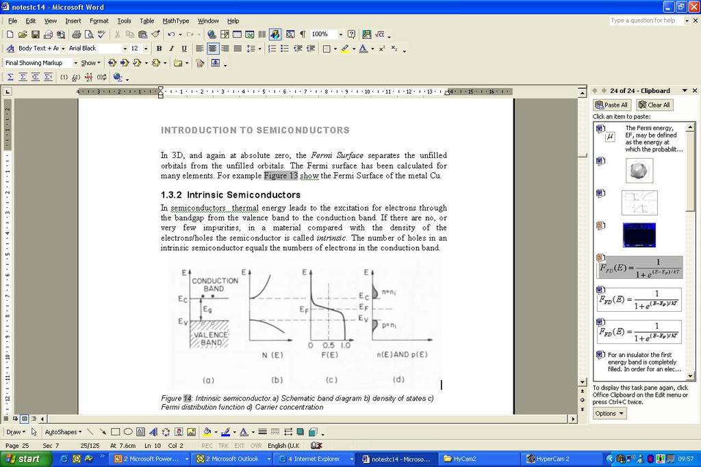
Density of states for electrons and holes. Distribution function. Conduction and valence bands
 Intrinsic Semiconductors In the field of semiconductors electrons and holes are usually referred to as free carriers, or simply carriers, because it is these particles which are responsible for carrying
David J. Starling Penn State Hazleton PHYS 214
 Being virtually killed by a virtual laser in a virtual space is just as effective as the real thing, because you are as dead as you think you are. -Douglas Adams, Mostly Harmless David J. Starling Penn
ESE 372 / Spring 2013 / Lecture 5 Metal Oxide Semiconductor Field Effect Transistor
 Metal Oxide Semiconductor Field Effect Transistor V G V G 1 Metal Oxide Semiconductor Field Effect Transistor We will need to understand how this current flows through Si What is electric current? 2 Back