Lecture (02) PN Junctions and Diodes
|
|
|
- Jody Freeman
- 6 years ago
- Views:
Transcription


1 Lecture (02) PN Junctions and Diodes By: Dr. Ahmed ElShafee ١ I Agenda N type, P type semiconductors N Type Semiconductor P Type Semiconductor PN junction Energy Diagrams of the PN Junction and Depletion Region Diode Operation VOLTAGE CURRENT CHARACTERISTIC OF A DIODE Forward bias Reverse Bias V I Characteristic for Forward Bias V I Characteristic for Reverse Bias ٢ DIODE MODELS
 must be modified by increasing the number of free electrons or holes to increase its conductivity and make it useful in electronic devices.")
2 N type, P type semiconductors Semiconductors are not good conductors because of the limited number of free electrons in the conduction band and holes in the valence band Intrinsic silicon (or germanium) must be modified by increasing the number of free electrons or holes to increase its conductivity and make it useful in electronic devices. This is done by adding impurities to the intrinsic material Two types of extrinsic (impure) semiconductive materials, n type and p type, are the key building blocks for most types of electronic devices This process, called doping, increases the number of current carriers (electrons or holes). ٣ N Type Semiconductor pentavalent (atoms with five valence electrons) impurity atoms are added. Like : arsenic (As), phosphorus (P), bismuth (Bi), and antimony (Sb). Example: Four of the antimony atom s valence electrons are used to form the covalent bonds with silicon atoms, leaving one extra electron. ٤

, indium (In), and gallium (Ga).")
3 pentavalent atom gives up an electron, it is often called a donor atom. number of conduction electrons can be controlled by the number of impurity atoms added to the silicon. doping process does not leave a hole in the valence band In N type semiconductor, the electrons are called the majority carriers. A few holes that are created when electron hole pairs are thermally generated. Holes in an n type material are called minority carriers. ٥ P Type Semiconductor To increase the number of holes in intrinsic silicon, trivalent impurity atoms are added, with three valence electrons such as boron (B), indium (In), and gallium (Ga). three of the boron atom s valence electrons are used in the covalent bonds; a hole results when each trivalent atom is added. trivalent atom can take an electron, it is often referred to as an acceptor atom. ٦
4 The number of holes can be controlled by the number of trivalent impurity atoms added to the silicon. The holes are the majority carriers in p type material. a few conduction band electrons that are created when electron hole pairs are thermally generated. Conduction band electrons in p type material are the minority carriers. ٧ PN junction When you take a block of silicon and dope part of it with a trivalent impurity and the other part with a pentavalent impurity, a boundary called the pn junction is formed between the resulting p type and n type portions. The pn junction is the basis for diodes, certain transistors, solar cells, and other devices, ٨

5 A p type material consists of silicon atoms and trivalent impurity atoms such as boron, adding a hole when it bonds with the silicon atoms. However, since the number of protons and the number of electrons are equal throughout the material, there is no net charge in the material and so it is neutral ٩ n type silicon material consists of silicon atoms and pentavalent impurity atoms, that releases an electron when it bonds with four silicon atoms still an equal number of protons and electrons, no net charge in the material and so it is neutral ١٠
. The n region has many free electrons (majority carriers) and only a few thermally generated holes (minority carriers).")

6 a pn junction forms at the boundary between the two regions and a diode is created The p region has many holes (majority carriers) and only a few thermally generated free electrons (minority carriers). The n region has many free electrons (majority carriers) and only a few thermally generated holes (minority carriers). ١١ For every electron that diffuses across the junction and combines with a hole, a positive charge is left in the n region and a negative charge is created in the p region, forming a barrier potential. This action continues until the voltage of the barrier repels further diffusion. The blue arrows between the positive and negative charges in the depletion region represent the electric field. ١٢
7 When the pn junction is formed, the n region loses free electrons as they diffuse across the junction. This creates a layer of positive charges (pentavalent ions) near the junction. the p region loses holes as the electrons and holes combine. This creates a layer of negative charges (trivalent ions) near the junction Both regions presents the depletion region ١٣ term depletion refers, region near the pn junction is depleted of charge carriers, due to diffusion across the junction. depletion region is formed very quickly and is very thin compared to the n region and p region. After the initial surge of free electrons across the pn junction, the depletion region has expanded to a point where equilibrium is established and there is no further diffusion of electrons across the junction ١٤


8 Equilibrium happens as follow: A point is reached where the total negative charge in the depletion region repels any further diffusion of electrons into the p region, and the diffusion stops. Depletion region acts as a barrier to the further movement of electrons across the junction. ١٥ Barrier Potential: Coulomb s law state that any positive charge and a negative charge near eachother, there is a force acting on the charge In the depletion region positive charges and many negative charges on opposite sides of the pn junction. The forces between the opposite charges form an electric field xternal energy must be applied to get the electrons to move across the barrier of the electric field in the depletion region. ١٦

9 Barrier Potential (volts): is The potential difference of the electric field across the depletion region is the amount of voltage required to move electrons through the electric field. The barrier potential of a pn junction depends on several factors, including the type of semiconductive material, the amount of doping, and the temperature. The typical barrier potential is approximately 0.7 V for silicon and 0.3 V for germanium at ١٧ Energy Diagrams of the PN Junction and Depletion Region The valence and conduction bands in an n type material are at slightly lower energy levels than the valence and conduction bands in a p type material. p-type material has trivalent impurities n-type material has pentavalent impurities. The trivalent impurities exert lower forces on the outershell electrons than the pentavalent impurities. The lower forces in p-type materials mean that the electron orbits are slightly larger and hence have greater energy than the electron ١٨ orbits in the n-type materials.
 and temporarily become free electrons in the lower")


10 The free electrons in the n region that occupy the upper part of the conduction band can easily diffuse across the junction (they do not have to gain additional energy) and temporarily become free electrons in the lower part of the p region conduction band. After crossing the junction, the electrons quickly lose energy and fall into the holes in the p region valence band as indicated ١٩ As the diffusion continues, the depletion region begins to form and the energy level of the n region conduction band decreases. Soon, there are no electrons left in the n region conduction band with enough energy to get across the junction to the p region conduction band, ٢٠
11 At this point, the junction is at equilibrium; and the depletion region is complete. There is an energy gradiant across the depletion region which acts as an energy hill that an n region electron must climb to get to the p region. ٢١ Notice that as the energy level of the n region conduction band has shifted downward, the energy level of the valence band has also shifted downward. It still takes the same amount of energy for a valence electron to become a free electron. In other words, the energy gap between the valence band and the conduction band remains the same. ٢٢

12 Diode Operation diode is made from a small piece of semiconductor material, usually silicon, in which half is doped as a p region and half is doped as an n region with a pn junction and depletion region in between. p region is called the anode n region is called the cathode ٢٣ ٢٤


13 Forward Bias Forward bias is the condition that allows current through the pn junction. conditions: 1. negative side of VBIAS is connected to the n region of the diode and the positive side is connected to the p region 2. A second requirement is that the bias voltage, VBIAS, must be greater than the barrier potential. The resistor limits the forward current to a value that will not damage the diode. ٢٥ the electrons are in the valence band in the p region the positive side of the bias voltage source attracts the valence electrons toward the left end of the p region, leaving holes behind on p region. The valence electrons move from one hole to the next toward the left. P region holes (majority carriers) move to the right toward the junction (attracted by depletion region), (hole current) ٢٦
14 As more electrons flow into the depletion region, the number of positive ions is reduced. As more holes effectively flow into the depletion region on the other side of the pn junction, the number of negative ions is reduced. This reduction in positive and negative ions during forward bias causes the depletion region to narrow ٢٧ As known, energy hill, is the electric field between the positive and negative ions in the depletion region, prevents free electrons from diffusing across the junction at equilibrium (barrier potential) After applying forward bais, depletion region become thin, and energy hill become smaller, ٢٨


15 As known barrier potential = 0.7 volt, Applying enough bias voltage to enable free electron to climb the potential barrier (energy hill) is 0.7 volt discounted as voltage drop over diode make depletion region disappear and enables free elections to pass through diode. ٢٩ This energy loss results in a voltage drop across the pn junction equal to the barrier potential (0.7 V An additional small voltage drop occurs across the p and n regions due to the internal resistance of the material. For doped semi conductive material, this resistance, called the dynamic resistance, is very small and can usually be neglected. ٣٠

16 Reverse Bias Reverse bias: positive side of VBIAS is connected to the n region of the diode and the negative side is connected to the p region depletion region is shown much wider than in forward bias or equilibrium ٣١ In the p region, electrons from the negative side of the voltage source enter as valence electrons and move from hole to hole toward the depletion region where they create additional negative ions. This results in a widening of the depletion region and a depletion of majority carriers. The initial flow of charge lasts for only a very short time after the reverse bias voltage is applied. ٣٢
17 As the depletion region widens, the availability of majority carriers decreases. electric field between the positive and negative ions increases in strength until the potential across the depletion region equals the bias voltage, VBIAS ٣٣ Reverse current: extremely small current that exists in reverse bias, as the small number of free minority electrons in the p region are pushed toward the pn junction by the negative bias voltage When these electrons reach the wide depletion region, they fall down the energy hill and combine with the minority holes in the n region as valence electrons and flow toward the positive bias voltage, creating a small hole current. The conduction band in the p region is at a higher energy level than the conduction band in the n region. Therefore, the minority electrons easily pass through the depletion region because they require no additional energy ٣٤

18 Reverse Breakdown if the external reverse bias voltage is increased to a value called the breakdown voltage, the reverse current will increase. high reverse bias voltage imparts energy to the free minority electrons so that as they speed through the p region, they collide with atoms with enough energy to knock valence electrons out of orbit and into the conduction band. (consider one electron collide with 2 electrons and so on) (avalanche effect) The newly created conduction electrons are also high in energy and repeat the process. ٣٥ As these high energy electrons go through the depletion region, they have enough energy to go through the n region as conduction electrons, rather than combining with holes. When the reverse current is not limited, the resulting heating will permanently damage the diode. Most diodes are not operated in reverse breakdown, but if the current is limited (by adding a series limiting resistor for example), there is no permanent damage to the diode. ٣٦


19 V I Characteristic for Forward Bias forward bias voltage is applied across a diode, current flow called forward current and is designated I F. ٣٧ With 0 V across the diode, there is no forward current increase the forward bias voltage, the forward current and the voltage across the diode gradually increase, A portion of the forward bias voltage is dropped across the () limiting resistor When Forward bias reach 0.7 volt ((barrier potential), forward current begins to increase ٣٨
20 Increasing forward bias current continues to increase very rapidly, but the voltage across the diode increases only gradually above 0.7 V (voltage drop due to diode limiting resistor) ٣٩ dynamic resistance resistance of the forward biased diode is not constant over the entire curve ٤٠
21 V I Characteristic for Reverse Bias 0 V across the diode, there is no reverse current gradually increase the reverse bias voltage, there is a very small reverse current When reverse voltage across the diode (VR) reaches the breakdown value (VBR), the reverse current begins to increase rapidly. ٤١ ٤٢
22 Temperature Effects as temperature is increased, the forward current increases for a given value of forward voltage ٤٣ DIODE MODELS Bias Connections ٤٤

23 The Ideal Diode Model: Forward biased is represented by a simple closed switch. reverse biased, is presented as open switch ٤٥ The Practical Diode Model If diode is forward biased, is equivalent to a closed switch in series with a small equivalent voltage source (VF) equal to the barrier potential (0.7 V) ٤٦


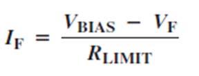
24 ٤٧ Applying KVL : Ohms law Substituting ٤٨
 and the large internal reverse resistance (r")
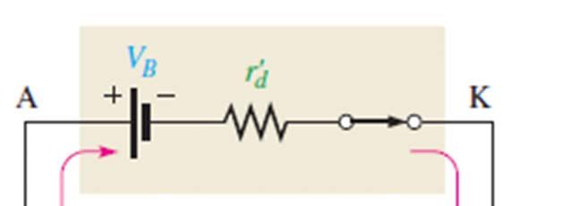
25 The Complete Diode Model Add a small forward dynamic resistance (r d) and the large internal reverse resistance (r R). ٤٩ ٥٠

26 ٥١ Example 01 ٥٢


27 Ideal model: al ٥٣ Complete model ٥٤

28 ٥٥ Ideal model Practical model: ٥٦
,")
29 Complete model ٥٧ Thanks,.. See you next week (ISA), ٥٨
Lecture (02) Introduction to Electronics II, PN Junction and Diodes I
 Introduction to Electronics II, PN Junction and Diodes I") Lecture (02) Introduction to Electronics II, PN Junction and Diodes I By: Dr. Ahmed ElShafee ١ Agenda Current in semiconductors/conductors N type, P type semiconductors N Type Semiconductor P Type Semiconductor
Lecture (02) Introduction to Electronics II, PN Junction and Diodes I By: Dr. Ahmed ElShafee ١ Agenda Current in semiconductors/conductors N type, P type semiconductors N Type Semiconductor P Type Semiconductor
Electro - Principles I
 Electro - Principles I Page 10-1 Atomic Theory It is necessary to know what goes on at the atomic level of a semiconductor so the characteristics of the semiconductor can be understood. In many cases a
Semiconductors (Chất1bán1dẫn)
") To describe the properties of n-type and p-type semiconductors and how a pn jun formed To study a diode and the characteristics of diode 1-1 Atomic Structure Atomic1Structure An atom is the smallest particle
To describe the properties of n-type and p-type semiconductors and how a pn jun formed To study a diode and the characteristics of diode 1-1 Atomic Structure Atomic1Structure An atom is the smallest particle
electronics fundamentals
 electronics fundamentals circuits, devices, and applications THOMAS L. FLOYD DAVID M. BUCHLA Lesson 1: Diodes and Applications Semiconductors Figure 1-1 The Bohr model of an atom showing electrons in orbits
Chapter 1 INTRODUCTION SEMICONDUCTORS MATERIAL
 Chapter 1 INTRODUCTION TO SEMICONDUCTORS MATERIAL Objectives Discuss basic structures of atoms Discuss properties of insulators, conductors, and semiconductors Discuss covalent bonding Describe the conductions
Electronic PRINCIPLES
 MALVINO & BATES Electronic PRINCIPLES SEVENTH EDITION Chapter 2 Semiconductors Topics Covered in Chapter 2 Conductors Semiconductors Silicon crystals Intrinsic semiconductors Two types of flow Doping a
ITT Technical Institute ET215 Devices I Unit 1
 ITT Technical Institute ET215 Devices I Unit 1 Chapter 1 Chapter 2, Sections 2.1-2.4 Chapter 1 Basic Concepts of Analog Circuits Recall ET115 & ET145 Ohms Law I = V/R If voltage across a resistor increases
CLASS 12th. Semiconductors
 CLASS 12th Semiconductors 01. Distinction Between Metals, Insulators and Semi-Conductors Metals are good conductors of electricity, insulators do not conduct electricity, while the semiconductors have
SEMICONDUCTORS. Conductivity lies between conductors and insulators. The flow of charge in a metal results from the
 SEMICONDUCTORS Conductivity lies between conductors and insulators The flow of charge in a metal results from the movement of electrons Electros are negatively charged particles (q=1.60x10⁻¹⁹ C ) The outermost
Atoms? All matters on earth made of atoms (made up of elements or combination of elements).
.") Chapter 1 Atoms? All matters on earth made of atoms (made up of elements or combination of elements). Atomic Structure Atom is the smallest particle of an element that can exist in a stable or independent
Chapter 1 Atoms? All matters on earth made of atoms (made up of elements or combination of elements). Atomic Structure Atom is the smallest particle of an element that can exist in a stable or independent
Concept of Core IENGINEERS- CONSULTANTS LECTURE NOTES SERIES ELECTRONICS ENGINEERING 1 YEAR UPTU. Page 1
 Concept of Core Conductivity of conductor and semiconductor can also be explained by concept of Core. Core: Core is a part of an atom other than its valence electrons. Core consists of all inner shells
Electronics EC /2/2012. * In-class exams: 40% 7 th week exam 25% 12 th week exam 15%
 Arab Academy for Science, Technology and Maritime Transport Electronics EC 331 Dr. Mohamed Hassan Course Assessment * In-class exams: 40% 7 th week exam 25% 12 th week exam 15% *Tutorial exams and activities:
ECE 335: Electronic Engineering Lecture 2: Semiconductors
 Faculty of Engineering ECE 335: Electronic Engineering Lecture 2: Semiconductors Agenda Intrinsic Semiconductors Extrinsic Semiconductors N-type P-type Carrier Transport Drift Diffusion Semiconductors
A SEMICONDUCTOR DIODE. P-N Junction
 A SEMICONDUCTOR DIODE P-N Junction Analog Electronics Pujianto Department of Physics Edu. State University of Yogyakarta A Semiconductor Devices A Semiconductor devices can be defined as a unit which consists,
Electronic Circuits for Mechatronics ELCT 609 Lecture 2: PN Junctions (1)
") Electronic Circuits for Mechatronics ELCT 609 Lecture 2: PN Junctions (1) Assistant Professor Office: C3.315 E-mail: eman.azab@guc.edu.eg 1 Electronic (Semiconductor) Devices P-N Junctions (Diodes): Physical
Electronic Circuits for Mechatronics ELCT 609 Lecture 2: PN Junctions (1) Assistant Professor Office: C3.315 E-mail: eman.azab@guc.edu.eg 1 Electronic (Semiconductor) Devices P-N Junctions (Diodes): Physical
3C3 Analogue Circuits
 Department of Electronic & Electrical Engineering Trinity College Dublin, 2014 3C3 Analogue Circuits Prof J K Vij jvij@tcd.ie Lecture 1: Introduction/ Semiconductors & Doping 1 Course Outline (subject
First-Hand Investigation: Modeling of Semiconductors
 perform an investigation to model the behaviour of semiconductors, including the creation of a hole or positive charge on the atom that has lost the electron and the movement of electrons and holes in
Introduction to Transistors. Semiconductors Diodes Transistors
 Introduction to Transistors Semiconductors Diodes Transistors 1 Semiconductors Typical semiconductors, like silicon and germanium, have four valence electrons which form atomic bonds with neighboring atoms
Diodes. EE223 Digital & Analogue Electronics Derek Molloy 2012/2013.
 Diodes EE223 Digital & Analogue Electronics Derek Molloy 2012/2013 Derek.Molloy@dcu.ie Diodes: A Semiconductor? Conductors Such as copper, aluminium have a cloud of free electrons weak bound valence electrons
Electronics The basics of semiconductor physics
 Electronics The basics of semiconductor physics Prof. Márta Rencz, Gergely Nagy BME DED September 16, 2013 The basic properties of semiconductors Semiconductors conductance is between that of conductors
p-n junction biasing, p-n I-V characteristics, p-n currents Norlaili Mohd. Noh EEE /09
 CLASS 6&7 p-n junction biasing, p-n I-V characteristics, p-n currents 1 p-n junction biasing Unbiased p-n junction: the potential barrier is 0.7 V for Si and 0.3 V for Ge. Nett current across the p-n junction
EE 446/646 Photovoltaic Devices I. Y. Baghzouz
 EE 446/646 Photovoltaic Devices I Y. Baghzouz What is Photovoltaics? First used in about 1890, the word has two parts: photo, derived from the Greek word for light, volt, relating to electricity pioneer
SRI VIDYA COLLEGE OF ENGINEERING AND TECHNOLOGY VIRUDHUNAGAR Department of Electronics and Communication Engineering
 SRI VIDYA COLLEGE OF ENGINEERING AND TECHNOLOGY VIRUDHUNAGAR Department of Electronics and Communication Engineering Class/Sem:I ECE/II Question Bank for EC6201-ELECTRONIC DEVICES 1.What do u meant by
Engineering 2000 Chapter 8 Semiconductors. ENG2000: R.I. Hornsey Semi: 1
 Engineering 2000 Chapter 8 Semiconductors ENG2000: R.I. Hornsey Semi: 1 Overview We need to know the electrical properties of Si To do this, we must also draw on some of the physical properties and we
PN Junction
 P Junction 2017-05-04 Definition Power Electronics = semiconductor switches are used Analogue amplifier = high power loss 250 200 u x 150 100 u Udc i 50 0 0 50 100 150 200 250 300 350 400 i,u dc i,u u
David J. Starling Penn State Hazleton PHYS 214
 Being virtually killed by a virtual laser in a virtual space is just as effective as the real thing, because you are as dead as you think you are. -Douglas Adams, Mostly Harmless David J. Starling Penn
1 1 THE ATOM. The Bohr Model HISTORY NOTE. Atomic Number
 2 INTRODUCTION TO ELECTRONICS 11 THE ATOM All matter is composed of atoms; all atoms consist of electrons, protons, and neutrons except normal hydrogen, which does not have a neutron. Each element in the
EXTRINSIC SEMICONDUCTOR
 EXTRINSIC SEMICONDUCTOR EXTRINSIC SEMICONDUCTOR A semiconductor in which the impurity atoms are added by doping process is called Extrinsic semiconductor. The addition of impurities increases the carrier
Lecture 2. Semiconductor Physics. Sunday 4/10/2015 Semiconductor Physics 1-1
 Lecture 2 Semiconductor Physics Sunday 4/10/2015 Semiconductor Physics 1-1 Outline Intrinsic bond model: electrons and holes Charge carrier generation and recombination Intrinsic semiconductor Doping:
Contents CONTENTS. Page 2 of 47
 J. A. Hargreaves Lockerbie Academy June 2015 Contents CONTENTS Contents... 2 CHAPTER 7 CONDUCTORS, SEMICONDUCTORS AND INSULATORS... 4 Summary of Content... 4 Summary of this chapter- notes from column
Higher Physics. Electricity. Summary Notes. Monitoring and measuring a.c. Current, potential difference, power and resistance
 Higher Physics Electricity Summary Notes Monitoring and measuring a.c. Current, potential difference, power and resistance Electrical sources and internal resistance Capacitors Conductors, semiconductors
BASIC ELECTRONICS CONDUCTION IN SEMICONDUCTORS
 BASIC ELECTRONICS Subject Code: ELN-15/5 IA marks: 5 Hours per week : 04 Exam Hours 03 Total Hrs: 5 Exam Marks: 100 CHAPTER 1 CONDUCTION IN SEMICONDUCTORS Electrons and holes in an intrinsic semiconductors,
Diodes. anode. cathode. cut-off. Can be approximated by a piecewise-linear-like characteristic. Lecture 9-1
 Diodes mplest nonlinear circuit element Basic operation sets the foundation for Bipolar Junction Transistors (BJTs) Also present in Field Effect Transistors (FETs) Ideal diode characteristic anode cathode
Semiconductors 1. Explain different types of semiconductors in detail with necessary bond diagrams. Intrinsic semiconductors:
 Semiconductors 1. Explain different types of semiconductors in detail with necessary bond diagrams. There are two types of semi conductors. 1. Intrinsic semiconductors 2. Extrinsic semiconductors Intrinsic
Chapter 7. The pn Junction
 Chapter 7 The pn Junction Chapter 7 PN Junction PN junction can be fabricated by implanting or diffusing donors into a P-type substrate such that a layer of semiconductor is converted into N type. Converting
ECE 340 Lecture 27 : Junction Capacitance Class Outline:
 ECE 340 Lecture 27 : Junction Capacitance Class Outline: Breakdown Review Junction Capacitance Things you should know when you leave M.J. Gilbert ECE 340 Lecture 27 10/24/11 Key Questions What types of
3.7 Physical Operation of Diodes
 10/4/2005 3_7 Physical Operation of Diodes blank.doc 1/2 3.7 Physical Operation of Diodes Reading Assignment: pp. 190200, 203205 A. Semiconductor Materials Q: So, what exactly is a junction diode made
16EC401 BASIC ELECTRONIC DEVICES UNIT I PN JUNCTION DIODE. Energy Band Diagram of Conductor, Insulator and Semiconductor:
 16EC401 BASIC ELECTRONIC DEVICES UNIT I PN JUNCTION DIODE Energy bands in Intrinsic and Extrinsic silicon: Energy Band Diagram of Conductor, Insulator and Semiconductor: 1 2 Carrier transport: Any motion
ELECTRONIC I Lecture 1 Introduction to semiconductor. By Asst. Prof Dr. Jassim K. Hmood
 ELECTRONIC I Lecture 1 Introduction to semiconductor By Asst. Prof Dr. Jassim K. Hmood SOLID-STATE ELECTRONIC MATERIALS Electronic materials generally can be divided into three categories: insulators,
LECTURE 23. MOS transistor. 1 We need a smart switch, i.e., an electronically controlled switch. Lecture Digital Circuits, Logic
 LECTURE 23 Lecture 16-20 Digital Circuits, Logic 1 We need a smart switch, i.e., an electronically controlled switch 2 We need a gain element for example, to make comparators. The device of our dreams
Electric Fields. Basic Concepts of Electricity. Ohm s Law. n An electric field applies a force to a charge. n Charges move if they are mobile
 Basic Concepts of Electricity oltage E Current I Ohm s Law Resistance R E = I R Electric Fields An electric field applies a force to a charge Force on positive charge is in direction of electric field,
Introduction to Semiconductor Physics. Prof.P. Ravindran, Department of Physics, Central University of Tamil Nadu, India
 Introduction to Semiconductor Physics 1 Prof.P. Ravindran, Department of Physics, Central University of Tamil Nadu, India http://folk.uio.no/ravi/cmp2013 Review of Semiconductor Physics Semiconductor fundamentals
Lecture 1. OUTLINE Basic Semiconductor Physics. Reading: Chapter 2.1. Semiconductors Intrinsic (undoped) silicon Doping Carrier concentrations
 silicon Doping Carrier concentrations") Lecture 1 OUTLINE Basic Semiconductor Physics Semiconductors Intrinsic (undoped) silicon Doping Carrier concentrations Reading: Chapter 2.1 EE105 Fall 2007 Lecture 1, Slide 1 What is a Semiconductor? Low
Lecture 1 OUTLINE Basic Semiconductor Physics Semiconductors Intrinsic (undoped) silicon Doping Carrier concentrations Reading: Chapter 2.1 EE105 Fall 2007 Lecture 1, Slide 1 What is a Semiconductor? Low
Introduction to Semiconductor Devices
 Physics 233 Experiment 48 Introduction to Semiconductor Devices References 1. G.W. Neudeck, The PN Junction Diode, Addison-Wesley MA 1989 2. Background notes (Appendix A) 3. Specification sheet for Diode
EE301 Electronics I , Fall
 EE301 Electronics I 2018-2019, Fall 1. Introduction to Microelectronics (1 Week/3 Hrs.) Introduction, Historical Background, Basic Consepts 2. Rewiev of Semiconductors (1 Week/3 Hrs.) Semiconductor materials
ECE 142: Electronic Circuits Lecture 3: Semiconductors
 Faculty of Engineering ECE 142: Electronic Circuits Lecture 3: Semiconductors Agenda Intrinsic Semiconductors Extrinsic Semiconductors N-type P-type Carrier Transport Drift Diffusion Semiconductors A semiconductor
Basic Physics of Semiconductors
 Basic Physics of Semiconductors Semiconductor materials and their properties PN-junction diodes Reverse Breakdown EEM 205 Electronics I Dicle University, EEE Dr. Mehmet Siraç ÖZERDEM Semiconductor Physics
Semiconductor Physics fall 2012 problems
 Semiconductor Physics fall 2012 problems 1. An n-type sample of silicon has a uniform density N D = 10 16 atoms cm -3 of arsenic, and a p-type silicon sample has N A = 10 15 atoms cm -3 of boron. For each
Unit IV Semiconductors Engineering Physics
 Introduction A semiconductor is a material that has a resistivity lies between that of a conductor and an insulator. The conductivity of a semiconductor material can be varied under an external electrical
Introduction to Semiconductor Devices
 Physics 233 Experiment 48 Introduction to Semiconductor Devices References 1. G.W. Neudeck, The PN Junction Diode, Addison-Wesley MA 1989 2. Background notes (Appendix A) 3. Specification sheet for Diode
Processing of Semiconducting Materials Prof. Pallab Banerji Department of Material Science Indian Institute of Technology, Kharagpur
 Processing of Semiconducting Materials Prof. Pallab Banerji Department of Material Science Indian Institute of Technology, Kharagpur Lecture - 4 Doping in Semiconductors Good morning. Let us start with
ECE 250 Electronic Devices 1. Electronic Device Modeling
 ECE 250 Electronic Devices 1 ECE 250 Electronic Device Modeling ECE 250 Electronic Devices 2 Introduction to Semiconductor Physics You should really take a semiconductor device physics course. We can only
Junction Diodes. Tim Sumner, Imperial College, Rm: 1009, x /18/2006
 Junction Diodes Most elementary solid state junction electronic devices. They conduct in one direction (almost correct). Useful when one converts from AC to DC (rectifier). But today diodes have a wide
Consider a uniformly doped PN junction, in which one region of the semiconductor is uniformly doped with acceptor atoms and the adjacent region is
 CHAPTER 7 The PN Junction Consider a uniformly doped PN junction, in which one region of the semiconductor is uniformly doped with acceptor atoms and the adjacent region is uniformly doped with donor atoms.
KATIHAL FİZİĞİ MNT-510
 KATIHAL FİZİĞİ MNT-510 YARIİLETKENLER Kaynaklar: Katıhal Fiziği, Prof. Dr. Mustafa Dikici, Seçkin Yayıncılık Katıhal Fiziği, Şakir Aydoğan, Nobel Yayıncılık, Physics for Computer Science Students: With
Semiconductors CHAPTER 3. Introduction The pn Junction with an Applied Voltage Intrinsic Semiconductors 136
 CHAPTER 3 Semiconductors Introduction 135 3.1 Intrinsic Semiconductors 136 3.2 Doped Semiconductors 139 3.3 Current Flow in Semiconductors 142 3.4 The pn Junction 148 3.5 The pn Junction with an Applied
ECE 442. Spring, Lecture -2
 ECE 442 Power Semiconductor Devices and Integrated circuits Spring, 2006 University of Illinois at Chicago Lecture -2 Semiconductor physics band structures and charge carriers 1. What are the types of
Introduction to Electronics and Semiconductor
 Introduction to Electronics and Semiconductor 1 Chapter Objectives To study and understand basic electronics. To study and understand semiconductor principles. 2 Definition Electronics is the branch of
Session 6: Solid State Physics. Diode
 Session 6: Solid State Physics Diode 1 Outline A B C D E F G H I J 2 Definitions / Assumptions Homojunction: the junction is between two regions of the same material Heterojunction: the junction is between
5. Semiconductors and P-N junction
 5. Semiconductors and P-N junction Thomas Zimmer, University of Bordeaux, France Summary Learning Outcomes... 2 Physical background of semiconductors... 2 The silicon crystal... 2 The energy bands... 3
n N D n p = n i p N A
 Summary of electron and hole concentration in semiconductors Intrinsic semiconductor: E G n kt i = pi = N e 2 0 Donor-doped semiconductor: n N D where N D is the concentration of donor impurity Acceptor-doped
Electronic Devices & Circuits
 Electronic Devices & Circuits For Electronics & Communication Engineering By www.thegateacademy.com Syllabus Syllabus for Electronic Devices Energy Bands in Intrinsic and Extrinsic Silicon, Carrier Transport,
Semiconductor Physics and Devices
 The pn Junction 1) Charge carriers crossing the junction. 3) Barrier potential Semiconductor Physics and Devices Chapter 8. The pn Junction Diode 2) Formation of positive and negative ions. 4) Formation
REVISED HIGHER PHYSICS REVISION BOOKLET ELECTRONS AND ENERGY
 REVSED HGHER PHYSCS REVSON BOOKLET ELECTRONS AND ENERGY Kinross High School Monitoring and measuring a.c. Alternating current: Mains supply a.c.; batteries/cells supply d.c. Electrons moving back and forth,
SOLID STATE ELECTRONICS DIGITAL ELECTRONICS SOFT CONDENSED MATTER PHYSICS
 SOLID STATE ELECTRONICS DIGITAL ELECTRONICS SOFT CONDENSED MATTER PHYSICS The energy band occupied by the valence electrons is called valence band and is the highest filled band. Bnd occupied by the electrons
Chapter 1 Overview of Semiconductor Materials and Physics
 Chapter 1 Overview of Semiconductor Materials and Physics Professor Paul K. Chu Conductivity / Resistivity of Insulators, Semiconductors, and Conductors Semiconductor Elements Period II III IV V VI 2 B
CLASS 1 & 2 REVISION ON SEMICONDUCTOR PHYSICS. Reference: Electronic Devices by Floyd
 CLASS 1 & 2 REVISION ON SEMICONDUCTOR PHYSICS Reference: Electronic Devices by Floyd 1 ELECTRONIC DEVICES Diodes, transistors and integrated circuits (IC) are typical devices in electronic circuits. All
ELECTRONIC DEVICES AND CIRCUITS SUMMARY
 ELECTRONIC DEVICES AND CIRCUITS SUMMARY Classification of Materials: Insulator: An insulator is a material that offers a very low level (or negligible) of conductivity when voltage is applied. Eg: Paper,
Determination of properties in semiconductor materials by applying Matlab
 Determination of properties in semiconductor materials by applying Matlab Carlos Figueroa. 1, Raúl Riera A. 2 1 Departamento de Ingeniería Industrial. Universidad de Sonora A.P. 5-088, Hermosillo, Sonora.
CEMTool Tutorial. Semiconductor physics
 EMTool Tutorial Semiconductor physics Overview This tutorial is part of the EMWARE series. Each tutorial in this series will teach you a specific topic of common applications by explaining theoretical
ECE-342 Test 2 Solutions, Nov 4, :00-8:00pm, Closed Book (one page of notes allowed)
") ECE-342 Test 2 Solutions, Nov 4, 2008 6:00-8:00pm, Closed Book (one page of notes allowed) Please use the following physical constants in your calculations: Boltzmann s Constant: Electron Charge: Free
ECE-342 Test 2 Solutions, Nov 4, 2008 6:00-8:00pm, Closed Book (one page of notes allowed) Please use the following physical constants in your calculations: Boltzmann s Constant: Electron Charge: Free
FREQUENTLY ASKED QUESTIONS February 21, 2017
 FREQUENTLY ASKED QUESTIONS February 21, 2017 Content Questions How do you place a single arsenic atom with the ratio 1 in 100 million? Sounds difficult to get evenly spread throughout. Yes, techniques
Semi-Conductors insulators semi-conductors N-type Semi-Conductors P-type Semi-Conductors
 Semi-Conductors In the metal materials considered earlier, the coupling of the atoms together to form the material decouples an electron from each atom setting it free to roam around inside the material.
This is the 15th lecture of this course in which we begin a new topic, Excess Carriers. This topic will be covered in two lectures.
 Solid State Devices Dr. S. Karmalkar Department of Electronics and Communication Engineering Indian Institute of Technology, Madras Lecture - 15 Excess Carriers This is the 15th lecture of this course
A semiconductor is an almost insulating material, in which by contamination (doping) positive or negative charge carriers can be introduced.
 positive or negative charge carriers can be introduced.") Semiconductor A semiconductor is an almost insulating material, in which by contamination (doping) positive or negative charge carriers can be introduced. Page 2 Semiconductor materials Page 3 Energy levels
Semiconductor A semiconductor is an almost insulating material, in which by contamination (doping) positive or negative charge carriers can be introduced. Page 2 Semiconductor materials Page 3 Energy levels
ESE370: Circuit-Level Modeling, Design, and Optimization for Digital Systems
 ESE370: Circuit-Level Modeling, Design, and Optimization for Digital Systems Lec 6: September 14, 2015 MOS Model You are Here: Transistor Edition! Previously: simple models (0 and 1 st order) " Comfortable
ISSUES TO ADDRESS...
 Chapter 12: Electrical Properties School of Mechanical Engineering Choi, Hae-Jin Materials Science - Prof. Choi, Hae-Jin Chapter 12-1 ISSUES TO ADDRESS... How are electrical conductance and resistance
SEMICONDUCTOR DIODE. Unbiased (non-polarized) PN junction
 PN junction") SEMICONDUCTOR DIODE Semiconductor diode is an electronic element made of different types of extrinsic semiconductor: N-type semiconductor doped by donor impurities and P-type semiconductor doped by acceptor
SEMICONDUCTOR DIODE Semiconductor diode is an electronic element made of different types of extrinsic semiconductor: N-type semiconductor doped by donor impurities and P-type semiconductor doped by acceptor
Semiconductor Detectors
 Semiconductor Detectors Summary of Last Lecture Band structure in Solids: Conduction band Conduction band thermal conductivity: E g > 5 ev Valence band Insulator Charge carrier in conductor: e - Charge
Current mechanisms Exam January 27, 2012
 Current mechanisms Exam January 27, 2012 There are four mechanisms that typically cause currents to flow: thermionic emission, diffusion, drift, and tunneling. Explain briefly which kind of current mechanisms
smal band gap Saturday, April 9, 2011
 small band gap upper (conduction) band empty small gap valence band filled 2s 2p 2s 2p hybrid (s+p)band 2p no gap 2s (depend on the crystallographic orientation) extrinsic semiconductor semi-metal electron
The Periodic Table III IV V
 The Periodic Table III IV V Slide 1 Electronic Bonds in Silicon 2-D picture of perfect crystal of pure silicon; double line is a Si-Si bond with each line representing an electron Si ion (charge +4 q)
UNIVERSITY OF CALIFORNIA College of Engineering Department of Electrical Engineering and Computer Sciences. EECS 130 Professor Ali Javey Fall 2006
 UNIVERSITY OF CALIFORNIA College of Engineering Department of Electrical Engineering and Computer Sciences EECS 130 Professor Ali Javey Fall 2006 Midterm I Name: Closed book. One sheet of notes is allowed.
Semiconductor Physics fall 2012 problems
 Semiconductor Physics fall 2012 problems 1. An n-type sample of silicon has a uniform density N D = 10 16 atoms cm -3 of arsenic, and a p-type silicon sample has N A = 10 15 atoms cm -3 of boron. For each
For the following statements, mark ( ) for true statement and (X) for wrong statement and correct it.
 for true statement and (X) for wrong statement and correct it.") Benha University Faculty of Engineering Shoubra Electrical Engineering Department First Year communications. Answer all the following questions Illustrate your answers with sketches when necessary. The
Benha University Faculty of Engineering Shoubra Electrical Engineering Department First Year communications. Answer all the following questions Illustrate your answers with sketches when necessary. The
Ga and P Atoms to Covalent Solid GaP
 Ga and P Atoms to Covalent Solid GaP Band Gaps in Binary Group III-V Semiconductors Mixed Semiconductors Affect of replacing some of the As with P in GaAs Band Gap (ev) (nm) GaAs 1.35 919 (IR) GaP 2.24
Review Energy Bands Carrier Density & Mobility Carrier Transport Generation and Recombination
 Review Energy Bands Carrier Density & Mobility Carrier Transport Generation and Recombination The Metal-Semiconductor Junction: Review Energy band diagram of the metal and the semiconductor before (a)
Effective masses in semiconductors
 Effective masses in semiconductors The effective mass is defined as: In a solid, the electron (hole) effective mass represents how electrons move in an applied field. The effective mass reflects the inverse
Semiconductor Devices and Circuits Fall Midterm Exam. Instructor: Dr. Dietmar Knipp, Professor of Electrical Engineering. Name: Mat. -Nr.
 Semiconductor Devices and Circuits Fall 2003 Midterm Exam Instructor: Dr. Dietmar Knipp, Professor of Electrical Engineering Name: Mat. -Nr.: Guidelines: Duration of the Midterm: 1 hour The exam is a closed
Solid State Electronics. Final Examination
 The University of Toledo EECS:4400/5400/7400 Solid State Electronic Section elssf08fs.fm - 1 Solid State Electronics Final Examination Problems Points 1. 1. 14 3. 14 Total 40 Was the exam fair? yes no
Electrons are shared in covalent bonds between atoms of Si. A bound electron has the lowest energy state.
 Photovoltaics Basic Steps the generation of light-generated carriers; the collection of the light-generated carriers to generate a current; the generation of a large voltage across the solar cell; and
Qualitative Picture of the Ideal Diode. G.R. Tynan UC San Diego MAE 119 Lecture Notes
 Qualitative Picture of the Ideal Diode G.R. Tynan UC San Diego MAE 119 Lecture Notes Band Theory of Solids: From Single Attoms to Solid Crystals Isolated Li atom (conducting metal) Has well-defined, isolated
ECE321 Electronics I
 ECE321 Electronics I Lecture 4: Physics of Semiconductor iodes Payman Zarkesh-Ha Office: ECE Bldg. 230B Office hours: Tuesday 2:00-3:00PM or by appointment E-mail: pzarkesh.unm.edu Slide: 1 Review of Last
Carriers Concentration in Semiconductors - V. Prof.P. Ravindran, Department of Physics, Central University of Tamil Nadu, India
 Carriers Concentration in Semiconductors - V 1 Prof.P. Ravindran, Department of Physics, Central University of Tamil Nadu, India http://folk.uio.no/ravi/semi2013 Motion and Recombination of Electrons and
Semiconductors. Semiconductors also can collect and generate photons, so they are important in optoelectronic or photonic applications.
 Semiconductors Semiconducting materials have electrical properties that fall between true conductors, (like metals) which are always highly conducting and insulators (like glass or plastic or common ceramics)
e - Galvanic Cell 1. Voltage Sources 1.1 Polymer Electrolyte Membrane (PEM) Fuel Cell
 Fuel Cell") Galvanic cells convert different forms of energy (chemical fuel, sunlight, mechanical pressure, etc.) into electrical energy and heat. In this lecture, we are interested in some examples of galvanic cells.
Galvanic cells convert different forms of energy (chemical fuel, sunlight, mechanical pressure, etc.) into electrical energy and heat. In this lecture, we are interested in some examples of galvanic cells.
Misan University College of Engineering Electrical Engineering Department. Exam: Final semester Date: 17/6/2017
 Misan University College of Engineering Electrical Engineering Department Subject: Electronic I Class: 1 st stage Exam: Final semester Date: 17/6/2017 Examiner: Dr. Baqer. O. TH. Time: 3 hr. Note: Answer
EECS130 Integrated Circuit Devices
 EECS130 Integrated Circuit Devices Professor Ali Javey 9/18/2007 P Junctions Lecture 1 Reading: Chapter 5 Announcements For THIS WEEK OLY, Prof. Javey's office hours will be held on Tuesday, Sept 18 3:30-4:30
Charge Carriers in Semiconductor
 Charge Carriers in Semiconductor To understand PN junction s IV characteristics, it is important to understand charge carriers behavior in solids, how to modify carrier densities, and different mechanisms
collisions of electrons. In semiconductor, in certain temperature ranges the conductivity increases rapidly by increasing temperature
 1.9. Temperature Dependence of Semiconductor Conductivity Such dependence is one most important in semiconductor. In metals, Conductivity decreases by increasing temperature due to greater frequency of