ESE 372 / Spring 2013 / Lecture 5 Metal Oxide Semiconductor Field Effect Transistor
|
|
|
- Alannah McDaniel
- 5 years ago
- Views:
Transcription

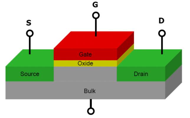
1 Metal Oxide Semiconductor Field Effect Transistor V G V G 1
2 Metal Oxide Semiconductor Field Effect Transistor We will need to understand how this current flows through Si What is electric current? 2
3 Back to atom E 3 E 2 E 1 P 3 P 2 P 1 Electron near nucleus in atom can have only certain set of shapes of probability density functions. Each of them corresponds to different bond energy. In order to release electron from ground state in atom one has to spend energy E 1. In hydrogen this energy is ~13.6 ev. 3
4 Two atoms together Simple model of crystal A lot of atoms together Bands of energy levels 4


5 Semiconductors Once temperature is increased above absolute zero the vibration of lattice can excite electrons from valence band into conduction band and two types of mobile charges would appear: 1. Electrons in conduction band; 2. Holes in valence band. These quasi particles can move and thus give rise to electric current. We will need to learn how to calculate the concentrations of free electrons and holes. 5
6 Concentration of electrons in conduction band Top of conduction band Top of conduction band Density of states - Number of allowed states per unit energy per unit volume Probability of having electron at state with energy E. Number of electrons in energy interval de near energy E in crystal of unit volume: 6
7 Probability of having electron at energy E. Boltzmann's constant Now let s take into account the fact that for transition to occur one has to have electron in original state. Probability that electron is at E 1. Probability that electron is at E 2. 7
8 Fermi Dirac distribution function In equilibrium: hence Fermi energy 8
9 Concentration of electrons in conduction band HERE THERE ARE ALLOWED STATES AND NONZERO PROBABILITY OF HAVING ELECTRONS Density of states - Number of allowed states per unit energy per unit volume??? Fermi-Dirac distribution function 9

10 Consider crystal of volume Density of states From uncertainty principle hence Volume in momentum space per state: Two electrons per state (Paoli s exclusion principle) Number of states with momentum : Kinetic energy of electron in conduction band Density of states number of states per unit energy per unit volume. Electron s effective mass 10
11 Electron and Hole concentrations 11

12 Boltzmann s approximation Can not be taken analytically Fortunately for for Effective density of states at band edge 12
13 Electron and hole concentrations. 13
14 Intrinsic semiconductors 14


15 Drift Current in intrinsic Si Average time between collisions Electron mobility 15

16 Doping Intrinsic N-type P-type P donor atom P has 5 electrons, four of them are used to complete chemical bonds and one remains loosely bound to P. B acceptor atom B has 3 electrons, can still one extra to complete chemical bonds. Concentration of donor atoms Concentration of acceptor atoms 16
17 Doped Semiconductors N-type P-type 17
18 Drift current in n type Positive voltage means increased potential energy of positively charged particle Potential energy of negatively charged particle, i.e. electron 18
19 Diffusion current Flux of electrons from left to right: Diffusion coefficient 19
20 N type in equilibrium Einstein relationship: Hence 20
21 Excess (nonequilibrium) charge carriers Equilibrium Shine light with photon energy > bandgap Nonequilibrium Quasi-Fermi levels Steady-state nonequilibrium carrier concentration will be determined by light intensity and carrier lifetime. 21
22 Excess (nonequilibrium) charge carriers Once excitation is removed the carrier concentrations will decay to their equilibrium values. carrier lifetime 22
23 Inject excess carriers Diffusion current density Assume no electric field and observe that carriers recombine as they move due to diffusion 23

24 Diffusion length Electron concentration can change in time only if or due to recombination. - Continuity equation In case of diffusion: In steady-state: Diffusion length 24
Semiconductor Physics. Lecture 3
 Semiconductor Physics Lecture 3 Intrinsic carrier density Intrinsic carrier density Law of mass action Valid also if we add an impurity which either donates extra electrons or holes the number of carriers
PN Junction
 P Junction 2017-05-04 Definition Power Electronics = semiconductor switches are used Analogue amplifier = high power loss 250 200 u x 150 100 u Udc i 50 0 0 50 100 150 200 250 300 350 400 i,u dc i,u u
Due to the quantum nature of electrons, one energy state can be occupied only by one electron.
 In crystalline solids, not all values of the electron energy are possible. The allowed intervals of energy are called allowed bands (shown as blue and chess-board blue). The forbidden intervals are called
The German University in Cairo. Faculty of Information Engineering & Technology Semiconductors (Elct 503) Electronics Department Fall 2014
 Electronics Department Fall 2014") The German University in Cairo th Electronics 5 Semester Faculty of Information Engineering & Technology Semiconductors (Elct 503) Electronics Department Fall 2014 Problem Set 3 1- a) Find the resistivity
The German University in Cairo th Electronics 5 Semester Faculty of Information Engineering & Technology Semiconductors (Elct 503) Electronics Department Fall 2014 Problem Set 3 1- a) Find the resistivity
Session 5: Solid State Physics. Charge Mobility Drift Diffusion Recombination-Generation
 Session 5: Solid State Physics Charge Mobility Drift Diffusion Recombination-Generation 1 Outline A B C D E F G H I J 2 Mobile Charge Carriers in Semiconductors Three primary types of carrier action occur
The photovoltaic effect occurs in semiconductors where there are distinct valence and
 How a Photovoltaic Cell Works The photovoltaic effect occurs in semiconductors where there are distinct valence and conduction bands. (There are energies at which electrons can not exist within the solid)
n N D n p = n i p N A
 Summary of electron and hole concentration in semiconductors Intrinsic semiconductor: E G n kt i = pi = N e 2 0 Donor-doped semiconductor: n N D where N D is the concentration of donor impurity Acceptor-doped
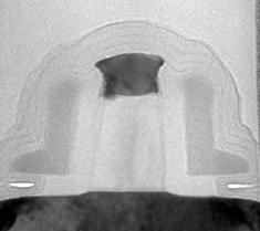
EE143 Fall 2016 Microfabrication Technologies. Evolution of Devices
 EE143 Fall 2016 Microfabrication Technologies Prof. Ming C. Wu wu@eecs.berkeley.edu 511 Sutardja Dai Hall (SDH) 1-1 Evolution of Devices Yesterday s Transistor (1947) Today s Transistor (2006) 1-2 1 Why
ECE 250 Electronic Devices 1. Electronic Device Modeling
 ECE 250 Electronic Devices 1 ECE 250 Electronic Device Modeling ECE 250 Electronic Devices 2 Introduction to Semiconductor Physics You should really take a semiconductor device physics course. We can only
Chapter 1 Overview of Semiconductor Materials and Physics
 Chapter 1 Overview of Semiconductor Materials and Physics Professor Paul K. Chu Conductivity / Resistivity of Insulators, Semiconductors, and Conductors Semiconductor Elements Period II III IV V VI 2 B
Semiconductor Devices and Circuits Fall Midterm Exam. Instructor: Dr. Dietmar Knipp, Professor of Electrical Engineering. Name: Mat. -Nr.
 Semiconductor Devices and Circuits Fall 2003 Midterm Exam Instructor: Dr. Dietmar Knipp, Professor of Electrical Engineering Name: Mat. -Nr.: Guidelines: Duration of the Midterm: 1 hour The exam is a closed
Carriers Concentration and Current in Semiconductors
 Carriers Concentration and Current in Semiconductors Carrier Transport Two driving forces for carrier transport: electric field and spatial variation of the carrier concentration. Both driving forces lead
In this block the two transport mechanisms will be discussed: diffusion and drift.
 ET3034TUx - 2.3.3 Transport of charge carriers What are the charge carrier transport principles? In this block the two transport mechanisms will be discussed: diffusion and drift. We will discuss that
Lecture 2. Semiconductor Physics. Sunday 4/10/2015 Semiconductor Physics 1-1
 Lecture 2 Semiconductor Physics Sunday 4/10/2015 Semiconductor Physics 1-1 Outline Intrinsic bond model: electrons and holes Charge carrier generation and recombination Intrinsic semiconductor Doping:
Charge Carriers in Semiconductor
 Charge Carriers in Semiconductor To understand PN junction s IV characteristics, it is important to understand charge carriers behavior in solids, how to modify carrier densities, and different mechanisms
Appendix 1: List of symbols
 Appendix 1: List of symbols Symbol Description MKS Units a Acceleration m/s 2 a 0 Bohr radius m A Area m 2 A* Richardson constant m/s A C Collector area m 2 A E Emitter area m 2 b Bimolecular recombination
Nature of Lesson (Lecture/Tutorial) H3 WK No. Day/ Date. Remarks. Duration. 4.00pm 6.30pm ALL. 2.5 hours. Introduction to Semiconductors Lecture 01
 H3 WK No. Day/ Date. Remarks. Duration. 4.00pm 6.30pm ALL. 2.5 hours. Introduction to Semiconductors Lecture 01") JANUARY 2018 INTAKE Subject : Semiconductor Physics & Devices Venue : HCI Schedule : Mondays for Tutorial (3pm 5pm / 5pm 7pm) or Tuesdays for Tutorial (3pm 5pm / 5pm 7pm) and Thursdays for Lecture (4pm-6.30
JANUARY 2018 INTAKE Subject : Semiconductor Physics & Devices Venue : HCI Schedule : Mondays for Tutorial (3pm 5pm / 5pm 7pm) or Tuesdays for Tutorial (3pm 5pm / 5pm 7pm) and Thursdays for Lecture (4pm-6.30
collisions of electrons. In semiconductor, in certain temperature ranges the conductivity increases rapidly by increasing temperature
 1.9. Temperature Dependence of Semiconductor Conductivity Such dependence is one most important in semiconductor. In metals, Conductivity decreases by increasing temperature due to greater frequency of
Ch. 2: Energy Bands And Charge Carriers In Semiconductors
 Ch. 2: Energy Bands And Charge Carriers In Semiconductors Discrete energy levels arise from balance of attraction force between electrons and nucleus and repulsion force between electrons each electron
ECE 442. Spring, Lecture -2
 ECE 442 Power Semiconductor Devices and Integrated circuits Spring, 2006 University of Illinois at Chicago Lecture -2 Semiconductor physics band structures and charge carriers 1. What are the types of
Semiconductor Physics
 Semiconductor Physics Motivation Is it possible that there might be current flowing in a conductor (or a semiconductor) even when there is no potential difference supplied across its ends? Look at the
Classification of Solids
 Classification of Solids Classification by conductivity, which is related to the band structure: (Filled bands are shown dark; D(E) = Density of states) Class Electron Density Density of States D(E) Examples
EE 346: Semiconductor Devices
 EE 346: Semiconductor Devices Lecture - 6 02/06/2017 Tewodros A. Zewde 1 DENSTY OF STATES FUNCTON Since current is due to the flow of charge, an important step in the process is to determine the number
Direct and Indirect Semiconductor
 Direct and Indirect Semiconductor Allowed values of energy can be plotted vs. the propagation constant, k. Since the periodicity of most lattices is different in various direction, the E-k diagram must
ET3034TUx Utilization of band gap energy
 ET3034TUx - 3.3.1 - Utilization of band gap energy In the last two weeks we have discussed the working principle of a solar cell and the external parameters that define the performance of a solar cell.
Crystal Properties. MS415 Lec. 2. High performance, high current. ZnO. GaN
 Crystal Properties Crystal Lattices: Periodic arrangement of atoms Repeated unit cells (solid-state) Stuffing atoms into unit cells Determine mechanical & electrical properties High performance, high current
ECE 606 Homework Week 7 Mark Lundstrom Purdue University (revised 2/25/13) e E i! E T
 e E i! E T") ECE 606 Homework Week 7 Mark Lundstrom Purdue University (revised 2/25/13) 1) Consider an n- type semiconductor for which the only states in the bandgap are donor levels (i.e. ( E T = E D ). Begin with
ECE 606 Homework Week 7 Mark Lundstrom Purdue University (revised 2/25/13) 1) Consider an n- type semiconductor for which the only states in the bandgap are donor levels (i.e. ( E T = E D ). Begin with
Quiz #1 Practice Problem Set
 Name: Student Number: ELEC 3908 Physical Electronics Quiz #1 Practice Problem Set? Minutes January 22, 2016 - No aids except a non-programmable calculator - All questions must be answered - All questions
EECS143 Microfabrication Technology
 EECS143 Microfabrication Technology Professor Ali Javey Introduction to Materials Lecture 1 Evolution of Devices Yesterday s Transistor (1947) Today s Transistor (2006) Why Semiconductors? Conductors e.g
UNIVERSITY OF CALIFORNIA College of Engineering Department of Electrical Engineering and Computer Sciences. EECS 130 Professor Ali Javey Fall 2006
 UNIVERSITY OF CALIFORNIA College of Engineering Department of Electrical Engineering and Computer Sciences EECS 130 Professor Ali Javey Fall 2006 Midterm I Name: Closed book. One sheet of notes is allowed.
Basic cell design. Si cell
 Basic cell design Si cell 1 Concepts needed to describe photovoltaic device 1. energy bands in semiconductors: from bonds to bands 2. free carriers: holes and electrons, doping 3. electron and hole current:
Semiconductor Physics fall 2012 problems
 Semiconductor Physics fall 2012 problems 1. An n-type sample of silicon has a uniform density N D = 10 16 atoms cm -3 of arsenic, and a p-type silicon sample has N A = 10 15 atoms cm -3 of boron. For each
EECS130 Integrated Circuit Devices
 EECS130 Integrated Circuit Devices Professor Ali Javey 8/30/2007 Semiconductor Fundamentals Lecture 2 Read: Chapters 1 and 2 Last Lecture: Energy Band Diagram Conduction band E c E g Band gap E v Valence
The Semiconductor in Equilibrium
 Lecture 6 Semiconductor physics IV The Semiconductor in Equilibrium Equilibrium, or thermal equilibrium No external forces such as voltages, electric fields. Magnetic fields, or temperature gradients are
Carrier Recombination
 Notes for ECE-606: Spring 013 Carrier Recombination Professor Mark Lundstrom Electrical and Computer Engineering Purdue University, West Lafayette, IN USA lundstro@purdue.edu /19/13 1 carrier recombination-generation
Engineering 2000 Chapter 8 Semiconductors. ENG2000: R.I. Hornsey Semi: 1
 Engineering 2000 Chapter 8 Semiconductors ENG2000: R.I. Hornsey Semi: 1 Overview We need to know the electrical properties of Si To do this, we must also draw on some of the physical properties and we
Chemistry Instrumental Analysis Lecture 8. Chem 4631
 Chemistry 4631 Instrumental Analysis Lecture 8 UV to IR Components of Optical Basic components of spectroscopic instruments: stable source of radiant energy transparent container to hold sample device
PHYS208 P-N Junction. Olav Torheim. May 30, 2007
 1 PHYS208 P-N Junction Olav Torheim May 30, 2007 1 Intrinsic semiconductors The lower end of the conduction band is a parabola, just like in the quadratic free electron case (E = h2 k 2 2m ). The density
L5: Surface Recombination, Continuity Equation & Extended Topics tanford University
 L5: Surface Recombination, Continuity Equation & Extended Topics EE 216 : Aneesh Nainani 1 Announcements Project Select topic by Jan 29 (Tuesday) 9 topics, maximum 4 students per topic Quiz Thursday (Jan
Note that it is traditional to draw the diagram for semiconductors rotated 90 degrees, i.e. the version on the right above.
 5 Semiconductors The nearly free electron model applies equally in the case where the Fermi level lies within a small band gap (semiconductors), as it does when the Fermi level lies within a band (metal)
Basic Semiconductor Physics
 6 Basic Semiconductor Physics 6.1 Introduction With this chapter we start with the discussion of some important concepts from semiconductor physics, which are required to understand the operation of solar
Lecture 8. Equations of State, Equilibrium and Einstein Relationships and Generation/Recombination
 Lecture 8 Equations of State, Equilibrium and Einstein Relationships and Generation/Recombination Reading: (Cont d) Notes and Anderson 2 sections 3.4-3.11 Energy Equilibrium Concept Consider a non-uniformly
PHYS208 p-n junction. January 15, 2010
 1 PHYS208 p-n junction January 15, 2010 List of topics (1) Density of states Fermi-Dirac distribution Law of mass action Doped semiconductors Dopinglevel p-n-junctions 1 Intrinsic semiconductors List of
Introduction to Engineering Materials ENGR2000. Dr.Coates
 Introduction to Engineering Materials ENGR2000 Chapter 18: Electrical Properties Dr.Coates 18.2 Ohm s Law V = IR where R is the resistance of the material, V is the voltage and I is the current. l R A
Carriers Concentration in Semiconductors - V. Prof.P. Ravindran, Department of Physics, Central University of Tamil Nadu, India
 Carriers Concentration in Semiconductors - V 1 Prof.P. Ravindran, Department of Physics, Central University of Tamil Nadu, India http://folk.uio.no/ravi/semi2013 Motion and Recombination of Electrons and
Recitation 2: Equilibrium Electron and Hole Concentration from Doping
 Recitation : Equilibrium Electron and Hole Concentration from Doping Here is a list of new things we learned yesterday: 1. Electrons and Holes. Generation and Recombination 3. Thermal Equilibrium 4. Law
Lecture 1. OUTLINE Basic Semiconductor Physics. Reading: Chapter 2.1. Semiconductors Intrinsic (undoped) silicon Doping Carrier concentrations
 silicon Doping Carrier concentrations") Lecture 1 OUTLINE Basic Semiconductor Physics Semiconductors Intrinsic (undoped) silicon Doping Carrier concentrations Reading: Chapter 2.1 EE105 Fall 2007 Lecture 1, Slide 1 What is a Semiconductor? Low
Lecture 1 OUTLINE Basic Semiconductor Physics Semiconductors Intrinsic (undoped) silicon Doping Carrier concentrations Reading: Chapter 2.1 EE105 Fall 2007 Lecture 1, Slide 1 What is a Semiconductor? Low
This is the 15th lecture of this course in which we begin a new topic, Excess Carriers. This topic will be covered in two lectures.
 Solid State Devices Dr. S. Karmalkar Department of Electronics and Communication Engineering Indian Institute of Technology, Madras Lecture - 15 Excess Carriers This is the 15th lecture of this course
Review of Semiconductor Fundamentals
 ECE 541/ME 541 Microelectronic Fabrication Techniques Review of Semiconductor Fundamentals Zheng Yang (ERF 3017, email: yangzhen@uic.edu) Page 1 Semiconductor A semiconductor is an almost insulating material,
Chapter 1 Semiconductor basics
 Chapter 1 Semiconductor basics ELEC-H402/CH1: Semiconductor basics 1 Basic semiconductor concepts Semiconductor basics Semiconductors, silicon and hole-electron pair Intrinsic silicon properties Doped
EE 446/646 Photovoltaic Devices I. Y. Baghzouz
 EE 446/646 Photovoltaic Devices I Y. Baghzouz What is Photovoltaics? First used in about 1890, the word has two parts: photo, derived from the Greek word for light, volt, relating to electricity pioneer
Semiconductor Physics and Devices
 The pn Junction 1) Charge carriers crossing the junction. 3) Barrier potential Semiconductor Physics and Devices Chapter 8. The pn Junction Diode 2) Formation of positive and negative ions. 4) Formation
8.1 Drift diffusion model
 8.1 Drift diffusion model Advanced theory 1 Basic Semiconductor Equations The fundamentals of semiconductor physic are well described by tools of quantum mechanic. This point of view gives us a model of
Lecture 3b. Bonding Model and Dopants. Reading: (Cont d) Notes and Anderson 2 sections
 Notes and Anderson 2 sections") Lecture 3b Bonding Model and Dopants Reading: (Cont d) Notes and Anderson 2 sections 2.3-2.7 The need for more control over carrier concentration Without help the total number of carriers (electrons and
Lecture 3b Bonding Model and Dopants Reading: (Cont d) Notes and Anderson 2 sections 2.3-2.7 The need for more control over carrier concentration Without help the total number of carriers (electrons and
CME 300 Properties of Materials. ANSWERS: Homework 9 November 26, As atoms approach each other in the solid state the quantized energy states:
 CME 300 Properties of Materials ANSWERS: Homework 9 November 26, 2011 As atoms approach each other in the solid state the quantized energy states: are split. This splitting is associated with the wave
1 Name: Student number: DEPARTMENT OF PHYSICS AND PHYSICAL OCEANOGRAPHY MEMORIAL UNIVERSITY OF NEWFOUNDLAND. Fall :00-11:00
 1 Name: DEPARTMENT OF PHYSICS AND PHYSICAL OCEANOGRAPHY MEMORIAL UNIVERSITY OF NEWFOUNDLAND Final Exam Physics 3000 December 11, 2012 Fall 2012 9:00-11:00 INSTRUCTIONS: 1. Answer all seven (7) questions.
Semiconductors 1. Explain different types of semiconductors in detail with necessary bond diagrams. Intrinsic semiconductors:
 Semiconductors 1. Explain different types of semiconductors in detail with necessary bond diagrams. There are two types of semi conductors. 1. Intrinsic semiconductors 2. Extrinsic semiconductors Intrinsic
SEMICONDUCTOR PHYSICS REVIEW BONDS,
 SEMICONDUCTOR PHYSICS REVIEW BONDS, BANDS, EFFECTIVE MASS, DRIFT, DIFFUSION, GENERATION, RECOMBINATION February 3, 2011 The University of Toledo, Department of Physics and Astronomy SSARE, PVIC Principles
Section 12: Intro to Devices
 Section 12: Intro to Devices Extensive reading materials on reserve, including Robert F. Pierret, Semiconductor Device Fundamentals Bond Model of Electrons and Holes Si Si Si Si Si Si Si Si Si Silicon
Lecture 15: Optoelectronic devices: Introduction
 Lecture 15: Optoelectronic devices: Introduction Contents 1 Optical absorption 1 1.1 Absorption coefficient....................... 2 2 Optical recombination 5 3 Recombination and carrier lifetime 6 3.1
3.1 Introduction to Semiconductors. Y. Baghzouz ECE Department UNLV
 3.1 Introduction to Semiconductors Y. Baghzouz ECE Department UNLV Introduction In this lecture, we will cover the basic aspects of semiconductor materials, and the physical mechanisms which are at the
HALL EFFECT IN SEMICONDUCTORS
 Warsaw University of Technology Faculty of Physics Physics Laboratory I P Andrzej Kubiaczyk 30 HALL EFFECT IN SEMICONDUCTORS 1. ackground 1.1. Electron motion in electric and magnetic fields A particle
Isolated atoms Hydrogen Energy Levels. Neuromorphic Engineering I. Solids Energy bands. Metals, semiconductors and insulators Energy bands
 Isolated atoms Hydrogen Energy Levels Neuromorphic Engineering I INI-404 227-1033-00 Electron in atoms have quantized energy levels Material courtesy of Elisabetta Chicca Bielefeld University, Germany
ECE 335: Electronic Engineering Lecture 2: Semiconductors
 Faculty of Engineering ECE 335: Electronic Engineering Lecture 2: Semiconductors Agenda Intrinsic Semiconductors Extrinsic Semiconductors N-type P-type Carrier Transport Drift Diffusion Semiconductors
Semiconductor Physics and Devices Chapter 3.
 Introduction to the Quantum Theory of Solids We applied quantum mechanics and Schrödinger s equation to determine the behavior of electrons in a potential. Important findings Semiconductor Physics and
CONTENTS. vii. CHAPTER 2 Operators 15
 CHAPTER 1 Why Quantum Mechanics? 1 1.1 Newtonian Mechanics and Classical Electromagnetism 1 (a) Newtonian Mechanics 1 (b) Electromagnetism 2 1.2 Black Body Radiation 3 1.3 The Heat Capacity of Solids and
Minimal Update of Solid State Physics
 Minimal Update of Solid State Physics It is expected that participants are acquainted with basics of solid state physics. Therefore here we will refresh only those aspects, which are absolutely necessary
Spring Semester 2012 Final Exam
 Spring Semester 2012 Final Exam Note: Show your work, underline results, and always show units. Official exam time: 2.0 hours; an extension of at least 1.0 hour will be granted to anyone. Materials parameters
Qualitative Picture of the Ideal Diode. G.R. Tynan UC San Diego MAE 119 Lecture Notes
 Qualitative Picture of the Ideal Diode G.R. Tynan UC San Diego MAE 119 Lecture Notes Band Theory of Solids: From Single Attoms to Solid Crystals Isolated Li atom (conducting metal) Has well-defined, isolated
EE3901 A2001. Semiconductor Devices. Exam 1
 Name ECE Box # Problem Score Points 1 10 2 30 3 35 4 25 EE3901 A2001 Semiconductor Devices Exam 1 This is a closed book test! You are allowed one sheet (both sides) of notes. Note: Potentially useful reference
From Last Time Important new Quantum Mechanical Concepts. Atoms and Molecules. Today. Symmetry. Simple molecules.
 Today From Last Time Important new Quantum Mechanical Concepts Indistinguishability: Symmetries of the wavefunction: Symmetric and Antisymmetric Pauli exclusion principle: only one fermion per state Spin
Electronic and Optoelectronic Properties of Semiconductor Structures
 Electronic and Optoelectronic Properties of Semiconductor Structures Jasprit Singh University of Michigan, Ann Arbor CAMBRIDGE UNIVERSITY PRESS CONTENTS PREFACE INTRODUCTION xiii xiv 1.1 SURVEY OF ADVANCES
ELECTRONIC I Lecture 1 Introduction to semiconductor. By Asst. Prof Dr. Jassim K. Hmood
 ELECTRONIC I Lecture 1 Introduction to semiconductor By Asst. Prof Dr. Jassim K. Hmood SOLID-STATE ELECTRONIC MATERIALS Electronic materials generally can be divided into three categories: insulators,
First-Hand Investigation: Modeling of Semiconductors
 perform an investigation to model the behaviour of semiconductors, including the creation of a hole or positive charge on the atom that has lost the electron and the movement of electrons and holes in
ECE 340 Lecture 6 : Intrinsic and Extrinsic Material I Class Outline:
 ECE 340 Lecture 6 : Intrinsic and Extrinsic Material I Class Outline: Effective Mass Intrinsic Material Extrinsic Material Things you should know when you leave Key Questions What is the physical meaning
Topic 11-3: Fermi Levels of Intrinsic Semiconductors with Effective Mass in Temperature
 Topic 11-3: Fermi Levels of Intrinsic Semiconductors with Effective Mass in Temperature Summary: In this video we aim to get an expression for carrier concentration in an intrinsic semiconductor. To do
Electron Energy, E E = 0. Free electron. 3s Band 2p Band Overlapping energy bands. 3p 3s 2p 2s. 2s Band. Electrons. 1s ATOM SOLID.
 Electron Energy, E Free electron Vacuum level 3p 3s 2p 2s 2s Band 3s Band 2p Band Overlapping energy bands Electrons E = 0 1s ATOM 1s SOLID In a metal the various energy bands overlap to give a single
Electronics The basics of semiconductor physics
 Electronics The basics of semiconductor physics Prof. Márta Rencz, Gergely Nagy BME DED September 16, 2013 The basic properties of semiconductors Semiconductors conductance is between that of conductors
Microscopic Ohm s Law
 Microscopic Ohm s Law Outline Semiconductor Review Electron Scattering and Effective Mass Microscopic Derivation of Ohm s Law 1 TRUE / FALSE 1. Judging from the filled bands, material A is an insulator.
Sheng S. Li. Semiconductor Physical Electronics. Second Edition. With 230 Figures. 4) Springer
 Springer") Sheng S. Li Semiconductor Physical Electronics Second Edition With 230 Figures 4) Springer Contents Preface 1. Classification of Solids and Crystal Structure 1 1.1 Introduction 1 1.2 The Bravais Lattice
Sheng S. Li Semiconductor Physical Electronics Second Edition With 230 Figures 4) Springer Contents Preface 1. Classification of Solids and Crystal Structure 1 1.1 Introduction 1 1.2 The Bravais Lattice
ECE-305: Fall 2016 Minority Carrier Diffusion Equation (MCDE)
") ECE-305: Fall 2016 Minority Carrier Diffusion Equation (MCDE) Professor Peter Bermel Electrical and Computer Engineering Purdue University, West Lafayette, IN USA pbermel@purdue.edu Pierret, Semiconductor
ECE-305: Fall 2016 Minority Carrier Diffusion Equation (MCDE) Professor Peter Bermel Electrical and Computer Engineering Purdue University, West Lafayette, IN USA pbermel@purdue.edu Pierret, Semiconductor
ECE 340 Lecture 21 : P-N Junction II Class Outline:
 ECE 340 Lecture 21 : P-N Junction II Class Outline: Contact Potential Equilibrium Fermi Levels Things you should know when you leave Key Questions What is the contact potential? Where does the transition
Bohr s Model, Energy Bands, Electrons and Holes
 Dual Character of Material Particles Experimental physics before 1900 demonstrated that most of the physical phenomena can be explained by Newton's equation of motion of material particles or bodies and
Diodes. anode. cathode. cut-off. Can be approximated by a piecewise-linear-like characteristic. Lecture 9-1
 Diodes mplest nonlinear circuit element Basic operation sets the foundation for Bipolar Junction Transistors (BJTs) Also present in Field Effect Transistors (FETs) Ideal diode characteristic anode cathode
Basic Principles of Light Emission in Semiconductors
 Basic Principles of Light Emission in Semiconductors Class: Integrated Photonic Devices Time: Fri. 8:00am ~ 11:00am. Classroom: 資電 06 Lecturer: Prof. 李明昌 (Ming-Chang Lee) Model for Light Generation and
Calculating Band Structure
 Calculating Band Structure Nearly free electron Assume plane wave solution for electrons Weak potential V(x) Brillouin zone edge Tight binding method Electrons in local atomic states (bound states) Interatomic
Variation of Energy Bands with Alloy Composition E
 Variation of Energy Bands with Alloy Composition E 3.0 E.8.6 L 0.3eV Al x GaAs AlAs 1- xas 1.43eV.16eV X k.4 L. X.0 X 1.8 L 1.6 1.4 0 0. 0.4 0.6 X 0.8 1 1 Carriers in intrinsic Semiconductors Ec 4º 1º
Molecules and Condensed Matter
 Chapter 42 Molecules and Condensed Matter PowerPoint Lectures for University Physics, Thirteenth Edition Hugh D. Young and Roger A. Freedman Lectures by Wayne Anderson Goals for Chapter 42 To understand
ECE 142: Electronic Circuits Lecture 3: Semiconductors
 Faculty of Engineering ECE 142: Electronic Circuits Lecture 3: Semiconductors Agenda Intrinsic Semiconductors Extrinsic Semiconductors N-type P-type Carrier Transport Drift Diffusion Semiconductors A semiconductor
e - Galvanic Cell 1. Voltage Sources 1.1 Polymer Electrolyte Membrane (PEM) Fuel Cell
 Fuel Cell") Galvanic cells convert different forms of energy (chemical fuel, sunlight, mechanical pressure, etc.) into electrical energy and heat. In this lecture, we are interested in some examples of galvanic cells.
Galvanic cells convert different forms of energy (chemical fuel, sunlight, mechanical pressure, etc.) into electrical energy and heat. In this lecture, we are interested in some examples of galvanic cells.
EXTRINSIC SEMICONDUCTOR
 EXTRINSIC SEMICONDUCTOR EXTRINSIC SEMICONDUCTOR A semiconductor in which the impurity atoms are added by doping process is called Extrinsic semiconductor. The addition of impurities increases the carrier
Semiconductor device structures are traditionally divided into homojunction devices
 0. Introduction: Semiconductor device structures are traditionally divided into homojunction devices (devices consisting of only one type of semiconductor material) and heterojunction devices (consisting
smal band gap Saturday, April 9, 2011
 small band gap upper (conduction) band empty small gap valence band filled 2s 2p 2s 2p hybrid (s+p)band 2p no gap 2s (depend on the crystallographic orientation) extrinsic semiconductor semi-metal electron
Enhancement of Ionization Efficiency of Acceptors by Their Excited States in Heavily Doped p-type GaN and Wide Bandgap Semiconductors
 Enhancement of Ionization Efficiency of cceptors by Their Excited States in Heavily Doped p-type GaN and Wide Bandgap Semiconductors Hideharu Matsuura Osaka Electro-Communication University 2004 Joint
MASSACHUSETTS INSTITUTE OF TECHNOLOGY Department of Electrical Engineering And Computer Science Semiconductor Optoelectronics Fall 2002
 MASSACHUSETTS INSTITUTE OF TECHNOLOGY Department of Electrical Engineering And Computer Science 6.977 Semiconductor Optoelectronics Fall 2002 Problem Set 1 Semiconductor electronics Problem #1 The purpose
Review of Semiconductor Physics
 Solid-state physics Review of Semiconductor Physics The daunting task of solid state physics Quantum mechanics gives us the fundamental equation The equation is only analytically solvable for a handful
Advantages / Disadvantages of semiconductor detectors
 Advantages / Disadvantages of semiconductor detectors Semiconductor detectors have a high density (compared to gas detector) large energy loss in a short distance diffusion effect is smaller than in gas
Final Examination EE 130 December 16, 1997 Time allotted: 180 minutes
 Final Examination EE 130 December 16, 1997 Time allotted: 180 minutes Problem 1: Semiconductor Fundamentals [30 points] A uniformly doped silicon sample of length 100µm and cross-sectional area 100µm 2
Solid State Device Fundamentals
 4. lectrons and Holes Solid State Device Fundamentals NS 45 Lecture Course by Alexander M. Zaitsev alexander.zaitsev@csi.cuny.edu Tel: 718 982 2812 4N101b 1 4. lectrons and Holes Free electrons and holes
A semiconductor is an almost insulating material, in which by contamination (doping) positive or negative charge carriers can be introduced.
 positive or negative charge carriers can be introduced.") Semiconductor A semiconductor is an almost insulating material, in which by contamination (doping) positive or negative charge carriers can be introduced. Page 2 Semiconductor materials Page 3 Energy levels
Semiconductor A semiconductor is an almost insulating material, in which by contamination (doping) positive or negative charge carriers can be introduced. Page 2 Semiconductor materials Page 3 Energy levels