Components of a generic collider detector
|
|
|
- Claud Simon
- 5 years ago
- Views:
Transcription
1 Lecture 24

2 Components of a generic collider detector electrons - ionization + bremsstrahlung photons - pair production in high Z material charged hadrons - ionization + shower of secondary interactions neutral hadrons - no ionization but shower of secondary interactions muons - ionization but no secondary interactions
3 Tracker requirements Minimize mass inside tracking volume minimal distortion of calorimetric measurement Minimize mass between interaction point and detectors minimal distortion of track trajectory due to scattering Minimize the distance between interaction point and the detectors allow for measurements of secondary vertexes due to decay of particles with short lifetime (B mesons, τ leptons) Good spatial resolution to resolve close tracks Must work in magnetic field Fast readout High efficiency Affordable cost..

4 bunch length = 5 cm
5 The need for precision 5 th grade puzzle ATLAS Tracking length L = 1.15 m B field = 2 T p = 50 GeV/c ρ = m sagitta = m (1.1 mm) p = 1000 GeV/c ρ = m sagitta = m (0.1 mm)


6 Tracking Systems: ATLAS (2012) Pixel Detector 3barrels, 3+3 disks: pixels barrel radii: 4.7, 10.5, 13.5 cm pixel size µm σ rφ = 6-10 µm σ z = 66 µm SCT 4barrels, disks: strips barrel radii:30, 37, 44,51 cm strip pitch 80 µm stereo angle ~40 mr σ rφ = 16 µm σ z = 580µm TRT barrel: 55 cm < R < 105 cm 36 layers of straw tubes σ rφ = 170 µm channels + IBL (2016) 5


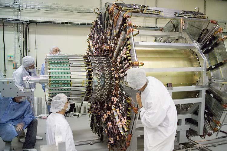
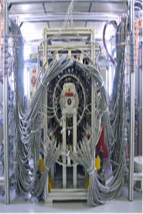
7 Tracking Systems: ATLAS & CMS ATLAS CMS 7
 : B + J/ K + 1 v 1 c 2 2 Primary Vertex d 0 Impact parameter K Secondary Vertex mean path length λ")
8 Primary and secondary vertex Primary and Secondary Decay Vertices Example: B lifetime B ~ 1.6 ps c B = 500 m with Figure of merit: Impact parameter resolution Physics example from LHCb (2010) : B + J/ K + 1 v 1 c 2 2 Primary Vertex d 0 Impact parameter K Secondary Vertex mean path length λ of a meson with b quark or a τ lepton ~ 2 mm fraction visible in transverse plane ~2/3 λ à need sub-mm measurement precision

9 Uncertainty on the transverse impact parameter, d0, depends on the detector radii and space point precisions. Simplified formula for just two layers: r d MS r r r Suggests small r 1, large r 2, small, But precision is degraded by multiple scattering. Example: LHCb (VELO ) (IP)= ( /p T [GeV/c] ) m [PoS VERTEX2010:014,2010.] from Michael Moll

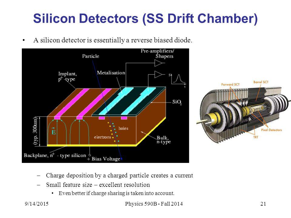
10 Semiconductor detectors Why Si or Ge? Detector production by microelectronic technique leverage progress in integrated circuits technology small dimensions silicon rigidity allows for thin support structure - Moore s Law transistor count doubling every two years


11 Semiconductor Fermi level Pure undoped Si electron density cm 3 Fermi level Maximum electron energy at T = 0 K 300 µm 1 cm 1 cm In this volume there are free charge carriers, but only e-h pairs produced by a M.I.P. ->Reduce number of free charge carriers i.e., deplete the detector Typically make use of reverse biased p-n junctions


")


12 DONOR (N) Doped semiconductor Add elements from V th group, donors, e.g. Arsenic - As. Electrons are the majority carriers. ACCEPTOR (P) Add elements from III rd group, acceptors, e.g. Gallium - Ga Holes are the majority carriers.
13 Doped semiconductor

 region can be made bigger by applying a reverse bias")
14 Doped silicon: P-N Junction PN junction without external voltage Free charges move until the chemical potential is balanced by an electrical potential called the built-in potential The space charge (depletion) region can be made bigger by applying a reverse bias voltage
15 There must be a single Fermi level! Deformation of band structure à potential difference. E p CB n e. V E f VB diffusion of e - into p-zone, h + into n-zone à potential difference stopping diffusion

 where most of the signal is")
16 Silicon Strip Detectors Segmented implant allows to reconstruct the position of the traversing particle in one dimension DC-coupled strip detector simplest position sensitive Silicon detector Standard configuration: Strips p implants Substrate n doped (~2-10 kωcm) and ~300µm thick V dep< 200 V Backside Phosphorous implant to establish ohmic contact and to prevent early breakdown Highest field close to the collecting electrodes (junction side) where most of the signal is induced

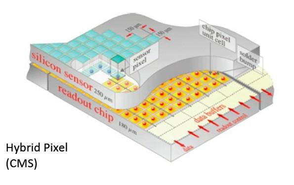
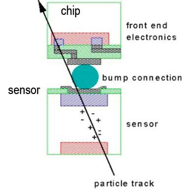
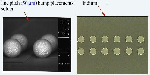
17 Silicon pixel detectors Silicon pixel detectors Segment silicon to diode matrix also readout electronic with same geometry connection by bump bonding techniques detector Flip-chip technique electronics bump bonds RD 19, E. Heijne et al., NIM A 384 (1994) 399
18 Pixel detector Pixel detectors provides space-point information Advantages Small pixel area low detector capacitance ( 1 ff/pixel) large signal-to-noise ratio (e.g. 150:1). Small pixel volume low leakage current ( 1 pa/pixel) Disadvantages Large number of readout channels Large number of electrical connections Large data bandwidth Large power consumption


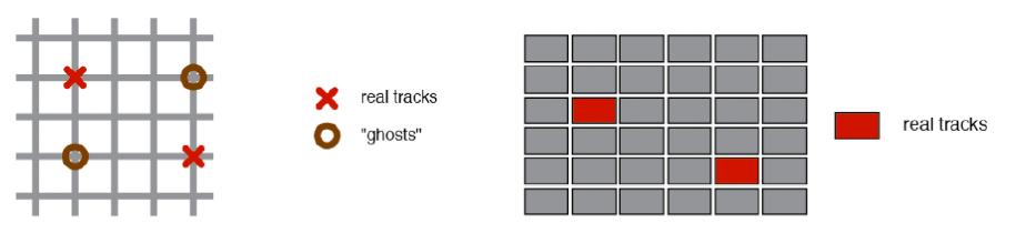
19 Advantages: Double Sided Silicon Detectors More elegant for measuring 2 coordinates than using stereo modules Saves material Disadvantages: Needs special strip insulation of n-side (pstop, p-spray techniques) Complicated manufacturing and handling procedures Expensive Ghost hits possible D. Bortoletto Lecture 4
20 Pixel detector D. Bortoletto Lecture 4 24

21 Signal Most probable charge 0.7 mean Mean charge 25 Bortoletto Lecture 4 D.

22 Diffusion Drift time for: d=300 µm, E=2.5KV/cm: t d (e) = 9 ns, t d (h)=27 ns Diffusion: Typical value: 8 µm for 300 µm drift. Can be exploited to improve position resolution 28 σ D =width root-mean-square of the charge carrier distribution t=drift time K=Boltzman constant e=electron charge D=diffusion coefficient T=temperature µ=mobility µ e = 1350 cm 2 / V s, µ h = 450 cm 2 / V s D. Bortoletto Lecture 4


23 Resolution is the spread One strip clusters Position resolution σ = pitch 12 σ pitch Charge sharing η = PH R PH L + PH R 29


24 Lot of progress on the Pixels! Pixel Layer-2 half shell Pixel ECs at CERN Pixel Layer2, once clamped, inside


25 ATLAS SCT Strip Detector ATLAS Pixel detector CMS Strip Detector
Lecture 18. New gas detectors Solid state trackers
 Lecture 18 New gas detectors Solid state trackers Time projection Chamber Full 3-D track reconstruction x-y from wires and segmented cathode of MWPC z from drift time de/dx information (extra) Drift over
Solid State Detectors Semiconductor detectors Halbleiterdetektoren
 Solid State Detectors Semiconductor detectors Halbleiterdetektoren Doris Eckstein DESY Where are solid state detectors used? > Nuclear Physics: Energy measurement of charged particles (particles up to
Lecture 8. Detectors for Ionizing Particles
 Lecture 8 Detectors for Ionizing Particles Content Introduction Overview of detector systems Sources of radiation Radioactive decay Cosmic Radiation Accelerators Interaction of Radiation with Matter General
Tracking detectors for the LHC. Peter Kluit (NIKHEF)
") Tracking detectors for the LHC Peter Kluit (NIKHEF) Overview lectures part I Principles of gaseous and solid state tracking detectors Tracking detectors at the LHC Drift chambers Silicon detectors Modeling
Tracking detectors for the LHC Peter Kluit (NIKHEF) Overview lectures part I Principles of gaseous and solid state tracking detectors Tracking detectors at the LHC Drift chambers Silicon detectors Modeling
Semiconductor-Detectors
 Semiconductor-Detectors 1 Motivation ~ 195: Discovery that pn-- junctions can be used to detect particles. Semiconductor detectors used for energy measurements ( Germanium) Since ~ 3 years: Semiconductor
Solid State Detectors
 Solid State Detectors Most material is taken from lectures by Michael Moll/CERN and Daniela Bortoletto/Purdue and the book Semiconductor Radiation Detectors by Gerhard Lutz. In gaseous detectors, a charged
Lecture 2. Introduction to semiconductors Structures and characteristics in semiconductors
 Lecture 2 Introduction to semiconductors Structures and characteristics in semiconductors Semiconductor p-n junction Metal Oxide Silicon structure Semiconductor contact Literature Glen F. Knoll, Radiation
Tracking at the LHC. Pippa Wells, CERN
 Tracking at the LHC Aims of central tracking at LHC Some basics influencing detector design Consequences for LHC tracker layout Measuring material before, during and after construction Pippa Wells, CERN
Experimental Methods of Particle Physics
 Experimental Methods of Particle Physics (PHY461) Fall 015 Olaf Steinkamp 36-J- olafs@physik.uzh.ch 044 63 55763 Overview 1) Introduction / motivation measurement of particle momenta: magnetic field early
pp physics, RWTH, WS 2003/04, T.Hebbeker
 3. PP TH 03/04 Accelerators and Detectors 1 pp physics, RWTH, WS 2003/04, T.Hebbeker 2003-12-16 1.2.4. (Inner) tracking and vertexing As we will see, mainly three types of tracking detectors are used:
Instrumentation for Flavor Physics - Lesson I
 Instrumentation for Flavor Physics - Lesson I! Fisica delle Particelle Università di Milano a.a 2013/2014 Outline Lesson I Introduction Basics for detector design Vertex detectors Lesson II Tracking detectors
Lecture 2. Introduction to semiconductors Structures and characteristics in semiconductors
 Lecture 2 Introduction to semiconductors Structures and characteristics in semiconductors Semiconductor p-n junction Metal Oxide Silicon structure Semiconductor contact Literature Glen F. Knoll, Radiation
Radiation Detector 2016/17 (SPA6309)
") Radiation Detector 2016/17 (SPA6309) Semiconductor detectors (Leo, Chapter 10) 2017 Teppei Katori Semiconductor detectors are used in many situations, mostly for some kind of high precision measurement.
Radiation Detector 2016/17 (SPA6309) Semiconductor detectors (Leo, Chapter 10) 2017 Teppei Katori Semiconductor detectors are used in many situations, mostly for some kind of high precision measurement.
The LHC Experiments. TASI Lecture 2 John Conway
 The LHC Experiments TASI 2006 - Lecture 2 John Conway Outline A. Interactions of Particles With Matter B. Tracking Detectors C. Calorimetry D. CMS and ATLAS Design E. The Mystery of Triggering F. Physics
Advantages / Disadvantages of semiconductor detectors
 Advantages / Disadvantages of semiconductor detectors Semiconductor detectors have a high density (compared to gas detector) large energy loss in a short distance diffusion effect is smaller than in gas
Final Examination EE 130 December 16, 1997 Time allotted: 180 minutes
 Final Examination EE 130 December 16, 1997 Time allotted: 180 minutes Problem 1: Semiconductor Fundamentals [30 points] A uniformly doped silicon sample of length 100µm and cross-sectional area 100µm 2
Semiconductor Detectors
 Semiconductor Detectors Summary of Last Lecture Band structure in Solids: Conduction band Conduction band thermal conductivity: E g > 5 ev Valence band Insulator Charge carrier in conductor: e - Charge
etectors for High Energy Physics
 3rd WORKSHOP ON PARTICLE PHYSICS NATIONAL CENTRE FOR PHYSICS (QUAID-I-AZAM UNIVERSITY) etectors for High Energy Physics Lecture II General Detector Concepts Gigi Rolandi Cern Geneva - Switzerland http://rolandi.home.cern.ch/rolandi/
Schottky Rectifiers Zheng Yang (ERF 3017,
 ECE442 Power Semiconductor Devices and Integrated Circuits Schottky Rectifiers Zheng Yang (ERF 3017, email: yangzhen@uic.edu) Power Schottky Rectifier Structure 2 Metal-Semiconductor Contact The work function
Silicon Detectors in High Energy Physics
 Thomas Bergauer (HEPHY Vienna) IPM Teheran 22 May 2011 Sunday: Schedule Silicon Detectors in Semiconductor Basics (45 ) Detector concepts: Pixels and Strips (45 ) Coffee Break Strip Detector Performance
Chap. 11 Semiconductor Diodes
 Chap. 11 Semiconductor Diodes Semiconductor diodes provide the best resolution for energy measurements, silicon based devices are generally used for charged-particles, germanium for photons. Scintillators
ATLAS Pixel Detector Upgrade: The Insertable B-Layer
 UNIVERSITY OF OKLAHOMA GRADUATE COLLEGE HOMER L. DODGE DEPARTMENT OF PHYSICS AND ASTRONOMY ATLAS Pixel Detector Upgrade: The Insertable B-Layer A REPORT SUBMITTED TO THE GRADUATE FACULTY in partial fulfillment
Semiconductor Physics fall 2012 problems
 Semiconductor Physics fall 2012 problems 1. An n-type sample of silicon has a uniform density N D = 10 16 atoms cm -3 of arsenic, and a p-type silicon sample has N A = 10 15 atoms cm -3 of boron. For each
Semiconductor Detectors are Ionization Chambers. Detection volume with electric field Energy deposited positive and negative charge pairs
 1 V. Semiconductor Detectors V.1. Principles Semiconductor Detectors are Ionization Chambers Detection volume with electric field Energy deposited positive and negative charge pairs Charges move in field
Session 6: Solid State Physics. Diode
 Session 6: Solid State Physics Diode 1 Outline A B C D E F G H I J 2 Definitions / Assumptions Homojunction: the junction is between two regions of the same material Heterojunction: the junction is between
Expected Performance of the ATLAS Inner Tracker at the High-Luminosity LHC
 Expected Performance of the ATLAS Inner Tracker at the High-Luminosity LHC Matthias Hamer on behalf of the ATLAS collaboration Introduction The ATLAS Phase II Inner Tracker Expected Tracking Performance
EE 5344 Introduction to MEMS CHAPTER 5 Radiation Sensors
 EE 5344 Introduction to MEMS CHAPTER 5 Radiation Sensors 5. Radiation Microsensors Radiation µ-sensors convert incident radiant signals into standard electrical out put signals. Radiant Signals Classification
CMS Note Mailing address: CMS CERN, CH-1211 GENEVA 23, Switzerland
 Available on CMS information server CMS NOTE 1996/005 The Compact Muon Solenoid Experiment CMS Note Mailing address: CMS CERN, CH-1211 GENEVA 23, Switzerland Performance of the Silicon Detectors for the
Classification of Solids
 Classification of Solids Classification by conductivity, which is related to the band structure: (Filled bands are shown dark; D(E) = Density of states) Class Electron Density Density of States D(E) Examples
Detectors for High Energy Physics
 Detectors for High Energy Physics Ingrid-Maria Gregor, DESY DESY Summer Student Program 2017 Hamburg July 26th/27th Overview I. Detectors for Particle Physics II. Interaction with Matter } Wednesday III.
Spring Semester 2012 Final Exam
 Spring Semester 2012 Final Exam Note: Show your work, underline results, and always show units. Official exam time: 2.0 hours; an extension of at least 1.0 hour will be granted to anyone. Materials parameters
CLASS 12th. Semiconductors
 CLASS 12th Semiconductors 01. Distinction Between Metals, Insulators and Semi-Conductors Metals are good conductors of electricity, insulators do not conduct electricity, while the semiconductors have
Silicon Tracking Detectors for the LHC experiments
 Silicon Tracking Detectors for the LHC experiments Vincenzo Chiochia Physik Institut der Universität Zürich-Irchel CH-8057 Zürich (Switzerland) DESY Seminar March 7 th, 2006 Outline Part 1: 1. Tracking
The ATLAS Silicon Microstrip Tracker
 9th 9th Topical Seminar on Innovative Particle and Radiation Detectors 23-26 May 2004 Siena3 The ATLAS Silicon Microstrip Tracker Zdenek Dolezal, Charles University at Prague, for the ATLAS SCT Collaboration
EECS130 Integrated Circuit Devices
 EECS130 Integrated Circuit Devices Professor Ali Javey 9/18/2007 P Junctions Lecture 1 Reading: Chapter 5 Announcements For THIS WEEK OLY, Prof. Javey's office hours will be held on Tuesday, Sept 18 3:30-4:30
Lecture 12. Semiconductor Detectors - Photodetectors
 Lecture 12 Semiconductor Detectors - Photodetectors Principle of the pn junction photodiode Absorption coefficient and photodiode materials Properties of semiconductor detectors The pin photodiodes Avalanche
PN Junction
 P Junction 2017-05-04 Definition Power Electronics = semiconductor switches are used Analogue amplifier = high power loss 250 200 u x 150 100 u Udc i 50 0 0 50 100 150 200 250 300 350 400 i,u dc i,u u
Status Report: Charge Cloud Explosion
 Status Report: Charge Cloud Explosion J. Becker, D. Eckstein, R. Klanner, G. Steinbrück University of Hamburg Detector laboratory 1. Introduction and Motivation. Set-up available for measurement 3. Measurements
Tracking in High Energy Physics: Silicon Devices!
 Tracking in High Energy Physics: Silicon Devices! G. Leibenguth XIX Graduiertenkolleg Heidelberg 11-12. October 2007 Content Part 1: Basics on semi-conductor Part 2: Construction Part 3: Two Examples Part
Semiconductor X-Ray Detectors. Tobias Eggert Ketek GmbH
 Semiconductor X-Ray Detectors Tobias Eggert Ketek GmbH Semiconductor X-Ray Detectors Part A Principles of Semiconductor Detectors 1. Basic Principles 2. Typical Applications 3. Planar Technology 4. Read-out
Walter Hopkins. February
 B s µ + µ Walter Hopkins Cornell University February 25 2010 Walter Hopkins (Cornell University) Bs µ + µ February 25 2010 1 / 14 Motivation B s µ + µ can only occur through higher order diagrams in Standard
Experimental Particle Physics
 Experimental Particle Physics Particle Interactions and Detectors Lecture 2 17th February 2010 Fergus Wilson, RAL 1/31 How do we detect particles? Particle Types Charged (e - /K - /π - ) Photons (γ) Electromagnetic
Multi wire proportional chamber (MWPC)
") Multi wire proportional chambers Multi wire proportional chamber (MWPC) (G. Charpak et al. 1968, Nobel prize 1992) field lines and equipotentials around anode wires Capacitive coupling of non-screened
Multi wire proportional chambers Multi wire proportional chamber (MWPC) (G. Charpak et al. 1968, Nobel prize 1992) field lines and equipotentials around anode wires Capacitive coupling of non-screened
ECE 340 Lecture 27 : Junction Capacitance Class Outline:
 ECE 340 Lecture 27 : Junction Capacitance Class Outline: Breakdown Review Junction Capacitance Things you should know when you leave M.J. Gilbert ECE 340 Lecture 27 10/24/11 Key Questions What types of
Development of Radiation Hard Si Detectors
 Development of Radiation Hard Si Detectors Dr. Ajay K. Srivastava On behalf of Detector Laboratory of the Institute for Experimental Physics University of Hamburg, D-22761, Germany. Ajay K. Srivastava
Nuclear and Particle Physics 4b Physics of the Quark Gluon Plasma
 Nuclear and Particle Physics 4b Physics of the Quark Gluon Plasma Goethe University Frankfurt GSI Helmholtzzentrum für Schwerionenforschung Lectures and Exercise Summer Semester 2016 1 Organization Language:
Lecture 2. Introduction to semiconductors Structures and characteristics in semiconductors. Fabrication of semiconductor sensor
 Lecture 2 Introduction to semiconductors Structures and characteristics in semiconductors Semiconductor p-n junction Metal Oxide Silicon structure Semiconductor contact Fabrication of semiconductor sensor
A-Exam: The Rare B s µ + µ decay and tanβ
 A-Exam: The Rare B s µ + µ decay and tanβ Walter Hopkins Physics Department, Cornell University. The rare B decay of B s µ + µ is a promising decay channel to find beyond the Standard Model (BSM) physics
Outline, measurement of position
 Outline, measurement of position Proportional and drift chambers: issues: field shape, geometry of the chamber, gas mixture, gas gain, resolution, drift velocity and drift time, Lorentz angle. Cathode
L03: pn Junctions, Diodes
 8/30/2012 Page 1 of 5 Reference:C:\Users\Bernhard Boser\Documents\Files\Lib\MathCAD\Default\defaults.mcd L03: pn Junctions, Diodes Intrinsic Si Q: What are n, p? Q: Is the Si charged? Q: How could we make
Semiconductor Physics fall 2012 problems
 Semiconductor Physics fall 2012 problems 1. An n-type sample of silicon has a uniform density N D = 10 16 atoms cm -3 of arsenic, and a p-type silicon sample has N A = 10 15 atoms cm -3 of boron. For each
Study of Edgeless TimePix Pixel Devices. Dylan Hsu Syracuse University 4/30/2014
 Study of Edgeless TimePix Pixel Devices Dylan Syracuse University 2 3 Million-Dollar Question Universe is made of matter Particle decays putatively produce equal amounts of matter and antimatter Where
Experimental Particle Physics
 Experimental Particle Physics Particle Interactions and Detectors Lecture 2 2nd May 2014 Fergus Wilson, RAL 1/31 How do we detect particles? Particle Types Charged (e - /K - /π - ) Photons (γ) Electromagnetic
Peter Fischer, ziti, Universität Heidelberg. Silicon Detectors & Readout Electronics
 Silicon Detectors and Readout Electronics Peter Fischer, ziti, Universität Heidelberg 1 Content of the Lecture (sorted by subject) Introduction: Applications of silicon detectors Requirements, measured
OPTI510R: Photonics. Khanh Kieu College of Optical Sciences, University of Arizona Meinel building R.626
 OPTI510R: Photonics Khanh Kieu College of Optical Sciences, University of Arizona kkieu@optics.arizona.edu Meinel building R.626 Announcements Homework #6 is assigned, due May 1 st Final exam May 8, 10:30-12:30pm
Semiconductor Physics Problems 2015
 Semiconductor Physics Problems 2015 Page and figure numbers refer to Semiconductor Devices Physics and Technology, 3rd edition, by SM Sze and M-K Lee 1. The purest semiconductor crystals it is possible
Silicon Detectors in High Energy Physics
 Thomas Bergauer (HEPHY Vienna) IPM Teheran 22 May 2011 Sunday: Schedule Semiconductor Basics (45 ) Silicon Detectors in Detector concepts: Pixels and Strips (45 ) Coffee Break Strip Detector Performance
n N D n p = n i p N A
 Summary of electron and hole concentration in semiconductors Intrinsic semiconductor: E G n kt i = pi = N e 2 0 Donor-doped semiconductor: n N D where N D is the concentration of donor impurity Acceptor-doped
Risultati dell esperimento ATLAS dopo il run 1 di LHC. C. Gemme (INFN Genova), F. Parodi (INFN/University Genova) Genova, 28 Maggio 2013
, F. Parodi (INFN/University Genova) Genova, 28 Maggio 2013") Risultati dell esperimento ATLAS dopo il run 1 di LHC C. Gemme (INFN Genova), F. Parodi (INFN/University Genova) Genova, 28 Maggio 2013 1 LHC physics Standard Model is a gauge theory based on the following
Risultati dell esperimento ATLAS dopo il run 1 di LHC C. Gemme (INFN Genova), F. Parodi (INFN/University Genova) Genova, 28 Maggio 2013 1 LHC physics Standard Model is a gauge theory based on the following
Section 12: Intro to Devices
 Section 12: Intro to Devices Extensive reading materials on reserve, including Robert F. Pierret, Semiconductor Device Fundamentals Bond Model of Electrons and Holes Si Si Si Si Si Si Si Si Si Silicon
Gabriele Simi Università di Padova
 From the pn junction to the particle detector Gabriele Simi Università di Padova Scuola Nazionale "Rivelatori ed Elettronica per Fisica delle Alte Energie, Astrofisica, Applicazioni Spaziali e Fisica Medica"
Energetic particles and their detection in situ (particle detectors) Part II. George Gloeckler
 Part II. George Gloeckler") Energetic particles and their detection in situ (particle detectors) Part II George Gloeckler University of Michigan, Ann Arbor, MI University of Maryland, College Park, MD Simple particle detectors Gas-filled
Energetic particles and their detection in situ (particle detectors) Part II George Gloeckler University of Michigan, Ann Arbor, MI University of Maryland, College Park, MD Simple particle detectors Gas-filled
PHY492: Nuclear & Particle Physics. Lecture 25. Particle Detectors
 PHY492: Nuclear & Particle Physics Lecture 25 Particle Detectors http://pdg.lbl.gov/2006/reviews/contents_sports.html S(T ) = dt dx nz = ρa 0 Units for energy loss Minimum ionization in thin solids Z/A
Consider a uniformly doped PN junction, in which one region of the semiconductor is uniformly doped with acceptor atoms and the adjacent region is
 CHAPTER 7 The PN Junction Consider a uniformly doped PN junction, in which one region of the semiconductor is uniformly doped with acceptor atoms and the adjacent region is uniformly doped with donor atoms.
Identifying Particle Trajectories in CMS using the Long Barrel Geometry
 Identifying Particle Trajectories in CMS using the Long Barrel Geometry Angela Galvez 2010 NSF/REU Program Physics Department, University of Notre Dame Advisor: Kevin Lannon Abstract The Compact Muon Solenoid
LEC E T C U T R U E R E 17 -Photodetectors
 LECTURE 17 -Photodetectors Topics to be covered Photodetectors PIN photodiode Avalanche Photodiode Photodetectors Principle of the p-n junction Photodiode A generic photodiode. Photodetectors Principle
Junction Diodes. Tim Sumner, Imperial College, Rm: 1009, x /18/2006
 Junction Diodes Most elementary solid state junction electronic devices. They conduct in one direction (almost correct). Useful when one converts from AC to DC (rectifier). But today diodes have a wide
Alignment of the ATLAS Inner Detector Tracking System
 Alignment of the ATLAS Inner Detector Tracking System Department of Physics and Astronomy, University of Pennsylvania E-mail: johnda@hep.upenn.edu These proceedings present the track-based method of aligning
Introduction to Silicon Detectors. G.Villani STFC Rutherford Appleton Laboratory Particle Physics Department
 Introduction to Silicon Detectors G.Villani STFC Rutherford Appleton Laboratory Particle Physics Department 1 Outlook Introduction to physics of Si and detection Examples of detectors Radiation effects
Surfaces, Interfaces, and Layered Devices
 Surfaces, Interfaces, and Layered Devices Building blocks for nanodevices! W. Pauli: God made solids, but surfaces were the work of Devil. Surfaces and Interfaces 1 Interface between a crystal and vacuum
Dario Barberis Evaluation of GEANT4 Electromagnetic and Hadronic Physics in ATLAS
 Dario Barberis Evaluation of GEANT4 Electromagnetic and Hadronic Physics in ATLAS LC Workshop, CERN, 15 Nov 2001 Dario Barberis Genova University/INFN 1 The ATLAS detector LC Workshop, CERN, 15 Nov 2001
Detectors & Beams. Giuliano Franchetti and Alberica Toia Goethe University Frankfurt GSI Helmholtzzentrum für Schwerionenforschung
 Detectors & Beams Giuliano Franchetti and Alberica Toia Goethe University Frankfurt GSI Helmholtzzentrum für Schwerionenforschung Pro-seminar Winter Semester 2015-16 DPG Spring Meeting Giuliano Franchetti
Chapter 7. The pn Junction
 Chapter 7 The pn Junction Chapter 7 PN Junction PN junction can be fabricated by implanting or diffusing donors into a P-type substrate such that a layer of semiconductor is converted into N type. Converting
Section 12: Intro to Devices
 Section 12: Intro to Devices Extensive reading materials on reserve, including Robert F. Pierret, Semiconductor Device Fundamentals EE143 Ali Javey Bond Model of Electrons and Holes Si Si Si Si Si Si Si
Photosynthesis & Solar Power Harvesting
 Lecture 23 Semiconductor Detectors - Photodetectors Principle of the pn junction photodiode Absorption coefficient and photodiode materials Properties of semiconductor detectors The pin photodiodes Avalanche
Interaction of particles in matter
 Interaction of particles in matter Particle lifetime : N(t) = e -t/ Particles we detect ( > 10-10 s, c > 0.03m) Charged particles e ± (stable m=0.511 MeV) μ ± (c = 659m m=0.102 GeV) ± (c = 7.8m m=0.139
1st Year-Computer Communication Engineering-RUC. 4- P-N Junction
 4- P-N Junction We begin our study of semiconductor devices with the junction for three reasons. (1) The device finds application in many electronic systems, e.g., in adapters that charge the batteries
1 Name: Student number: DEPARTMENT OF PHYSICS AND PHYSICAL OCEANOGRAPHY MEMORIAL UNIVERSITY OF NEWFOUNDLAND. Fall :00-11:00
 1 Name: DEPARTMENT OF PHYSICS AND PHYSICAL OCEANOGRAPHY MEMORIAL UNIVERSITY OF NEWFOUNDLAND Final Exam Physics 3000 December 11, 2012 Fall 2012 9:00-11:00 INSTRUCTIONS: 1. Answer all seven (7) questions.
Ranjeet Dalal, Ashutosh Bhardwaj, Kirti Ranjan, Kavita Lalwani and Geetika Jain
 Simulation of Irradiated Si Detectors, Ashutosh Bhardwaj, Kirti Ranjan, Kavita Lalwani and Geetika Jain CDRST, Department of physics and Astrophysics, University of Delhi, India E-mail: rdalal@cern.ch
CMS Note Mailing address: CMS CERN, CH-1211 GENEVA 23, Switzerland
 Available on CMS information server CMS NOTE 21/17 The Compact Muon Solenoid Experiment CMS Note Mailing address: CMS CERN, CH-1211 GENEVA 23, Switzerland 2 March 21 Study of a Level-3 Tau Trigger with
ELEN0037 Microelectronic IC Design. Prof. Dr. Michael Kraft
 ELEN0037 Microelectronic IC Design Prof. Dr. Michael Kraft Lecture 2: Technological Aspects Technology Passive components Active components CMOS Process Basic Layout Scaling CMOS Technology Integrated
LHC. Jim Bensinger Brandeis University New England Particle Physics Student Retreat August 26, 2004
 Experiments @ LHC Jim Bensinger Brandeis University New England Particle Physics Student Retreat August 26, 2004 Outline of Presentation Existing Spectrometers A Certain Sameness The Basic Interaction
Review of Semiconductor Fundamentals
 ECE 541/ME 541 Microelectronic Fabrication Techniques Review of Semiconductor Fundamentals Zheng Yang (ERF 3017, email: yangzhen@uic.edu) Page 1 Semiconductor A semiconductor is an almost insulating material,
SILICON PARTICLE DETECTOR
 SILICON PARTICLE DETECTOR Supervised Learning Project Eslikumar Adiandhra 12D260012 Department of Physics, IIT Bombay Guide: Prof. Raghava Varma Department of Physics, IIT Bombay November 8, 2015 Abstract
Review of Semiconductor Drift Detectors
 Pavia October 25, 2004 Review of Semiconductor Drift Detectors Talk given by Pavel Rehak following a presentation on 5 th Hiroshima Symposium of Semiconductor Tracking Detectors Outline of the Review Principles
Recent CMS results on heavy quarks and hadrons. Alice Bean Univ. of Kansas for the CMS Collaboration
 Recent CMS results on heavy quarks and hadrons Alice Bean Univ. of Kansas for the CMS Collaboration July 25, 2013 Outline CMS at the Large Hadron Collider Cross section measurements Search for state decaying
ESE 372 / Spring 2013 / Lecture 5 Metal Oxide Semiconductor Field Effect Transistor
 Metal Oxide Semiconductor Field Effect Transistor V G V G 1 Metal Oxide Semiconductor Field Effect Transistor We will need to understand how this current flows through Si What is electric current? 2 Back
Some studies for ALICE
 Some studies for ALICE Motivations for a p-p programme in ALICE Special features of the ALICE detector Preliminary studies of Physics Performances of ALICE for the measurement of some global properties
For the following statements, mark ( ) for true statement and (X) for wrong statement and correct it.
 for true statement and (X) for wrong statement and correct it.") Benha University Faculty of Engineering Shoubra Electrical Engineering Department First Year communications. Answer all the following questions Illustrate your answers with sketches when necessary. The
Benha University Faculty of Engineering Shoubra Electrical Engineering Department First Year communications. Answer all the following questions Illustrate your answers with sketches when necessary. The
Digital Calorimetry for Future Linear Colliders. Tony Price University of Birmingham University of Birmingham PPE Seminar 13 th November 2013
 Digital Calorimetry for Future Linear Colliders Tony Price University of Birmingham University of Birmingham PPE Seminar 13 th November 2013 Overview The ILC Digital Calorimetry The TPAC Sensor Electromagnetic
Chapter 4. Photodetectors
 Chapter 4 Photodetectors Types of photodetectors: Photoconductos Photovoltaic Photodiodes Avalanche photodiodes (APDs) Resonant-cavity photodiodes MSM detectors In telecom we mainly use PINs and APDs.
Commissioning of the ATLAS LAr Calorimeter
 Commissioning of the ATLAS LAr Calorimeter S. Laplace (CNRS/LAPP) on behalf of the ATLAS Liquid Argon Calorimeter Group Outline: ATLAS in-situ commissioning steps Introduction to the ATLAS LAr Calorimeter
ECE 335: Electronic Engineering Lecture 2: Semiconductors
 Faculty of Engineering ECE 335: Electronic Engineering Lecture 2: Semiconductors Agenda Intrinsic Semiconductors Extrinsic Semiconductors N-type P-type Carrier Transport Drift Diffusion Semiconductors
Silicon Detectors. Particle Physics
 Mitglied der Helmholtz-Gemeinschaft Silicon Detectors for Particle Physics 9. August 2012 Ralf Schleichert, Institut für Kernphysik Outline Different Cameras Silicon Detectors Taking Pictures in Particle
4. LHC experiments Marcello Barisonzi LHC experiments August
 4. LHC experiments 1 Summary from yesterday: Hadron colliders play an important role in particle physics discory but also precision measurements LHC will open up TeV energy range new particles with 3-5
The ATLAS Detector - Inside Out Julia I. Hofmann
 The ATLAS Detector - Inside Out Julia I. Hofmann KIP Heidelberg University Outline: 1st lecture: The Detector 2nd lecture: The Trigger 3rd lecture: The Analysis (mine) Motivation Physics Goals: Study Standard
Impact of high photon densities on AGIPD requirements
 Impact of high photon densities on AGIPD requirements Julian Becker University of Hamburg Detector Laboratory new data 1. Heating estimations 2. Confined breakdown 3. Range switching in adjacent pixels
Electronics EC /2/2012. * In-class exams: 40% 7 th week exam 25% 12 th week exam 15%
 Arab Academy for Science, Technology and Maritime Transport Electronics EC 331 Dr. Mohamed Hassan Course Assessment * In-class exams: 40% 7 th week exam 25% 12 th week exam 15% *Tutorial exams and activities:
The ATLAS C. Gemme, F.Parodi
 The ATLAS Experiment@LHC C. Gemme, F.Parodi LHC physics test the Standard Model, hopefully find physics beyond SM find clues to the EWK symmetry breaking - Higgs(ses)? Standard Model is a gauge theory
Lecture 15 - The pn Junction Diode (I) I-V Characteristics. November 1, 2005
 I-V Characteristics. November 1, 2005") 6.012 - Microelectronic Devices and Circuits - Fall 2005 Lecture 15-1 Lecture 15 - The pn Junction Diode (I) I-V Characteristics November 1, 2005 Contents: 1. pn junction under bias 2. I-V characteristics
6.012 - Microelectronic Devices and Circuits - Fall 2005 Lecture 15-1 Lecture 15 - The pn Junction Diode (I) I-V Characteristics November 1, 2005 Contents: 1. pn junction under bias 2. I-V characteristics