KATIHAL FİZİĞİ MNT-510
|
|
|
- Beatrice Della McDowell
- 5 years ago
- Views:
Transcription
1 KATIHAL FİZİĞİ MNT-510 YARIİLETKENLER Kaynaklar: Katıhal Fiziği, Prof. Dr. Mustafa Dikici, Seçkin Yayıncılık Katıhal Fiziği, Şakir Aydoğan, Nobel Yayıncılık, Physics for Computer Science Students: With Emphasis on Atomic and Semiconductor Physics, Narciso Garcia, Arthur Damask, Steven Schwarz, Springer Lecture Notes, Prof. A. Niknejad, University of California, Berkley
2 The highest energy band completely filled with electrons (at T = 0 K) is called the Valence Band The next band is called the Conduction Band The energy difference between the bottom of the Conduction and the top of the Valence bands is called the Band Gap
3 Conduction Electron Conduction is easy to imagine: electrons (in the conduction band) move almost like free particles Hole Conduction is due to positively charged particles in the valence band

4 Intrinsic Semiconductors Consider nominally pure semiconductor at T = 0 K There is no electrons in the conduction band At T > 0 K a small fraction of electrons is thermally excited into the conduction band, leaving the same number of holes in the valence band
5 Intrinsic Semiconductors at T >0 K Electrons and holes contribute to the current when a voltage is applied


6 Carrier Concentrations at T >0 K Let s take E V = 0, then E C = E G The number of electrons equals the number of holes, n e = n h The Fermi level lies in the middle of the band gap n e = n h increase rapidly with temperature

7 Carrier Concentrations E G of selected semiconductors Si: 1.1eV Ge: 0.7eV GaAs: 1.4eV ZnSe: 2.7eV Carrier effective masses for selected semiconductors GaAs: m e* = 0.067m 0 ; m h* = 0.45m 0 Si: m e * = 0.26m 0 ; m h * = 0.49m 0 Ge: m e * = 0.04m 0 ; m h * = 0.28m 0 ZnSe: m e * = 0.21m 0 ; m h * = 0.74m 0 Carrier concentration falls with 1/T, i.e. increase with T
8 Doping Semiconductors can be easily doped Doping is the incorporation of [substitutional] impurities into a semiconductor according to our requirements In other words, impurities are introduced in a controlled manner Impurities change the conductivity of the material so that it can be fabricated into a device
9 Extrinsic Semiconductors Electrical Properties of Semiconductors can be altered drastically by adding minute amounts of suitable impurities to the pure crystals Impurities: Atoms of the elements different from those forming solid Interstitial: foreign atoms squeezed between regular sites crystal sites Substitutional: foreign atoms occupying the sites of host atoms
10 Donors We use Silicon (Si) as an example Substitute one Si (Group IV) atom with a Group V atom (e.g. As or P) Si atoms have four valence electrons that participate in covalent bonding When a Group V atom replaces a Si atom, it will use four of its electrons to form the covalent bonding What happens with the remaining electron?
11 Donors The remaining electron will not be very tightly bound, and can be easily ionized at T > 0K Ionized electron is free to conduct In term of the band structure, this electron is now in the conduction band Such Group V impurities are called Donors, since they donate electrons into the Conduction Band Semiconductors doped by donors are called n-type semiconductors
12 Donors: Energy Levels The Band Structure View Such impurities create an energy level within the band gap, close to the conduction band A donor is similar to a hydrogen atom A positive charge with a single electron within its potential Such impurities are called hydrogenic donors They create so-called shallow levels - the levels that are very close to the conduction band, so the energy required to ionize the atom is small and a sizable fraction of donor atoms will be ionized at room temperature
13
14
15 This crystal has been doped with a pentavalent impurity. The free electrons in n type silicon support the flow of current.
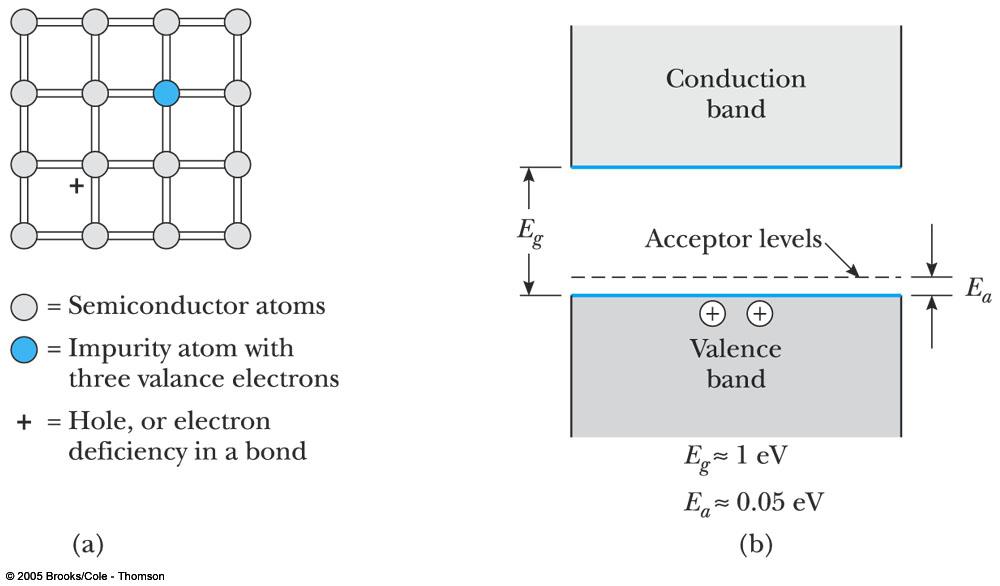
16 Acceptors Use Silicon (Si) as an example Substitute one Group III atom (e.g. Al or In) with a Si (Group IV) atom Si atoms have four valence electrons that participate in the covalent bonding When a Group III atom replaces a Si atom, it cannot complete a tetravalent bond scheme An electronic vacancy hole is formed when an electron from the valence band is grabbed by the atom so that the core is negatively charged, the hole created is then attracted the negative core At T = 0 K this hole stays with atom localized hole At T > 0 K, electron from the neighboring Si atom can jump into this hole the hole can then migrate and contribute to the current


17 Acceptors At T > 0 K, electron from the neighboring Si atom can jump into this hole the hole starts to migrate, contributing to the current We can say that this impurity atom accepted an electron, so we call them Acceptors Acceptors accept electrons, but donate free holes
18 Acceptors By incorporating the electron into the impurity atom we can represent this (T = 0 K) as a negative charge in the core with a positive charge (hole) outside the core attracted by its [Coulomb] potential At T > 0 K this hole can be ionized Such semiconductors are called p-type semiconductors since they contribute positive charge carriers
19 Acceptor: Energy Levels From the Band Structure View Such impurities create energy levels within the band gap, close to the valence band They are similar to negative hydrogen atoms Such impurities are called hydrogenic acceptors They create shallow levels - levels that are very close to the valence band, so the energy required to ionize the atom (accept the electron that fills the hole and creates another hole further from the substituted atom) is small
20
21 This crystal has been doped with a trivalent impurity. The holes in p type silicon contribute to the current. Note that the hole current direction is opposite to electron current so the electrical current is in the same direction
22
23 Carrier Concentrations in Extrinsic Semiconductors The carrier densities in extrinsic semiconductors can be very high It depends on doping levels ([net] dopant concentration) and ionization energy of the dopants Often both types of impurities are present If the total concentration of donors (N D ) is larger than the total concentration of acceptors (N A ) have an n-type semiconductor In the opposite case have a p-type semiconductor
24 Charge Neutrality Equation To calculate the charge concentration, the charge neutrality condition is used, since the net charge in a uniformly doped semiconductor is zero Otherwise, there will be a net flow of charge from one point to another resulting in current flow p is the concentration of holes in the valence band n is the electron concentration N D is the ionized donor concentration N A - is the ionized acceptor concentration
25 Resistivity of Semiconductors The carrier concentration and thus the conductivity is dominated by its essentially exponential dependence on temperature For intrinsic semiconductors For impurity semiconductors E F is first between the impurity level and the band edge and then approaches E g /2 after most of the impurities are ionized
26 Optical Properties If semiconductor or insulator does not have many impurity levels in the band gap, photons with energies smaller than the band gap energy can t be absorbed There are no quantum states with energies in the band gap This explains why many insulators or wide band gap semiconductors are transparent to visible light, whereas narrow band semiconductors (Si, GaAs) are not

27 Optical Properties Some applications Emission: light emitting diode (LED) and Laser Diode (LD) Absorption: Filtering Sunglasses Si filters: transmission of infra red light with simultaneous blocking of visible light

28 Optical Properties If there are many impurity levels the photons with energies smaller than the band gap energy can be absorbed, by exciting electrons or holes from these energy levels into the conduction or valence band, respectively Example: Colored Diamonds
29 Photoconductivity Charge carriers (electrons or holes or both) created in the corresponding bands by absorbed light can also participate in current flow, and thus should increase the current for a given applied voltage, i.e., the conductivity increases This effect is called Photoconductivity
30 Photoconductivity Important Applications (Garcia 26.6) Night vision systems imaging IR radiation Solar cells Radiation detectors Photoelectric cells (e.g., used for automatic doors) Xerography CCD ( Digital Cameras )
31 PN Junctions: Overview The most important device is a junction between a p-type region and an n-type region When the junction is first formed, due to the concentration gradient, mobile charges transfer near junction Electrons leave n-type region and holes leave p-type region These mobile carriers become minority carriers in new region (can t penetrate far due to recombination) Due to charge transfer, a voltage difference occurs between regions This creates a field at the junction that causes drift currents to oppose the diffusion current In thermal equilibrium, drift current and diffusion must balance p-type N A N D n-type V
32 Diffusion Diffusion occurs when there exists a concentration gradient In the figure below, imagine that we fill the left chamber with a gas at temperate T If we suddenly remove the divider, what happens? The gas will fill the entire volume of the new chamber. How does this occur?
33 Diffusion (cont) The net motion of gas molecules to the right chamber was due to the concentration gradient If each particle moves on average left or right then eventually half will be in the right chamber If the molecules were charged (or electrons), then there would be a net current flow The diffusion current flows from high concentration to low concentration:
34 Total Current and Boundary Conditions When both drift and diffusion are present, the total current is given by the sum: In resistors, the carrier is approximately uniform and the second term is nearly zero For currents flowing uniformly through an interface (no charge accumulation), the field is discontinous
35 Carrier Concentration and Potential In thermal equilibrium, there are no external fields and we thus expect the electron and hole current densities to be zero:
36 Carrier Concentration and Potential (2) We have an equation relating the potential to the carrier concentration If we integrate the above equation we have We define the potential reference to be intrinsic Si:
37 Carrier Concentration Versus Potential The carrier concentration is thus a function of potential Check that for zero potential, we have intrinsic carrier concentration (reference). If we do a similar calculation for holes, we arrive at a similar equation Note that the law of mass action is upheld
38 The Doping Changes Potential Due to the log nature of the potential, the potential changes linearly for exponential increase in doping: Quick calculation aid: For a p-type concentration of cm -3, the potential is -360 mv N-type materials have a positive potential with respect to intrinsic Si
39 PN Junction Currents Consider the PN junction in thermal equilibrium Again, the currents have to be zero, so we have
40 PN Junction Fields p-type n-type N A N D Transition Region
41 Total Charge in Transition Region To solve for the electric fields, we need to write down the charge density in the transition region: In the p-side of the junction, there are very few electrons and only acceptors: Since the hole concentration is decreasing on the p-side, the net charge is negative:
42 Charge on N-Side Analogous to the p-side, the charge on the n-side is given by: The net charge here is positive since: Transition Region
43 Exact Solution for Fields Given the above approximations, we now have an expression for the charge density We also have the following result from electrostatics Notice that the potential appears on both sides of the equation difficult problem to solve A much simpler way to solve the problem
44 Depletion Approximation Let s assume that the transition region is completely depleted of free carriers (only immobile dopants exist) Then the charge density is given by The solution for electric field is now easy Field zero outside transition region
45 Depletion Approximation (2) Since charge density is a constant If we start from the n-side we get the following result Field zero outside transition region
46 Plot of Fields In Depletion Region p-type N A Depletion Region n-type N D E-Field zero outside of depletion region Note the asymmetrical depletion widths
47 Continuity of E-Field Across Junction Recall that E-Field diverges on charge. For a sheet charge at the interface, the E-field could be discontinuous In our case, the depletion region is only populated by a background density of fixed charges so the E-Field is continuous What does this imply? Total fixed charge in n-region equals fixed charge in p-region! Somewhat obvious result.
48 Potential Across Junction From our earlier calculation we know that the potential in the n-region is higher than p-region The potential has to smoothly transition form high to low in crossing the junction Physically, the potential difference is due to the charge transfer that occurs due to the concentration gradient Let s integrate the field to get the potential:
49 Potential Across Junction We arrive at potential on p-side (parabolic) Do integral on n-side Potential must be continuous at interface (field finite at interface)
50 Solve for Depletion Lengths We have two equations and two unknowns. We are finally in a position to solve for the depletion depths (1) (2)
51 Sanity Check Does the above equation make sense? Let s say we dope one side very highly. Then physically we expect the depletion region width for the heavily doped side to approach zero: Entire depletion width dropped across p-region
52 Total Depletion Width The sum of the depletion widths is the space charge region This region is essentially depleted of all mobile charge Due to high electric field, carriers move across region at velocity saturated speed
53 Have we invented a battery? Can we harness the PN junction and turn it into a battery?? Numerical example:
54 Contact Potential The contact between a PN junction creates a potential difference Likewise, the contact between two dissimilar metals creates a potential difference (proportional to the difference between the work functions) When a metal semiconductor junction is formed, a contact potential forms as well If we short a PN junction, the sum of the voltages around the loop must be zero: n p
55 Diode under Thermal Equilibrium Minority Carrier Close to Thermal Junction Generation p-type n-type Carrier with energy Recombination below barrier height Diffusion small since few carriers have enough energy to penetrate barrier Drift current is small since minority carriers are few and far between: Only minority carriers generated within a diffusion length can contribute current Important Point: Minority drift current independent of barrier! Diffusion current strong (exponential) function of barrier
56 Reverse Bias Reverse Bias causes an increases barrier to diffusion Diffusion current is reduced exponentially p-type n-type Drift current does not change Net result: Small reverse current
57 Forward Bias Forward bias causes an exponential increase in the number of carriers with sufficient energy to penetrate barrier Diffusion current increases exponentially p-type n-type Drift current does not change Net result: Large forward current
58 Diode I-V Curve Diode IV relation is an exponential function This exponential is due to the Boltzmann distribution of carriers versus energy For reverse bias the current saturations to the drift current due to minority carriers
59 Minority Carriers at Junction Edges Minority carrier concentration at boundaries of depletion region increase as barrier lowers the function is (minority) hole conc. on n-side of barrier (majority) hole conc. on p-side of barrier (Boltzmann s Law)
60 Law of the Junction Minority carrier concentrations at the edges of the depletion region are given by: Note 1: N A and N D are the majority carrier concentrations on the other side of the junction Note 2: we can reduce these equations further by substituting V D = 0 V (thermal equilibrium) Note 3: assumption that p n << N D and n p << N A
61 Minority Carrier Concentration Minority Carrier Diffusion Length The minority carrier concentration in the bulk region for forward bias is a decaying exponential due to recombination
62 Steady-State Concentrations Assume that none of the diffusing holes and electrons recombine get straight lines This also happens if the minority carrier diffusion lengths are much larger than W n,p
63 Diode Current Densities
64 Diode Circuits Rectifier (AC to DC conversion) Average value circuit Peak detector (AM demodulator) DC restorer Voltage doubler / quadrupler /
n N D n p = n i p N A
 Summary of electron and hole concentration in semiconductors Intrinsic semiconductor: E G n kt i = pi = N e 2 0 Donor-doped semiconductor: n N D where N D is the concentration of donor impurity Acceptor-doped
Lecture 2. Semiconductor Physics. Sunday 4/10/2015 Semiconductor Physics 1-1
 Lecture 2 Semiconductor Physics Sunday 4/10/2015 Semiconductor Physics 1-1 Outline Intrinsic bond model: electrons and holes Charge carrier generation and recombination Intrinsic semiconductor Doping:
Engineering 2000 Chapter 8 Semiconductors. ENG2000: R.I. Hornsey Semi: 1
 Engineering 2000 Chapter 8 Semiconductors ENG2000: R.I. Hornsey Semi: 1 Overview We need to know the electrical properties of Si To do this, we must also draw on some of the physical properties and we
Unit IV Semiconductors Engineering Physics
 Introduction A semiconductor is a material that has a resistivity lies between that of a conductor and an insulator. The conductivity of a semiconductor material can be varied under an external electrical
Chapter 1 Overview of Semiconductor Materials and Physics
 Chapter 1 Overview of Semiconductor Materials and Physics Professor Paul K. Chu Conductivity / Resistivity of Insulators, Semiconductors, and Conductors Semiconductor Elements Period II III IV V VI 2 B
Chemistry Instrumental Analysis Lecture 8. Chem 4631
 Chemistry 4631 Instrumental Analysis Lecture 8 UV to IR Components of Optical Basic components of spectroscopic instruments: stable source of radiant energy transparent container to hold sample device
EE 446/646 Photovoltaic Devices I. Y. Baghzouz
 EE 446/646 Photovoltaic Devices I Y. Baghzouz What is Photovoltaics? First used in about 1890, the word has two parts: photo, derived from the Greek word for light, volt, relating to electricity pioneer
electronics fundamentals
 electronics fundamentals circuits, devices, and applications THOMAS L. FLOYD DAVID M. BUCHLA Lesson 1: Diodes and Applications Semiconductors Figure 1-1 The Bohr model of an atom showing electrons in orbits
CLASS 12th. Semiconductors
 CLASS 12th Semiconductors 01. Distinction Between Metals, Insulators and Semi-Conductors Metals are good conductors of electricity, insulators do not conduct electricity, while the semiconductors have
Lecture 15: Optoelectronic devices: Introduction
 Lecture 15: Optoelectronic devices: Introduction Contents 1 Optical absorption 1 1.1 Absorption coefficient....................... 2 2 Optical recombination 5 3 Recombination and carrier lifetime 6 3.1
Lecture 2. Introduction to semiconductors Structures and characteristics in semiconductors
 Lecture 2 Introduction to semiconductors Structures and characteristics in semiconductors Semiconductor p-n junction Metal Oxide Silicon structure Semiconductor contact Literature Glen F. Knoll, Radiation
Electronic PRINCIPLES
 MALVINO & BATES Electronic PRINCIPLES SEVENTH EDITION Chapter 2 Semiconductors Topics Covered in Chapter 2 Conductors Semiconductors Silicon crystals Intrinsic semiconductors Two types of flow Doping a
Diodes. anode. cathode. cut-off. Can be approximated by a piecewise-linear-like characteristic. Lecture 9-1
 Diodes mplest nonlinear circuit element Basic operation sets the foundation for Bipolar Junction Transistors (BJTs) Also present in Field Effect Transistors (FETs) Ideal diode characteristic anode cathode
Electro - Principles I
 Electro - Principles I Page 10-1 Atomic Theory It is necessary to know what goes on at the atomic level of a semiconductor so the characteristics of the semiconductor can be understood. In many cases a
ELECTRONIC DEVICES AND CIRCUITS SUMMARY
 ELECTRONIC DEVICES AND CIRCUITS SUMMARY Classification of Materials: Insulator: An insulator is a material that offers a very low level (or negligible) of conductivity when voltage is applied. Eg: Paper,
The photovoltaic effect occurs in semiconductors where there are distinct valence and
 How a Photovoltaic Cell Works The photovoltaic effect occurs in semiconductors where there are distinct valence and conduction bands. (There are energies at which electrons can not exist within the solid)
Charge Carriers in Semiconductor
 Charge Carriers in Semiconductor To understand PN junction s IV characteristics, it is important to understand charge carriers behavior in solids, how to modify carrier densities, and different mechanisms
Electronic Circuits for Mechatronics ELCT 609 Lecture 2: PN Junctions (1)
") Electronic Circuits for Mechatronics ELCT 609 Lecture 2: PN Junctions (1) Assistant Professor Office: C3.315 E-mail: eman.azab@guc.edu.eg 1 Electronic (Semiconductor) Devices P-N Junctions (Diodes): Physical
Electronic Circuits for Mechatronics ELCT 609 Lecture 2: PN Junctions (1) Assistant Professor Office: C3.315 E-mail: eman.azab@guc.edu.eg 1 Electronic (Semiconductor) Devices P-N Junctions (Diodes): Physical
3.1 Introduction to Semiconductors. Y. Baghzouz ECE Department UNLV
 3.1 Introduction to Semiconductors Y. Baghzouz ECE Department UNLV Introduction In this lecture, we will cover the basic aspects of semiconductor materials, and the physical mechanisms which are at the
SEMICONDUCTORS. Conductivity lies between conductors and insulators. The flow of charge in a metal results from the
 SEMICONDUCTORS Conductivity lies between conductors and insulators The flow of charge in a metal results from the movement of electrons Electros are negatively charged particles (q=1.60x10⁻¹⁹ C ) The outermost
Lecture (02) Introduction to Electronics II, PN Junction and Diodes I
 Introduction to Electronics II, PN Junction and Diodes I") Lecture (02) Introduction to Electronics II, PN Junction and Diodes I By: Dr. Ahmed ElShafee ١ Agenda Current in semiconductors/conductors N type, P type semiconductors N Type Semiconductor P Type Semiconductor
Lecture (02) Introduction to Electronics II, PN Junction and Diodes I By: Dr. Ahmed ElShafee ١ Agenda Current in semiconductors/conductors N type, P type semiconductors N Type Semiconductor P Type Semiconductor
Review Energy Bands Carrier Density & Mobility Carrier Transport Generation and Recombination
 Review Energy Bands Carrier Density & Mobility Carrier Transport Generation and Recombination The Metal-Semiconductor Junction: Review Energy band diagram of the metal and the semiconductor before (a)
Lecture 1. OUTLINE Basic Semiconductor Physics. Reading: Chapter 2.1. Semiconductors Intrinsic (undoped) silicon Doping Carrier concentrations
 silicon Doping Carrier concentrations") Lecture 1 OUTLINE Basic Semiconductor Physics Semiconductors Intrinsic (undoped) silicon Doping Carrier concentrations Reading: Chapter 2.1 EE105 Fall 2007 Lecture 1, Slide 1 What is a Semiconductor? Low
Lecture 1 OUTLINE Basic Semiconductor Physics Semiconductors Intrinsic (undoped) silicon Doping Carrier concentrations Reading: Chapter 2.1 EE105 Fall 2007 Lecture 1, Slide 1 What is a Semiconductor? Low
Chap. 11 Semiconductor Diodes
 Chap. 11 Semiconductor Diodes Semiconductor diodes provide the best resolution for energy measurements, silicon based devices are generally used for charged-particles, germanium for photons. Scintillators
Semiconductor Physics fall 2012 problems
 Semiconductor Physics fall 2012 problems 1. An n-type sample of silicon has a uniform density N D = 10 16 atoms cm -3 of arsenic, and a p-type silicon sample has N A = 10 15 atoms cm -3 of boron. For each
Semiconductor Physics and Devices
 The pn Junction 1) Charge carriers crossing the junction. 3) Barrier potential Semiconductor Physics and Devices Chapter 8. The pn Junction Diode 2) Formation of positive and negative ions. 4) Formation
Semiconductor Devices and Circuits Fall Midterm Exam. Instructor: Dr. Dietmar Knipp, Professor of Electrical Engineering. Name: Mat. -Nr.
 Semiconductor Devices and Circuits Fall 2003 Midterm Exam Instructor: Dr. Dietmar Knipp, Professor of Electrical Engineering Name: Mat. -Nr.: Guidelines: Duration of the Midterm: 1 hour The exam is a closed
Introduction to Semiconductor Devices
 Physics 233 Experiment 48 Introduction to Semiconductor Devices References 1. G.W. Neudeck, The PN Junction Diode, Addison-Wesley MA 1989 2. Background notes (Appendix A) 3. Specification sheet for Diode
Lecture 2. Introduction to semiconductors Structures and characteristics in semiconductors
 Lecture 2 Introduction to semiconductors Structures and characteristics in semiconductors Semiconductor p-n junction Metal Oxide Silicon structure Semiconductor contact Literature Glen F. Knoll, Radiation
Introduction to Semiconductor Devices
 Physics 233 Experiment 48 Introduction to Semiconductor Devices References 1. G.W. Neudeck, The PN Junction Diode, Addison-Wesley MA 1989 2. Background notes (Appendix A) 3. Specification sheet for Diode
smal band gap Saturday, April 9, 2011
 small band gap upper (conduction) band empty small gap valence band filled 2s 2p 2s 2p hybrid (s+p)band 2p no gap 2s (depend on the crystallographic orientation) extrinsic semiconductor semi-metal electron
EE301 Electronics I , Fall
 EE301 Electronics I 2018-2019, Fall 1. Introduction to Microelectronics (1 Week/3 Hrs.) Introduction, Historical Background, Basic Consepts 2. Rewiev of Semiconductors (1 Week/3 Hrs.) Semiconductor materials
Lecture 2. Introduction to semiconductors Structures and characteristics in semiconductors. Fabrication of semiconductor sensor
 Lecture 2 Introduction to semiconductors Structures and characteristics in semiconductors Semiconductor p-n junction Metal Oxide Silicon structure Semiconductor contact Fabrication of semiconductor sensor
Classification of Solids
 Classification of Solids Classification by conductivity, which is related to the band structure: (Filled bands are shown dark; D(E) = Density of states) Class Electron Density Density of States D(E) Examples
Lecture (02) PN Junctions and Diodes
 PN Junctions and Diodes") Lecture (02) PN Junctions and Diodes By: Dr. Ahmed ElShafee ١ I Agenda N type, P type semiconductors N Type Semiconductor P Type Semiconductor PN junction Energy Diagrams of the PN Junction and Depletion
Lecture (02) PN Junctions and Diodes By: Dr. Ahmed ElShafee ١ I Agenda N type, P type semiconductors N Type Semiconductor P Type Semiconductor PN junction Energy Diagrams of the PN Junction and Depletion
ITT Technical Institute ET215 Devices I Unit 1
 ITT Technical Institute ET215 Devices I Unit 1 Chapter 1 Chapter 2, Sections 2.1-2.4 Chapter 1 Basic Concepts of Analog Circuits Recall ET115 & ET145 Ohms Law I = V/R If voltage across a resistor increases
Concept of Core IENGINEERS- CONSULTANTS LECTURE NOTES SERIES ELECTRONICS ENGINEERING 1 YEAR UPTU. Page 1
 Concept of Core Conductivity of conductor and semiconductor can also be explained by concept of Core. Core: Core is a part of an atom other than its valence electrons. Core consists of all inner shells
Semiconductor Detectors
 Semiconductor Detectors Summary of Last Lecture Band structure in Solids: Conduction band Conduction band thermal conductivity: E g > 5 ev Valence band Insulator Charge carrier in conductor: e - Charge
EECS130 Integrated Circuit Devices
 EECS130 Integrated Circuit Devices Professor Ali Javey 8/30/2007 Semiconductor Fundamentals Lecture 2 Read: Chapters 1 and 2 Last Lecture: Energy Band Diagram Conduction band E c E g Band gap E v Valence
Junction Diodes. Tim Sumner, Imperial College, Rm: 1009, x /18/2006
 Junction Diodes Most elementary solid state junction electronic devices. They conduct in one direction (almost correct). Useful when one converts from AC to DC (rectifier). But today diodes have a wide
16EC401 BASIC ELECTRONIC DEVICES UNIT I PN JUNCTION DIODE. Energy Band Diagram of Conductor, Insulator and Semiconductor:
 16EC401 BASIC ELECTRONIC DEVICES UNIT I PN JUNCTION DIODE Energy bands in Intrinsic and Extrinsic silicon: Energy Band Diagram of Conductor, Insulator and Semiconductor: 1 2 Carrier transport: Any motion
Semiconductor physics I. The Crystal Structure of Solids
 Lecture 3 Semiconductor physics I The Crystal Structure of Solids 1 Semiconductor materials Types of solids Space lattices Atomic Bonding Imperfection and doping in SOLIDS 2 Semiconductor Semiconductors
This is the 15th lecture of this course in which we begin a new topic, Excess Carriers. This topic will be covered in two lectures.
 Solid State Devices Dr. S. Karmalkar Department of Electronics and Communication Engineering Indian Institute of Technology, Madras Lecture - 15 Excess Carriers This is the 15th lecture of this course
Atoms? All matters on earth made of atoms (made up of elements or combination of elements).
.") Chapter 1 Atoms? All matters on earth made of atoms (made up of elements or combination of elements). Atomic Structure Atom is the smallest particle of an element that can exist in a stable or independent
Chapter 1 Atoms? All matters on earth made of atoms (made up of elements or combination of elements). Atomic Structure Atom is the smallest particle of an element that can exist in a stable or independent
Electronics The basics of semiconductor physics
 Electronics The basics of semiconductor physics Prof. Márta Rencz, Gergely Nagy BME DED September 16, 2013 The basic properties of semiconductors Semiconductors conductance is between that of conductors
5. Semiconductors and P-N junction
 5. Semiconductors and P-N junction Thomas Zimmer, University of Bordeaux, France Summary Learning Outcomes... 2 Physical background of semiconductors... 2 The silicon crystal... 2 The energy bands... 3
Basic Semiconductor Physics
 6 Basic Semiconductor Physics 6.1 Introduction With this chapter we start with the discussion of some important concepts from semiconductor physics, which are required to understand the operation of solar
Metal Semiconductor Contacts
 Metal Semiconductor Contacts The investigation of rectification in metal-semiconductor contacts was first described by Braun [33-35], who discovered in 1874 the asymmetric nature of electrical conduction
EE495/695 Introduction to Semiconductors I. Y. Baghzouz ECE Department UNLV
 EE495/695 Introduction to Semiconductors I Y. Baghzouz ECE Department UNLV Introduction Solar cells have always been aligned closely with other electronic devices. We will cover the basic aspects of semiconductor
The German University in Cairo. Faculty of Information Engineering & Technology Semiconductors (Elct 503) Electronics Department Fall 2014
 Electronics Department Fall 2014") The German University in Cairo th Electronics 5 Semester Faculty of Information Engineering & Technology Semiconductors (Elct 503) Electronics Department Fall 2014 Problem Set 3 1- a) Find the resistivity
The German University in Cairo th Electronics 5 Semester Faculty of Information Engineering & Technology Semiconductors (Elct 503) Electronics Department Fall 2014 Problem Set 3 1- a) Find the resistivity
PN Junction
 P Junction 2017-05-04 Definition Power Electronics = semiconductor switches are used Analogue amplifier = high power loss 250 200 u x 150 100 u Udc i 50 0 0 50 100 150 200 250 300 350 400 i,u dc i,u u
Introduction to Semiconductor Physics. Prof.P. Ravindran, Department of Physics, Central University of Tamil Nadu, India
 Introduction to Semiconductor Physics 1 Prof.P. Ravindran, Department of Physics, Central University of Tamil Nadu, India http://folk.uio.no/ravi/cmp2013 Review of Semiconductor Physics Semiconductor fundamentals
Qualitative Picture of the Ideal Diode. G.R. Tynan UC San Diego MAE 119 Lecture Notes
 Qualitative Picture of the Ideal Diode G.R. Tynan UC San Diego MAE 119 Lecture Notes Band Theory of Solids: From Single Attoms to Solid Crystals Isolated Li atom (conducting metal) Has well-defined, isolated
CME 300 Properties of Materials. ANSWERS: Homework 9 November 26, As atoms approach each other in the solid state the quantized energy states:
 CME 300 Properties of Materials ANSWERS: Homework 9 November 26, 2011 As atoms approach each other in the solid state the quantized energy states: are split. This splitting is associated with the wave
UNIVERSITY OF CALIFORNIA College of Engineering Department of Electrical Engineering and Computer Sciences. EECS 130 Professor Ali Javey Fall 2006
 UNIVERSITY OF CALIFORNIA College of Engineering Department of Electrical Engineering and Computer Sciences EECS 130 Professor Ali Javey Fall 2006 Midterm I Name: Closed book. One sheet of notes is allowed.
Semiconductors 1. Explain different types of semiconductors in detail with necessary bond diagrams. Intrinsic semiconductors:
 Semiconductors 1. Explain different types of semiconductors in detail with necessary bond diagrams. There are two types of semi conductors. 1. Intrinsic semiconductors 2. Extrinsic semiconductors Intrinsic
Diodes. EE223 Digital & Analogue Electronics Derek Molloy 2012/2013.
 Diodes EE223 Digital & Analogue Electronics Derek Molloy 2012/2013 Derek.Molloy@dcu.ie Diodes: A Semiconductor? Conductors Such as copper, aluminium have a cloud of free electrons weak bound valence electrons
Lecture 7: Extrinsic semiconductors - Fermi level
 Lecture 7: Extrinsic semiconductors - Fermi level Contents 1 Dopant materials 1 2 E F in extrinsic semiconductors 5 3 Temperature dependence of carrier concentration 6 3.1 Low temperature regime (T < T
Spring Semester 2012 Final Exam
 Spring Semester 2012 Final Exam Note: Show your work, underline results, and always show units. Official exam time: 2.0 hours; an extension of at least 1.0 hour will be granted to anyone. Materials parameters
1 Name: Student number: DEPARTMENT OF PHYSICS AND PHYSICAL OCEANOGRAPHY MEMORIAL UNIVERSITY OF NEWFOUNDLAND. Fall :00-11:00
 1 Name: DEPARTMENT OF PHYSICS AND PHYSICAL OCEANOGRAPHY MEMORIAL UNIVERSITY OF NEWFOUNDLAND Final Exam Physics 3000 December 11, 2012 Fall 2012 9:00-11:00 INSTRUCTIONS: 1. Answer all seven (7) questions.
Chapter 1 Semiconductor basics
 Chapter 1 Semiconductor basics ELEC-H402/CH1: Semiconductor basics 1 Basic semiconductor concepts Semiconductor basics Semiconductors, silicon and hole-electron pair Intrinsic silicon properties Doped
Quiz #1 Practice Problem Set
 Name: Student Number: ELEC 3908 Physical Electronics Quiz #1 Practice Problem Set? Minutes January 22, 2016 - No aids except a non-programmable calculator - All questions must be answered - All questions
SRI VIDYA COLLEGE OF ENGINEERING AND TECHNOLOGY VIRUDHUNAGAR Department of Electronics and Communication Engineering
 SRI VIDYA COLLEGE OF ENGINEERING AND TECHNOLOGY VIRUDHUNAGAR Department of Electronics and Communication Engineering Class/Sem:I ECE/II Question Bank for EC6201-ELECTRONIC DEVICES 1.What do u meant by
Chapter 7. The pn Junction
 Chapter 7 The pn Junction Chapter 7 PN Junction PN junction can be fabricated by implanting or diffusing donors into a P-type substrate such that a layer of semiconductor is converted into N type. Converting
Solid State Physics SEMICONDUCTORS - IV. Lecture 25. A.H. Harker. Physics and Astronomy UCL
 Solid State Physics SEMICONDUCTORS - IV Lecture 25 A.H. Harker Physics and Astronomy UCL 9.9 Carrier diffusion and recombination Suppose we have a p-type semiconductor, i.e. n h >> n e. (1) Create a local
Basic Physics of Semiconductors
 Basic Physics of Semiconductors Semiconductor materials and their properties PN-junction diodes Reverse Breakdown EEM 205 Electronics I Dicle University, EEE Dr. Mehmet Siraç ÖZERDEM Semiconductor Physics
Semiconductor Physics. Lecture 3
 Semiconductor Physics Lecture 3 Intrinsic carrier density Intrinsic carrier density Law of mass action Valid also if we add an impurity which either donates extra electrons or holes the number of carriers
Processing of Semiconducting Materials Prof. Pallab Banerji Department of Material Science Indian Institute of Technology, Kharagpur
 Processing of Semiconducting Materials Prof. Pallab Banerji Department of Material Science Indian Institute of Technology, Kharagpur Lecture - 4 Doping in Semiconductors Good morning. Let us start with
The Semiconductor in Equilibrium
 Lecture 6 Semiconductor physics IV The Semiconductor in Equilibrium Equilibrium, or thermal equilibrium No external forces such as voltages, electric fields. Magnetic fields, or temperature gradients are
collisions of electrons. In semiconductor, in certain temperature ranges the conductivity increases rapidly by increasing temperature
 1.9. Temperature Dependence of Semiconductor Conductivity Such dependence is one most important in semiconductor. In metals, Conductivity decreases by increasing temperature due to greater frequency of
Session 6: Solid State Physics. Diode
 Session 6: Solid State Physics Diode 1 Outline A B C D E F G H I J 2 Definitions / Assumptions Homojunction: the junction is between two regions of the same material Heterojunction: the junction is between
Electrons are shared in covalent bonds between atoms of Si. A bound electron has the lowest energy state.
 Photovoltaics Basic Steps the generation of light-generated carriers; the collection of the light-generated carriers to generate a current; the generation of a large voltage across the solar cell; and
MTLE-6120: Advanced Electronic Properties of Materials. Semiconductor p-n junction diodes. Reading: Kasap ,
 MTLE-6120: Advanced Electronic Properties of Materials 1 Semiconductor p-n junction diodes Reading: Kasap 6.1-6.5, 6.9-6.12 Metal-semiconductor contact potential 2 p-type n-type p-type n-type Same semiconductor
Lecture 2 Electrons and Holes in Semiconductors
 EE 471: Transport Phenomena in Solid State Devices Spring 2018 Lecture 2 Electrons and Holes in Semiconductors Bryan Ackland Department of Electrical and Computer Engineering Stevens Institute of Technology
Course overview. Me: Dr Luke Wilson. The course: Physics and applications of semiconductors. Office: E17 open door policy
 Course overview Me: Dr Luke Wilson Office: E17 open door policy email: luke.wilson@sheffield.ac.uk The course: Physics and applications of semiconductors 10 lectures aim is to allow time for at least one
Density of states for electrons and holes. Distribution function. Conduction and valence bands
 Intrinsic Semiconductors In the field of semiconductors electrons and holes are usually referred to as free carriers, or simply carriers, because it is these particles which are responsible for carrying
Electron Energy, E E = 0. Free electron. 3s Band 2p Band Overlapping energy bands. 3p 3s 2p 2s. 2s Band. Electrons. 1s ATOM SOLID.
 Electron Energy, E Free electron Vacuum level 3p 3s 2p 2s 2s Band 3s Band 2p Band Overlapping energy bands Electrons E = 0 1s ATOM 1s SOLID In a metal the various energy bands overlap to give a single
Mat E 272 Lecture 25: Electrical properties of materials
 Mat E 272 Lecture 25: Electrical properties of materials December 6, 2001 Introduction: Calcium and copper are both metals; Ca has a valence of +2 (2 electrons per atom) while Cu has a valence of +1 (1
EE143 Fall 2016 Microfabrication Technologies. Evolution of Devices
 EE143 Fall 2016 Microfabrication Technologies Prof. Ming C. Wu wu@eecs.berkeley.edu 511 Sutardja Dai Hall (SDH) 1-1 Evolution of Devices Yesterday s Transistor (1947) Today s Transistor (2006) 1-2 1 Why
p-n junction biasing, p-n I-V characteristics, p-n currents Norlaili Mohd. Noh EEE /09
 CLASS 6&7 p-n junction biasing, p-n I-V characteristics, p-n currents 1 p-n junction biasing Unbiased p-n junction: the potential barrier is 0.7 V for Si and 0.3 V for Ge. Nett current across the p-n junction
e - Galvanic Cell 1. Voltage Sources 1.1 Polymer Electrolyte Membrane (PEM) Fuel Cell
 Fuel Cell") Galvanic cells convert different forms of energy (chemical fuel, sunlight, mechanical pressure, etc.) into electrical energy and heat. In this lecture, we are interested in some examples of galvanic cells.
Galvanic cells convert different forms of energy (chemical fuel, sunlight, mechanical pressure, etc.) into electrical energy and heat. In this lecture, we are interested in some examples of galvanic cells.
EECS143 Microfabrication Technology
 EECS143 Microfabrication Technology Professor Ali Javey Introduction to Materials Lecture 1 Evolution of Devices Yesterday s Transistor (1947) Today s Transistor (2006) Why Semiconductors? Conductors e.g
Lecture 9: Metal-semiconductor junctions
 Lecture 9: Metal-semiconductor junctions Contents 1 Introduction 1 2 Metal-metal junction 1 2.1 Thermocouples.......................... 2 3 Schottky junctions 4 3.1 Forward bias............................
Semiconductor Physics fall 2012 problems
 Semiconductor Physics fall 2012 problems 1. An n-type sample of silicon has a uniform density N D = 10 16 atoms cm -3 of arsenic, and a p-type silicon sample has N A = 10 15 atoms cm -3 of boron. For each
UNIT - IV SEMICONDUCTORS AND MAGNETIC MATERIALS
 1. What is intrinsic If a semiconductor is sufficiently pure, then it is known as intrinsic semiconductor. ex:: pure Ge, pure Si 2. Mention the expression for intrinsic carrier concentration of intrinsic
For the following statements, mark ( ) for true statement and (X) for wrong statement and correct it.
 for true statement and (X) for wrong statement and correct it.") Benha University Faculty of Engineering Shoubra Electrical Engineering Department First Year communications. Answer all the following questions Illustrate your answers with sketches when necessary. The
Benha University Faculty of Engineering Shoubra Electrical Engineering Department First Year communications. Answer all the following questions Illustrate your answers with sketches when necessary. The
David J. Starling Penn State Hazleton PHYS 214
 Being virtually killed by a virtual laser in a virtual space is just as effective as the real thing, because you are as dead as you think you are. -Douglas Adams, Mostly Harmless David J. Starling Penn
Semiconductor Physics and Devices Chapter 3.
 Introduction to the Quantum Theory of Solids We applied quantum mechanics and Schrödinger s equation to determine the behavior of electrons in a potential. Important findings Semiconductor Physics and
Semiconductor Physics Problems 2015
 Semiconductor Physics Problems 2015 Page and figure numbers refer to Semiconductor Devices Physics and Technology, 3rd edition, by SM Sze and M-K Lee 1. The purest semiconductor crystals it is possible
SEMICONDUCTOR PHYSICS
 SEMICONDUCTOR PHYSICS by Dibyendu Chowdhury Semiconductors The materials whose electrical conductivity lies between those of conductors and insulators, are known as semiconductors. Silicon Germanium Cadmium
Sheng S. Li. Semiconductor Physical Electronics. Second Edition. With 230 Figures. 4) Springer
 Springer") Sheng S. Li Semiconductor Physical Electronics Second Edition With 230 Figures 4) Springer Contents Preface 1. Classification of Solids and Crystal Structure 1 1.1 Introduction 1 1.2 The Bravais Lattice
Sheng S. Li Semiconductor Physical Electronics Second Edition With 230 Figures 4) Springer Contents Preface 1. Classification of Solids and Crystal Structure 1 1.1 Introduction 1 1.2 The Bravais Lattice
ELECTRONIC I Lecture 1 Introduction to semiconductor. By Asst. Prof Dr. Jassim K. Hmood
 ELECTRONIC I Lecture 1 Introduction to semiconductor By Asst. Prof Dr. Jassim K. Hmood SOLID-STATE ELECTRONIC MATERIALS Electronic materials generally can be divided into three categories: insulators,
Basic cell design. Si cell
 Basic cell design Si cell 1 Concepts needed to describe photovoltaic device 1. energy bands in semiconductors: from bonds to bands 2. free carriers: holes and electrons, doping 3. electron and hole current:
ESE 372 / Spring 2013 / Lecture 5 Metal Oxide Semiconductor Field Effect Transistor
 Metal Oxide Semiconductor Field Effect Transistor V G V G 1 Metal Oxide Semiconductor Field Effect Transistor We will need to understand how this current flows through Si What is electric current? 2 Back
Section 12: Intro to Devices
 Section 12: Intro to Devices Extensive reading materials on reserve, including Robert F. Pierret, Semiconductor Device Fundamentals Bond Model of Electrons and Holes Si Si Si Si Si Si Si Si Si Silicon
Introduction to Engineering Materials ENGR2000. Dr.Coates
 Introduction to Engineering Materials ENGR2000 Chapter 18: Electrical Properties Dr.Coates 18.2 Ohm s Law V = IR where R is the resistance of the material, V is the voltage and I is the current. l R A
Conductivity and Semi-Conductors
 Conductivity and Semi-Conductors J = current density = I/A E = Electric field intensity = V/l where l is the distance between two points Metals: Semiconductors: Many Polymers and Glasses 1 Electrical Conduction
ECE 250 Electronic Devices 1. Electronic Device Modeling
 ECE 250 Electronic Devices 1 ECE 250 Electronic Device Modeling ECE 250 Electronic Devices 2 Introduction to Semiconductor Physics You should really take a semiconductor device physics course. We can only
Semiconductor Physics
 Semiconductor Physics Motivation Is it possible that there might be current flowing in a conductor (or a semiconductor) even when there is no potential difference supplied across its ends? Look at the
EXTRINSIC SEMICONDUCTOR
 EXTRINSIC SEMICONDUCTOR EXTRINSIC SEMICONDUCTOR A semiconductor in which the impurity atoms are added by doping process is called Extrinsic semiconductor. The addition of impurities increases the carrier