Schottky Rectifiers Zheng Yang (ERF 3017,
|
|
|
- Blaise Poole
- 5 years ago
- Views:
Transcription
1 ECE442 Power Semiconductor Devices and Integrated Circuits Schottky Rectifiers Zheng Yang (ERF 3017,
2 Power Schottky Rectifier Structure 2
3 Metal-Semiconductor Contact The work function for the metal (Φ M ) is defined as the energy required to move an electron from the Fermi level position in the metal (E FM ) to a state of rest in free space outside the surface of the metal. The work function for the semiconductor (Φ S ) is defined as the energy required to move an electron from the Fermi level position in the semiconductor (E FS ) to a state of rest in free space outside the surface of the semiconductor. Electron affinity for the semiconductor (χ S ) the energy required to move an electron from the bottom of the conduction band in the semiconductor (EC) to a state of rest in free space outside the of the semiconductor. 3
4 Metal-Semiconductor Contact (cont d) The potential difference between the Fermi level in the semiconductor and the Fermi level in the metal is called the contact potential (V C ) which is given by 4
5 Recap The built-in potential, V bi p-side n-side E C E i E V E C p Ei EF kt ln n i E i E V q V bi = (E i E F ) p-side + (E F E i ) n-side n EF Ei kt ln n i 5
. This voltage is also referred to as the built-in potential (V bi ) of the metal semiconductor contact.")
6 Metal-Semiconductor Contact (cont d) The potential difference between the Fermi level in the semiconductor and the Fermi level in the metal is called the contact potential (V C ). This voltage is also referred to as the built-in potential (V bi ) of the metal semiconductor contact. Schottky barrier height (Φ BN ) depletion region width 6
7 Homo-pn-junction Diode 2 i D A 2 i n p bi ln ln n N N q kt n n p q kt V n n D bi p ) p A 0 2 ) ( ( 2 ) ( qn V qn V n p n n D p p A 0 0 ) ( ) ( ; qn o qn E E ma = q N A p / = qn D n / N A N D D A D p A A n D N N N W N N N W W = n + p 2 1 bi D A D A 2 / V N N N N q W Review 2 1 / if N D >> N A
8 Forward Conduction a. The transport of electrons from the semiconductor into the metal over the potential barrier (referred to as the thermionic emission current). b. The transport of electrons by quantum mechanical tunneling through the potential barrier (referred to as the tunneling current). c. The transport of electrons and holes into the depletion region followed by their recombination (referred to as the recombination current). d. The transport of holes from the metal into the neutral region of the semiconductor followed by recombination (referred to as the minority carrier current). 8
9 Forward Conduction (cont d) a. The transport of electrons from the semiconductor into the metal over the potential barrier (referred to as the thermionic emission current). b. The transport of electrons by quantum mechanical tunneling through the potential barrier (referred to as the tunneling current). c. The transport of electrons and holes into the depletion region followed by their recombination (referred to as the recombination current). d. The transport of holes from the metal into the neutral region of the semiconductor followed by recombination (referred to as the minority carrier current). In the case of power rectifiers, the doping concentration in the semiconductor must be relatively low to support the reverse bias (or blocking) voltage. This spreads the depletion region over a substantial distance. Consequently, the potential barrier is not sharp enough to allow substantial current via the tunneling process. The recombination current in the space-charge region is observable only at very low on state current levels. The current transport due to the injection of holes is usually negligible unless the Schottky barrier height is large. In power Schottky rectifiers, the barrier height is intentionally reduced to lower the on-state voltage drop making the minority carrier current small. Consequently, the current flow via the thermionic emission process is the dominant current transport mechanism in silicon and silicon carbide Schottky power rectifiers. 9
10 Forward Conduction (cont d) In the case of high mobility semiconductors, such as silicon, gallium arsenide, and silicon carbide, and for power rectifiers with low doping concentrations in the semiconductor, the thermionic emission theory can be used to describe the current flow across the Schottky barrier interface where A is the effective Richardson s constant, T is the absolute temperature, k is the Boltzmann s constant, and V is the applied bias. An effective Richardson s constant of 110, 140, and 146 Acm -2 K -2 can be used for n-type silicon, gallium arsenide, and 4H silicon carbide, respectively. When a forward bias is applied, the first term in the square brackets of the equation becomes dominant allowing calculation of the forward current density: where V FS is the forward voltage drop across the Schottky contact. In the case of power Schottky rectifiers, a thick lightly doped drift region must be placed below the Schottky contact to allow supporting the reverse-blocking voltage. A resistive voltage drop (V R ) occurs across this drift region which increases the on-state voltage drop of the power Schottky rectifier beyond V FS. In case of current transport by the thermionic emission process, there is no modulation of the resistance of the drift region because minority carrier injection is neglected. Due to the small thickness (typically less than 50 μm) of the drift region for power Schottky diodes, it is grown on top of a heavily doped N + substrate as a handle during processing and packaging of the devices. The resistance contributed by the substrate (R SUB ) must be included in the analysis because it can be comparable with that of the drift region especially for silicon carbide devices. In addition, the resistance of the ohmic contact (R CONT ) to the cathode may make a substantial contribution to the on-state voltage drop. 10
11 Forward Conduction (cont d) 11
12 Forward Conduction (cont d) The on-state voltage drop (V F ) for the power Schottky rectifier, after including the resistive voltage drop, is given by where J F is the forward (on-state) current density, J S is the saturation current density, and R S,SP is the total series-specific resistance. In this epression, the saturation current is given by and the total series-specific resistance is given by The saturation current is a strong function of the Schottky barrier height and the temperature as shown in the figure in the previous slide for silicon devices. The barrier heights chosen for this plot are in the range for typical metal contacts with silicon. The saturation current density increases with increasing temperature and reduction of the barrier height. This has an influence not only on the on-state voltage drop but also on an even greater impact on the reverse leakage current. 12
13 Forward Conduction (cont d) 13
14 Forward Conduction (cont d) 14
15 Forward Conduction (cont d) 15
16 Forward Conduction (cont d) 16
17 Reverse Conduction 17
18 Leakage Current The leakage current for Schottky rectifiers is comprised of three components: 1. Space-charge generation current arising from the depletion region. 2. Diffusion current arising from carrier generation in the neutral region. 3. Thermionic emission current across the metal semiconductor contact. Due to the relatively small barrier height utilized in silicon Schottky rectifiers, the thermionic emission component is dominant. The leakage current for the Schottky rectifier can be obtained by substituting a negative bias of magnitude V R applied to the diode in the forward bias equation: The leakage current due to the thermionic emission process is a strong function of the Schottky barrier height and the temperature. To reduce the leakage current and minimize power dissipation in the blocking state, a large Schottky barrier height is required. Further, a very rapid increase in leakage current occurs with increasing temperature as shown in left hand side figure. 18
19 Schottky Barrier Lowering 19
20 Schottky Barrier Lowering (cont d) 20
")
21 Schottky Barrier Lowering (cont d) 21

22 Pre-breakdown Avalanche Multiplication The actual reverse leakage current for silicon Schottky rectifiers has been found to increase by an even greater degree than predicted by the Schottky barrier lowering phenomenon. This increase in leakage current can be accounted for by including the effect of prebreakdown avalanche multiplication of the large number of free carriers being transported through the Schottky rectifier structure at the high electric fields associated with reverse bias voltages close to the breakdown voltage. This impact ionization process can be treated as a purely electroninitiated process due to the relatively large thermionic emission current across the metal semiconductor contact. The total number of electrons that reach the edge of the depletion region will be larger than those crossing the metal semiconductor contact by a factor Mn, which is the electron multiplication factor. An analytical epression for the electron multiplication factor can be derived by using a power series approimation for the impact ionization coefficients α n and α p, It has been assumed that the ratio of the impact ionization coefficients for electrons and holes remains independent of the electric field. The multiplication coefficient (M n ) is then determined from the maimum electric field (EM) at the metal-semiconductor contact, where W D is the depletion layer width. The effect of including the multiplication coefficient is apparent at high voltages when the electric field approaches the critical electric field for breakdown. The leakage currents obtained, after including the effects of Schottky barrier lowering and prebreakdown multiplication, are consistent with the characteristics of commercially available silicon devices.

23 Device Capacitance (Si) 23
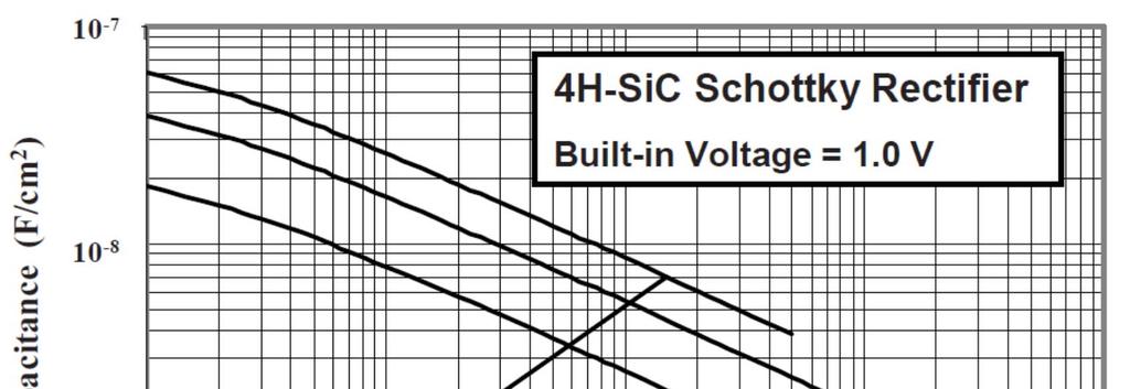
24 Device Capacitance (4H-SiC) 24
25 Summary The physics of operation of the Schottky rectifier has been described in this chapter. For power devices with relatively high breakdown voltages, the dominant current conduction mechanism is by the thermionic emission process. This process governs the fundamental relationship between the on-state voltage drop and the leakage current for power Schottky rectifiers. For power Schottky rectifiers, it is necessary to include the impact of the series resistance of the drift region on the on-state voltage drop. This series resistance limits the performance of silicon rectifiers to a breakdown voltage of less than 200 V. Sections is not discussed in detail; Sections 4.4.4, 4.6 to 4.10, and the Simulation Eample in Section 4.3 are not discussed in Chapter 4, hence they are not covered by the eam! Problems 4.9 and 4.12 at the end of Chapter 4 are not required! 25
Introduction to Power Semiconductor Devices
 ECE442 Power Semiconductor Devices and Integrated Circuits Introduction to Power Semiconductor Devices Zheng Yang (ERF 3017, email: yangzhen@uic.edu) Power Semiconductor Devices Applications System Ratings
PHYSICAL ELECTRONICS(ECE3540) CHAPTER 9 METAL SEMICONDUCTOR AND SEMICONDUCTOR HETERO-JUNCTIONS
 CHAPTER 9 METAL SEMICONDUCTOR AND SEMICONDUCTOR HETERO-JUNCTIONS") PHYSICAL ELECTRONICS(ECE3540) CHAPTER 9 METAL SEMICONDUCTOR AND SEMICONDUCTOR HETERO-JUNCTIONS Tennessee Technological University Wednesday, October 30, 013 1 Introduction Chapter 4: we considered the
PHYSICAL ELECTRONICS(ECE3540) CHAPTER 9 METAL SEMICONDUCTOR AND SEMICONDUCTOR HETERO-JUNCTIONS Tennessee Technological University Wednesday, October 30, 013 1 Introduction Chapter 4: we considered the
PHYSICAL ELECTRONICS(ECE3540) CHAPTER 9 METAL SEMICONDUCTOR AND SEMICONDUCTOR HETERO-JUNCTIONS
 CHAPTER 9 METAL SEMICONDUCTOR AND SEMICONDUCTOR HETERO-JUNCTIONS") PHYSICAL ELECTRONICS(ECE3540) CHAPTER 9 METAL SEMICONDUCTOR AND SEMICONDUCTOR HETERO-JUNCTIONS Tennessee Technological University Monday, November 11, 013 1 Introduction Chapter 4: we considered the semiconductor
PHYSICAL ELECTRONICS(ECE3540) CHAPTER 9 METAL SEMICONDUCTOR AND SEMICONDUCTOR HETERO-JUNCTIONS Tennessee Technological University Monday, November 11, 013 1 Introduction Chapter 4: we considered the semiconductor
Avalanche breakdown. Impact ionization causes an avalanche of current. Occurs at low doping
 Avalanche breakdown Impact ionization causes an avalanche of current Occurs at low doping Zener tunneling Electrons tunnel from valence band to conduction band Occurs at high doping Tunneling wave decays
8. Schottky contacts / JFETs
 Technische Universität Graz Institute of Solid State Physics 8. Schottky contacts / JFETs Nov. 21, 2018 Technische Universität Graz Institute of Solid State Physics metal - semiconductor contacts Photoelectric
Schottky diodes. JFETs - MESFETs - MODFETs
 Technische Universität Graz Institute of Solid State Physics Schottky diodes JFETs - MESFETs - MODFETs Quasi Fermi level When the charge carriers are not in equilibrium the Fermi energy can be different
Current mechanisms Exam January 27, 2012
 Current mechanisms Exam January 27, 2012 There are four mechanisms that typically cause currents to flow: thermionic emission, diffusion, drift, and tunneling. Explain briefly which kind of current mechanisms
Session 6: Solid State Physics. Diode
 Session 6: Solid State Physics Diode 1 Outline A B C D E F G H I J 2 Definitions / Assumptions Homojunction: the junction is between two regions of the same material Heterojunction: the junction is between
Metal Semiconductor Contacts
 Metal Semiconductor Contacts The investigation of rectification in metal-semiconductor contacts was first described by Braun [33-35], who discovered in 1874 the asymmetric nature of electrical conduction
Semiconductor Physics and Devices
 The pn Junction 1) Charge carriers crossing the junction. 3) Barrier potential Semiconductor Physics and Devices Chapter 8. The pn Junction Diode 2) Formation of positive and negative ions. 4) Formation
Lecture 04 Review of MOSFET
 ECE 541/ME 541 Microelectronic Fabrication Techniques Lecture 04 Review of MOSFET Zheng Yang (ERF 3017, email: yangzhen@uic.edu) What is a Transistor? A Switch! An MOS Transistor V GS V T V GS S Ron D
Chapter 7. The pn Junction
 Chapter 7 The pn Junction Chapter 7 PN Junction PN junction can be fabricated by implanting or diffusing donors into a P-type substrate such that a layer of semiconductor is converted into N type. Converting
For the following statements, mark ( ) for true statement and (X) for wrong statement and correct it.
 for true statement and (X) for wrong statement and correct it.") Benha University Faculty of Engineering Shoubra Electrical Engineering Department First Year communications. Answer all the following questions Illustrate your answers with sketches when necessary. The
Benha University Faculty of Engineering Shoubra Electrical Engineering Department First Year communications. Answer all the following questions Illustrate your answers with sketches when necessary. The
Semiconductor Device Physics
 1 emiconductor Device Physics Lecture 8 http://zitompul.wordpress.com 2 0 1 3 emiconductor Device Physics 2 M Contacts and chottky Diodes 3 M Contact The metal-semiconductor (M) contact plays a very important
Consider a uniformly doped PN junction, in which one region of the semiconductor is uniformly doped with acceptor atoms and the adjacent region is
 CHAPTER 7 The PN Junction Consider a uniformly doped PN junction, in which one region of the semiconductor is uniformly doped with acceptor atoms and the adjacent region is uniformly doped with donor atoms.
Effective masses in semiconductors
 Effective masses in semiconductors The effective mass is defined as: In a solid, the electron (hole) effective mass represents how electrons move in an applied field. The effective mass reflects the inverse
EECS130 Integrated Circuit Devices
 EECS130 Integrated Circuit Devices Professor Ali Javey 10/02/2007 MS Junctions, Lecture 2 MOS Cap, Lecture 1 Reading: finish chapter14, start chapter16 Announcements Professor Javey will hold his OH at
Review Energy Bands Carrier Density & Mobility Carrier Transport Generation and Recombination
 Review Energy Bands Carrier Density & Mobility Carrier Transport Generation and Recombination The Metal-Semiconductor Junction: Review Energy band diagram of the metal and the semiconductor before (a)
Module-6: Schottky barrier capacitance-impurity concentration
 6.1 Introduction: Module-6: Schottky barrier capacitance-impurity concentration The electric current flowing across a metal semiconductor interface is generally non-linear with respect to the applied bias
Semiconductor Physics. Lecture 6
 Semiconductor Physics Lecture 6 Recap pn junction and the depletion region Driven by the need to have no gradient in the fermi level free carriers migrate across the pn junction leaving a region with few
Semiconductor Junctions
 8 Semiconductor Junctions Almost all solar cells contain junctions between different materials of different doping. Since these junctions are crucial to the operation of the solar cell, we will discuss
ECE 340 Lecture 35 : Metal- Semiconductor Junctions Class Outline:
 ECE 340 Lecture 35 : - Junctions Class Outline: Ideal - Contacts Rectifying Contacts Ohmic Contacts Things you should know when you leave Key Questions What happens to the bands when we make contact between
EE 130 Intro to MS Junctions Week 6 Notes. What is the work function? Energy to excite electron from Fermi level to the vacuum level
 EE 13 Intro to S Junctions eek 6 Notes Problem 1 hat is the work function? Energy to ecite electron from Fermi level to the vacuum level Electron affinity of 4.5eV Electron affinity of Ge 4.eV orkfunction
Sample Exam # 2 ECEN 3320 Fall 2013 Semiconductor Devices October 28, 2013 Due November 4, 2013
 Sample Exam # 2 ECEN 3320 Fall 203 Semiconductor Devices October 28, 203 Due November 4, 203. Below is the capacitance-voltage curve measured from a Schottky contact made on GaAs at T 300 K. Figure : Capacitance
Lecture 17 - p-n Junction. October 11, Ideal p-n junction in equilibrium 2. Ideal p-n junction out of equilibrium
 6.72J/3.43J - Integrated Microelectronic Devices - Fall 22 Lecture 17-1 Lecture 17 - p-n Junction October 11, 22 Contents: 1. Ideal p-n junction in equilibrium 2. Ideal p-n junction out of equilibrium
Solid State Electronics. Final Examination
 The University of Toledo EECS:4400/5400/7400 Solid State Electronic Section elssf08fs.fm - 1 Solid State Electronics Final Examination Problems Points 1. 1. 14 3. 14 Total 40 Was the exam fair? yes no
Semiconductor Physics fall 2012 problems
 Semiconductor Physics fall 2012 problems 1. An n-type sample of silicon has a uniform density N D = 10 16 atoms cm -3 of arsenic, and a p-type silicon sample has N A = 10 15 atoms cm -3 of boron. For each
Semiconductor Physics fall 2012 problems
 Semiconductor Physics fall 2012 problems 1. An n-type sample of silicon has a uniform density N D = 10 16 atoms cm -3 of arsenic, and a p-type silicon sample has N A = 10 15 atoms cm -3 of boron. For each
Fundamentals of Semiconductor Physics
 Fall 2007 Fundamentals of Semiconductor Physics 万 歆 Zhejiang Institute of Modern Physics xinwan@zimp.zju.edu.cn http://zimp.zju.edu.cn/~xinwan/ Transistor technology evokes new physics The objective of
Final Examination EE 130 December 16, 1997 Time allotted: 180 minutes
 Final Examination EE 130 December 16, 1997 Time allotted: 180 minutes Problem 1: Semiconductor Fundamentals [30 points] A uniformly doped silicon sample of length 100µm and cross-sectional area 100µm 2
1 Name: Student number: DEPARTMENT OF PHYSICS AND PHYSICAL OCEANOGRAPHY MEMORIAL UNIVERSITY OF NEWFOUNDLAND. Fall :00-11:00
 1 Name: DEPARTMENT OF PHYSICS AND PHYSICAL OCEANOGRAPHY MEMORIAL UNIVERSITY OF NEWFOUNDLAND Final Exam Physics 3000 December 11, 2012 Fall 2012 9:00-11:00 INSTRUCTIONS: 1. Answer all seven (7) questions.
Figure 3.1 (p. 141) Figure 3.2 (p. 142)
 Figure 3.2 (p. 142)") Figure 3.1 (p. 141) Allowed electronic-energy-state systems for two isolated materials. States marked with an X are filled; those unmarked are empty. System 1 is a qualitative representation of a metal;
Figure 3.1 (p. 141) Allowed electronic-energy-state systems for two isolated materials. States marked with an X are filled; those unmarked are empty. System 1 is a qualitative representation of a metal;
ECE 340 Lecture 27 : Junction Capacitance Class Outline:
 ECE 340 Lecture 27 : Junction Capacitance Class Outline: Breakdown Review Junction Capacitance Things you should know when you leave M.J. Gilbert ECE 340 Lecture 27 10/24/11 Key Questions What types of
Lecture 13 - Carrier Flow (cont.), Metal-Semiconductor Junction. October 2, 2002
, Metal-Semiconductor Junction. October 2, 2002") 6.72J/3.43J - Integrated Microelectronic Devices - Fall 22 Lecture 13-1 Contents: Lecture 13 - Carrier Flow (cont.), Metal-Semiconductor Junction October 2, 22 1. Transport in space-charge and high-resistivity
6.72J/3.43J - Integrated Microelectronic Devices - Fall 22 Lecture 13-1 Contents: Lecture 13 - Carrier Flow (cont.), Metal-Semiconductor Junction October 2, 22 1. Transport in space-charge and high-resistivity
Spring Semester 2012 Final Exam
 Spring Semester 2012 Final Exam Note: Show your work, underline results, and always show units. Official exam time: 2.0 hours; an extension of at least 1.0 hour will be granted to anyone. Materials parameters
Semiconductor Devices
 Semiconductor Devices - 2014 Lecture Course Part of SS Module PY4P03 Dr. P. Stamenov School of Physics and CRANN, Trinity College, Dublin 2, Ireland Hilary Term, TCD 17 th of Jan 14 Metal-Semiconductor
Semiconductor Physics Problems 2015
 Semiconductor Physics Problems 2015 Page and figure numbers refer to Semiconductor Devices Physics and Technology, 3rd edition, by SM Sze and M-K Lee 1. The purest semiconductor crystals it is possible
SRI VIDYA COLLEGE OF ENGINEERING AND TECHNOLOGY VIRUDHUNAGAR Department of Electronics and Communication Engineering
 SRI VIDYA COLLEGE OF ENGINEERING AND TECHNOLOGY VIRUDHUNAGAR Department of Electronics and Communication Engineering Class/Sem:I ECE/II Question Bank for EC6201-ELECTRONIC DEVICES 1.What do u meant by
Electronic Devices and Circuits Lecture 5 - p-n Junction Injection and Flow - Outline
 6.012 - Electronic Devices and Circuits Lecture 5 - p-n Junction Injection and Flow - Outline Review Depletion approimation for an abrupt p-n junction Depletion charge storage and depletion capacitance
Sheng S. Li. Semiconductor Physical Electronics. Second Edition. With 230 Figures. 4) Springer
 Springer") Sheng S. Li Semiconductor Physical Electronics Second Edition With 230 Figures 4) Springer Contents Preface 1. Classification of Solids and Crystal Structure 1 1.1 Introduction 1 1.2 The Bravais Lattice
Sheng S. Li Semiconductor Physical Electronics Second Edition With 230 Figures 4) Springer Contents Preface 1. Classification of Solids and Crystal Structure 1 1.1 Introduction 1 1.2 The Bravais Lattice
Peak Electric Field. Junction breakdown occurs when the peak electric field in the PN junction reaches a critical value. For the N + P junction,
 Peak Electric Field Junction breakdown occurs when the peak electric field in the P junction reaches a critical value. For the + P junction, qa E ( x) ( xp x), s W dep 2 s ( bi Vr ) 2 s potential barrier
EECS130 Integrated Circuit Devices
 EECS130 Integrated Circuit Devices Professor Ali Javey 9/18/2007 P Junctions Lecture 1 Reading: Chapter 5 Announcements For THIS WEEK OLY, Prof. Javey's office hours will be held on Tuesday, Sept 18 3:30-4:30
ECE-342 Test 2 Solutions, Nov 4, :00-8:00pm, Closed Book (one page of notes allowed)
") ECE-342 Test 2 Solutions, Nov 4, 2008 6:00-8:00pm, Closed Book (one page of notes allowed) Please use the following physical constants in your calculations: Boltzmann s Constant: Electron Charge: Free
ECE-342 Test 2 Solutions, Nov 4, 2008 6:00-8:00pm, Closed Book (one page of notes allowed) Please use the following physical constants in your calculations: Boltzmann s Constant: Electron Charge: Free
junctions produce nonlinear current voltage characteristics which can be exploited
 Chapter 6 P-N DODES Junctions between n-and p-type semiconductors are extremely important foravariety of devices. Diodes based on p-n junctions produce nonlinear current voltage characteristics which can
Lecture 2. Introduction to semiconductors Structures and characteristics in semiconductors
 Lecture 2 Introduction to semiconductors Structures and characteristics in semiconductors Semiconductor p-n junction Metal Oxide Silicon structure Semiconductor contact Literature Glen F. Knoll, Radiation
CHAPTER 4: P-N P N JUNCTION Part 2. M.N.A. Halif & S.N. Sabki
 CHAPTER 4: P-N P N JUNCTION Part 2 Part 2 Charge Storage & Transient Behavior Junction Breakdown Heterojunction CHARGE STORAGE & TRANSIENT BEHAVIOR Once injected across the junction, the minority carriers
n N D n p = n i p N A
 Summary of electron and hole concentration in semiconductors Intrinsic semiconductor: E G n kt i = pi = N e 2 0 Donor-doped semiconductor: n N D where N D is the concentration of donor impurity Acceptor-doped
Schottky Diodes (M-S Contacts)
") Schottky Diodes (M-S Contacts) Three MITs of the Day Band diagrams for ohmic and rectifying Schottky contacts Similarity to and difference from bipolar junctions on electrostatic and IV characteristics.
Schottky Diodes (M-S Contacts) Three MITs of the Day Band diagrams for ohmic and rectifying Schottky contacts Similarity to and difference from bipolar junctions on electrostatic and IV characteristics.
This is the 15th lecture of this course in which we begin a new topic, Excess Carriers. This topic will be covered in two lectures.
 Solid State Devices Dr. S. Karmalkar Department of Electronics and Communication Engineering Indian Institute of Technology, Madras Lecture - 15 Excess Carriers This is the 15th lecture of this course
System Modeling and Characterization of SiC Schottky Power Diodes
 System Modeling and Characterization of SiC Schottky Power Diodes Hui Zhang, Student Member, IEEE, Leon M. Tolbert, Senior Member, IEEE, Burak Ozpineci, Senior Member, IEEE Abstract-Most of the present
Lecture 2. Introduction to semiconductors Structures and characteristics in semiconductors. Fabrication of semiconductor sensor
 Lecture 2 Introduction to semiconductors Structures and characteristics in semiconductors Semiconductor p-n junction Metal Oxide Silicon structure Semiconductor contact Fabrication of semiconductor sensor
UNIVERSITY OF CALIFORNIA College of Engineering Department of Electrical Engineering and Computer Sciences. EECS 130 Professor Ali Javey Fall 2006
 UNIVERSITY OF CALIFORNIA College of Engineering Department of Electrical Engineering and Computer Sciences EECS 130 Professor Ali Javey Fall 2006 Midterm 2 Name: SID: Closed book. Two sheets of notes are
The pn junction. [Fonstad, Ghione]
![The pn junction. [Fonstad, Ghione]](/thumbs/93/112370833.jpg "The pn junction. [Fonstad, Ghione]") The pn junction [Fonstad, Ghione] Band diagram On the vertical axis: potential energy of the electrons On the horizontal axis: now there is nothing: later we ll put the position qf s : work function (F
The pn junction [Fonstad, Ghione] Band diagram On the vertical axis: potential energy of the electrons On the horizontal axis: now there is nothing: later we ll put the position qf s : work function (F
Diodes. EE223 Digital & Analogue Electronics Derek Molloy 2012/2013.
 Diodes EE223 Digital & Analogue Electronics Derek Molloy 2012/2013 Derek.Molloy@dcu.ie Diodes: A Semiconductor? Conductors Such as copper, aluminium have a cloud of free electrons weak bound valence electrons
PN Junction
 P Junction 2017-05-04 Definition Power Electronics = semiconductor switches are used Analogue amplifier = high power loss 250 200 u x 150 100 u Udc i 50 0 0 50 100 150 200 250 300 350 400 i,u dc i,u u
High-temperature characteristics of SiC Schottky barrier diodes related to physical phenomena
 High-temperature characteristics of SiC Schottky barrier diodes related to physical phenomena Tsuyoshi Funaki 1a), Tsunenobu Kimoto 2, and Takashi Hikihara 1 1 Kyoto University, Dept. of Electrical Eng.
Introductory Nanotechnology ~ Basic Condensed Matter Physics ~
 Introductory Nanotechnology ~ Basic Condensed Matter Physics ~ Atsufumi Hirohata Department of Electronics Quick Review over the Last Lecture Classic model : Dulong-Petit empirical law c V, mol 3R 0 E
Bipolar junction transistor operation and modeling
 6.01 - Electronic Devices and Circuits Lecture 8 - Bipolar Junction Transistor Basics - Outline Announcements Handout - Lecture Outline and Summary; Old eam 1's on Stellar First Hour Eam - Oct. 8, 7:30-9:30
Diodes. anode. cathode. cut-off. Can be approximated by a piecewise-linear-like characteristic. Lecture 9-1
 Diodes mplest nonlinear circuit element Basic operation sets the foundation for Bipolar Junction Transistors (BJTs) Also present in Field Effect Transistors (FETs) Ideal diode characteristic anode cathode
Midterm I - Solutions
 UNIVERSITY OF CALIFORNIA College of Engineering Department of Electrical Engineering and Computer Sciences EECS 130 Spring 2008 Professor Chenming Hu Midterm I - Solutions Name: SID: Grad/Undergrad: Closed
Junction Diodes. Tim Sumner, Imperial College, Rm: 1009, x /18/2006
 Junction Diodes Most elementary solid state junction electronic devices. They conduct in one direction (almost correct). Useful when one converts from AC to DC (rectifier). But today diodes have a wide
Lecture 15 - The pn Junction Diode (I) I-V Characteristics. November 1, 2005
 I-V Characteristics. November 1, 2005") 6.012 - Microelectronic Devices and Circuits - Fall 2005 Lecture 15-1 Lecture 15 - The pn Junction Diode (I) I-V Characteristics November 1, 2005 Contents: 1. pn junction under bias 2. I-V characteristics
6.012 - Microelectronic Devices and Circuits - Fall 2005 Lecture 15-1 Lecture 15 - The pn Junction Diode (I) I-V Characteristics November 1, 2005 Contents: 1. pn junction under bias 2. I-V characteristics
Diodes for Power Electronic Applications
 Lecture Notes Diodes for Power Electronic Applications William P. Robbins Professor, Dept. of Electrical and Computer Engineering University of Minnesota OUTLINE PN junction power diode construction Breakdown
Electrical Characteristics of MOS Devices
 Electrical Characteristics of MOS Devices The MOS Capacitor Voltage components Accumulation, Depletion, Inversion Modes Effect of channel bias and substrate bias Effect of gate oide charges Threshold-voltage
PN Junctions. Lecture 7
 Lecture 7 PN Junctions Kathy Aidala Applied Physics, G2 Harvard University 10 October, 2002 Wei 1 Active Circuit Elements Why are they desirable? Much greater flexibility in circuit applications. What
Lecture 2. Introduction to semiconductors Structures and characteristics in semiconductors
 Lecture 2 Introduction to semiconductors Structures and characteristics in semiconductors Semiconductor p-n junction Metal Oxide Silicon structure Semiconductor contact Literature Glen F. Knoll, Radiation
ECEN 3320 Semiconductor Devices Final exam - Sunday December 17, 2000
 Your Name: ECEN 3320 Semiconductor Devices Final exam - Sunday December 17, 2000 1. Review questions a) Illustrate the generation of a photocurrent in a p-n diode by drawing an energy band diagram. Indicate
BJT - Mode of Operations
 JT - Mode of Operations JTs can be modeled by two back-to-back diodes. N+ P N- N+ JTs are operated in four modes. HO #6: LN 251 - JT M Models Page 1 1) Forward active / normal junction forward biased junction
p-n junction biasing, p-n I-V characteristics, p-n currents Norlaili Mohd. Noh EEE /09
 CLASS 6&7 p-n junction biasing, p-n I-V characteristics, p-n currents 1 p-n junction biasing Unbiased p-n junction: the potential barrier is 0.7 V for Si and 0.3 V for Ge. Nett current across the p-n junction
A New High Voltage 4H-SiC Lateral Dual Sidewall Schottky (LDSS) Rectifier: Theoretical Investigation and Analysis
 Rectifier: Theoretical Investigation and Analysis") M. Jagadesh Kumar and C. Linga Reddy, "A New High Voltage 4H-SiC Lateral Dual Sidewall Schottky (LDSS) Rectifier: Theoretical Investigation and Analysis", IEEE Trans. on Electron Devices, Vol.50, pp.1690-1693,
M. Jagadesh Kumar and C. Linga Reddy, "A New High Voltage 4H-SiC Lateral Dual Sidewall Schottky (LDSS) Rectifier: Theoretical Investigation and Analysis", IEEE Trans. on Electron Devices, Vol.50, pp.1690-1693,
PN Junction Diode. Diode Cases. Semiconductor Elements. 2009, EE141Associate Professor PhD. T.Vasileva
 PN Junction Diode Semiconductor Elements 1 Diode Cases 2 1 Basic Diode Feature The essential feature of a diode is at e magnitude of e current greatly depends on e polarity of applied voltage. Basicaly
Institute of Solid State Physics. Technische Universität Graz. Exam. Feb 2, 10:00-11:00 P2
 Technische Universität Graz nstitute of Solid State Physics Exam Feb 2, 10:00-11:00 P2 Exam Four questions, two from the online list. Calculator is ok. No notes. Explain some concept: (tunnel contact,
Section 12: Intro to Devices
 Section 12: Intro to Devices Extensive reading materials on reserve, including Robert F. Pierret, Semiconductor Device Fundamentals EE143 Ali Javey Bond Model of Electrons and Holes Si Si Si Si Si Si Si
Semiconductor Physical Electronics
 Semiconductor Physical Electronics Sheng S. Li Department of Electrical Engineering University of Florida Gainesville, Florida Plenum Press New York and London Contents CHAPTER 1. Classification of Solids
Thermionic emission vs. drift-diffusion vs. p-n junction
 6.772/SMA5111 - Compound Semiconductors Lecture 4 - Carrier flow in heterojunctions - Outline A look at current models for m-s junctions (old business) Thermionic emission vs. drift-diffusion vs. p-n junction
( )! N D ( x) ) and equilibrium
! N D ( x) ) and equilibrium") ECE 66: SOLUTIONS: ECE 66 Homework Week 8 Mark Lundstrom March 7, 13 1) The doping profile for an n- type silicon wafer ( N D = 1 15 cm - 3 ) with a heavily doped thin layer at the surface (surface concentration,
ECE 66: SOLUTIONS: ECE 66 Homework Week 8 Mark Lundstrom March 7, 13 1) The doping profile for an n- type silicon wafer ( N D = 1 15 cm - 3 ) with a heavily doped thin layer at the surface (surface concentration,
3. Two-dimensional systems
 3. Two-dimensional systems Image from IBM-Almaden 1 Introduction Type I: natural layered structures, e.g., graphite (with C nanostructures) Type II: artificial structures, heterojunctions Great technological
Lecture-4 Junction Diode Characteristics
 1 Lecture-4 Junction Diode Characteristics Part-II Q: Aluminum is alloyed into n-type Si sample (N D = 10 16 cm 3 ) forming an abrupt junction of circular cross-section, with an diameter of 0.02 in. Assume
Long Channel MOS Transistors
 Long Channel MOS Transistors The theory developed for MOS capacitor (HO #2) can be directly extended to Metal-Oxide-Semiconductor Field-Effect transistors (MOSFET) by considering the following structure:
PN Junction and MOS structure
 PN Junction and MOS structure Basic electrostatic equations We will use simple one-dimensional electrostatic equations to develop insight and basic understanding of how semiconductor devices operate Gauss's
OPTI510R: Photonics. Khanh Kieu College of Optical Sciences, University of Arizona Meinel building R.626
 OPTI510R: Photonics Khanh Kieu College of Optical Sciences, University of Arizona kkieu@optics.arizona.edu Meinel building R.626 Announcements Homework #6 is assigned, due May 1 st Final exam May 8, 10:30-12:30pm
L03: pn Junctions, Diodes
 8/30/2012 Page 1 of 5 Reference:C:\Users\Bernhard Boser\Documents\Files\Lib\MathCAD\Default\defaults.mcd L03: pn Junctions, Diodes Intrinsic Si Q: What are n, p? Q: Is the Si charged? Q: How could we make
Semiconductor Detectors
 Semiconductor Detectors Summary of Last Lecture Band structure in Solids: Conduction band Conduction band thermal conductivity: E g > 5 ev Valence band Insulator Charge carrier in conductor: e - Charge
1st Year-Computer Communication Engineering-RUC. 4- P-N Junction
 4- P-N Junction We begin our study of semiconductor devices with the junction for three reasons. (1) The device finds application in many electronic systems, e.g., in adapters that charge the batteries
Thermionic Emission Theory
 hapter 4. PN and Metal-Semiconductor Junction Thermionic Emiion Theory Energy band diagram of a Schottky contact with a forward bia V applied between the metal and the emiconductor. Electron concentration
Lecture 19 - p-n Junction (cont.) October 18, Ideal p-n junction out of equilibrium (cont.) 2. pn junction diode: parasitics, dynamics
 October 18, Ideal p-n junction out of equilibrium (cont.) 2. pn junction diode: parasitics, dynamics") 6.720J/3.43J - Integrated Microelectronic Devices - Fall 2002 Lecture 19-1 Lecture 19 - p-n Junction (cont.) October 18, 2002 Contents: 1. Ideal p-n junction out of equilibrium (cont.) 2. pn junction diode:
6.720J/3.43J - Integrated Microelectronic Devices - Fall 2002 Lecture 19-1 Lecture 19 - p-n Junction (cont.) October 18, 2002 Contents: 1. Ideal p-n junction out of equilibrium (cont.) 2. pn junction diode:
MTLE-6120: Advanced Electronic Properties of Materials. Semiconductor p-n junction diodes. Reading: Kasap ,
 MTLE-6120: Advanced Electronic Properties of Materials 1 Semiconductor p-n junction diodes Reading: Kasap 6.1-6.5, 6.9-6.12 Metal-semiconductor contact potential 2 p-type n-type p-type n-type Same semiconductor
Unit IV Semiconductors Engineering Physics
 Introduction A semiconductor is a material that has a resistivity lies between that of a conductor and an insulator. The conductivity of a semiconductor material can be varied under an external electrical
UNIVERSITY OF CALIFORNIA College of Engineering Department of Electrical Engineering and Computer Sciences. Professor Chenming Hu.
 UNIVERSITY OF CALIFORNIA College of Engineering Department of Electrical Engineering and Computer Sciences EECS 130 Spring 2009 Professor Chenming Hu Midterm I Name: Closed book. One sheet of notes is
6.012 Electronic Devices and Circuits
 Page 1 of 1 YOUR NAME Department of Electrical Engineering and Computer Science Massachusetts Institute of Technology 6.12 Electronic Devices and Circuits Exam No. 1 Wednesday, October 7, 29 7:3 to 9:3
Appendix 1: List of symbols
 Appendix 1: List of symbols Symbol Description MKS Units a Acceleration m/s 2 a 0 Bohr radius m A Area m 2 A* Richardson constant m/s A C Collector area m 2 A E Emitter area m 2 b Bimolecular recombination
Review of Semiconductor Fundamentals
 ECE 541/ME 541 Microelectronic Fabrication Techniques Review of Semiconductor Fundamentals Zheng Yang (ERF 3017, email: yangzhen@uic.edu) Page 1 Semiconductor A semiconductor is an almost insulating material,
ECE PN Junctions and Diodes
 ECE 342 2. PN Junctions and iodes Jose E. Schutt-Aine Electrical & Computer Engineering University of Illinois jschutt@emlab.uiuc.edu ECE 342 Jose Schutt Aine 1 B: material dependent parameter = 5.4 10
Electronic Supplementary Information. Recombination kinetics in silicon solar cell under low-concentration: Electroanalytical
 Electronic Supplementary Material (ESI) for Physical Chemistry Chemical Physics. This journal is the Owner Societies 2014 Electronic Supplementary Information Recombination kinetics in silicon solar cell
UNIVERSITY OF CALIFORNIA College of Engineering Department of Electrical Engineering and Computer Sciences. EECS 130 Professor Ali Javey Fall 2006
 UNIVERSITY OF CALIFORNIA College of Engineering Department of Electrical Engineering and Computer Sciences EECS 130 Professor Ali Javey Fall 2006 Midterm I Name: Closed book. One sheet of notes is allowed.
Lecture 9: Metal-semiconductor junctions
 Lecture 9: Metal-semiconductor junctions Contents 1 Introduction 1 2 Metal-metal junction 1 2.1 Thermocouples.......................... 2 3 Schottky junctions 4 3.1 Forward bias............................
EE 5611 Introduction to Microelectronic Technologies Fall Tuesday, September 23, 2014 Lecture 07
 EE 5611 Introduction to Microelectronic Technologies Fall 2014 Tuesday, September 23, 2014 Lecture 07 1 Introduction to Solar Cells Topics to be covered: Solar cells and sun light Review on semiconductor
Electrons are shared in covalent bonds between atoms of Si. A bound electron has the lowest energy state.
 Photovoltaics Basic Steps the generation of light-generated carriers; the collection of the light-generated carriers to generate a current; the generation of a large voltage across the solar cell; and
ECE 442. Spring, Lecture -2
 ECE 442 Power Semiconductor Devices and Integrated circuits Spring, 2006 University of Illinois at Chicago Lecture -2 Semiconductor physics band structures and charge carriers 1. What are the types of
Basic Physics of Semiconductors
 Basic Physics of Semiconductors Semiconductor materials and their properties PN-junction diodes Reverse Breakdown EEM 205 Electronics I Dicle University, EEE Dr. Mehmet Siraç ÖZERDEM Semiconductor Physics