Review of Semiconductor Drift Detectors
|
|
|
- Barnard Wright
- 6 years ago
- Views:
Transcription
1 Pavia October 25, 2004 Review of Semiconductor Drift Detectors Talk given by Pavel Rehak following a presentation on 5 th Hiroshima Symposium of Semiconductor Tracking Detectors
2 Outline of the Review Principles of Semiconductor Drift Detectors Drift Detectors for Position and Charge sensing Lessons learned from utilization of Drift Detectors in Heavy Ion Experiments X-ray spectroscopy with Drift Detectors Controlled Drift Detectors Conclusions and predictions
3 Concept of Semiconductor Drift Detector Transport of charged carriers in thin fully depleted semiconductor detectors in direction parallel to the large surface of the detector. 0.3 mm Ionizing particle Drift of charged carriers in silicon Drift < 40mm Anode 1.) Charge carriers induce a signal on the anode only on the arrival. The drift time measure the distance between the position of the ionizing particle and the anode. 2.) The capacitance of the anode is small -> low series noise of the read-out.
4 Analyses of buried channel Charge Coupled Devices. (CCDs) in 1983 Negative potential in the region of the channel.
5 Reversed biased one sided step p-n junction in 1dimension Space charge region Neutral region Space charge density ρ ρ=qn N is donor or acceptor volume density
6 Equations of electrostatics Negative electric field -E div E=ρ/ε In one dimensional case the above reduces into: de/dx=ρ/ε Electric field is a piecewise linear. Electric potential U is defined by: Negative potential -U E=-grad U In one dimensional case the above reduces into: E=-dU/dx U is parabolic and depleted depth d d = 2εU / qn

7 Depletion from two sides P+ rectifying contacts N+ ohmic contacts n- bulk Section shown below Undepleted region(s)
8 Summary of principles Anodes Rectifying electrodes Ionizing particle Unambiguous 2 dimensional measur. Precision: 2um in lab 10 um in the test beam 20 um in experiments
9 Optimal signal processing 2 ε = , C e n / 2 w ( t) dt + q ν w ( t) dt + q N q N f '( t) w( t) dt f ( t) w 2 ( t) dt Where: w(t) is unknown weighting function, f(t) is pulse shape induced on the anode normalized to the area of 1, N is the number of electrons in the signal pulse, C total input capacitance, e_n^2 physical spectral density of the series noise, νq is the leakage current and q is the positive value of charge of an electron. To minimize the above time variance can be reduced to the solution of the following equation: C 2 2 e 2 f ( t) 2ν n w t + w t + w ( t ) = 2 2 "( ) ( ) ε f '( t ) min const q N N N
10 Position sensing in high energy heavy ion experiments NA45 (CERES) Experiment at SPS at CERN a) 3 cylindrical drift detector and b) 4 cylindrical detector (past) STAR Experiment at RHIC at BNL (present) ALICE Experiment at LHC at CERN (future)
11
12
13 Innovations in CERES cyl. Det. Collection of leakage current generated at the Si-SiO interface at a sink anode Interlaced anodes (Nyquist filtering in linear dimension) 366 um 1 degree 122 um 61 um

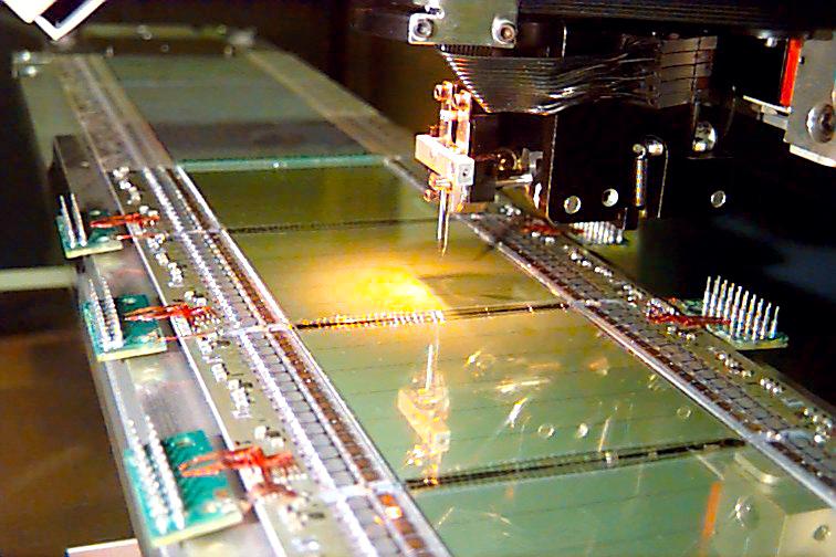
14 STAR Drift Detector
15
16 SDD collaboration INFN - Turin Italy INFN - Trieste - Italy INFN - Bologna Italy INFN - Rome Italy INFN - Alessandria- Italy Ohio State University - Columbus - Ohio - USA University of Jyvaskyla - Jyvaskyla - Finland Nat. Acad. of Sciences, Bogolyubov Inst. for Th. Phys. - Kiev - Ukraine Scientific Res. Techn. Inst. of Instrument Making - Kharkov - Ukraine Acad. of Sciences of Czech Republic - Rez U Prahy - Czech Republic St. Petersburg State University - St. Petersburg - Russia
 Ladders SDDs per ladder Layer 3 14.9 14 6 Layer 4 23.8 22 8")
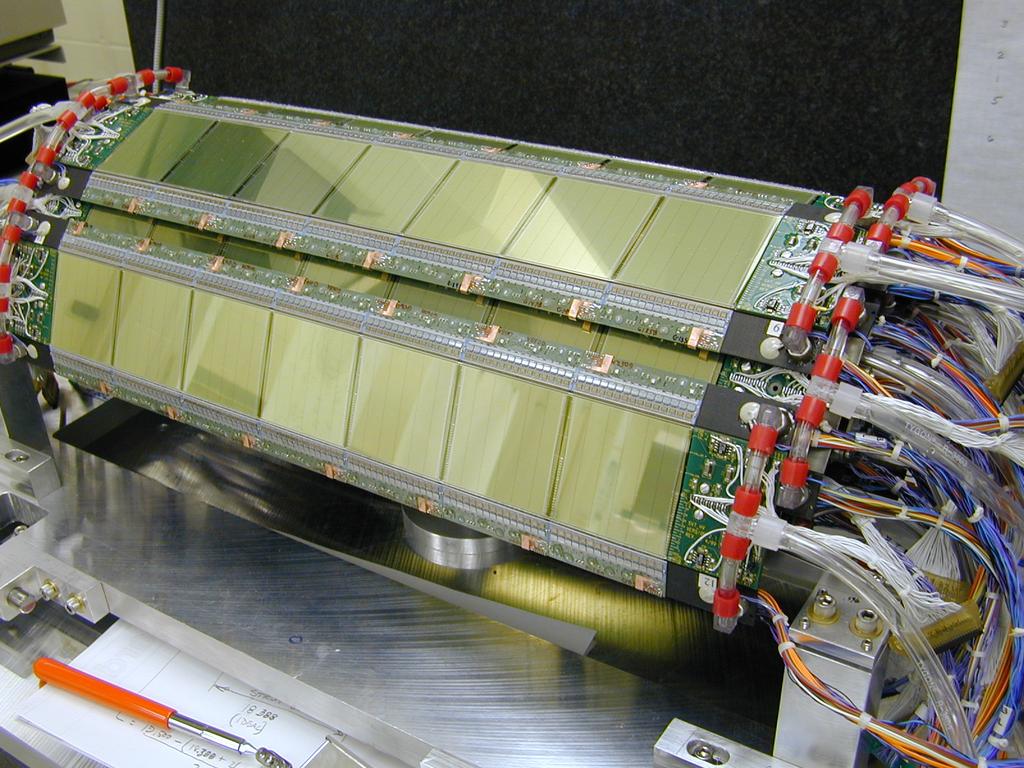
17 SDD barrels Silicon Drift Detectors Tot. No. channels Tot. No. detectors 260 total area 1.37 m 2 Radius (mm) Ladders SDDs per ladder Layer Layer
 silicon, 3 kω cm resistivity, 300 µm thickness Active area: 7.02 7.")
18 ALICE Silicon Drift Detector Drift Drift segmented 2 x 256 anodes Wafer: 5, Neutron Transmutation Doped (NTD) silicon, 3 kω cm resistivity, 300 µm thickness Active area: cm 2 (83% to total)

 implanted HV voltage dividers 256")

19 Detector design features injector lines Charge collection zone guard cathodes (32 µm m pitch) 292 drift cathodes (120 µm m pitch) implanted HV voltage dividers 256 collection anodes (294 µm m pitch) injector line bonding pad MOS injector (every 8 th anode)
20 Beam Tests in 2003 Position resolution Exhaustive test of the front-end parameters performed in beam test:gain, sampling & ADC frequencies...
21 Linear absorption coefficient Abs. coeff. (1/cm) Photon energy (kev)
22 σ 2 = F E w Si photon ENC 2 = qi par leak 2 = 1 e 2 C 2 series 2 n t ENC t ( optimal) peak h( t) 2 dt qi leak t peak [ ] h ' 2 ( t) dt e 2 C 2 / t n t peak = e C / n w = 3. 62eV t q I leak

23 Leakage Current: ileak = q ni /( 2 τ) Where n_i is the density of carrier in intrinsic silicon, tau is the life time and N_t the density of traps in silicon bulk. n i exp( E gap τ 1/( σ vth Nt ) /(2kT))

24 X-ray drift detector


25 Potential within Drift Detectors
26 Single sided junction FET
27 The best room temp. spectrum
28 Low energy tails

29 X-ray fluorescence system

30 Applications in Art studies
 INTEGRATION - low capacitance (~100fF) and integrated JFET high energy resolution LV LV + CK n-type epitaxial layer 50 Ω cm 15 µ m 280 µ m LV - CK p")
 - integrate-readout mode n-type substrate 3kΩ cm channel-stop (deep p-implants) Integration phase hν Readout phase ~ 3µs/cm The")
31 The Controlled-Drift Detector (CDD)* (*) Patents: US 6,249,033 EP (-V) CK drift integration V DRIFT V HV HV + CK p +strips HV - CK - 2D position sensing ( µm) INTEGRATION - low capacitance (~100fF) and integrated JFET high energy resolution LV LV + CK n-type epitaxial layer 50 Ω cm 15 µ m 280 µ m LV - CK p +entrance window - low no. of channels (n instead of n n ) - integrate-readout mode n-type substrate 3kΩ cm channel-stop (deep p-implants) Integration phase hν Readout phase ~ 3µs/cm The X-ray position along the drift is obtained from the electrons drift time The X-ray energy is obtained from the electron charge collected at the anodes
32 Transport mechanism and Readout speed Charge-Coupled Device (CCD) L.Strüder et al., NIM A257 (1987) 594 Controlled Drift Detector A.Castoldi et al., IEEE TNS, 44(5) oct p.1724 long readout time as charge transfer and processing are done sequentially shorter readout time as charge transfer and processing are simultaneous T readout = N pixel (T proc + t tr ) ~ 1 ms/cm T readout = T drift ~ 3 µs/cm
 June 2002 ns ns t t == 55 55 counts 4000 FWHM = 11 ns FWHM = 11 ns integration readout 9 µs 1µs 2000 Frame frequency=100 khz 0 9000 Pixel 180µm x 180µm 8000 ~250 ev FWHM @ 300K eletrons r.m.s.) 277.")
33 1-D imaging and spectroscopy of a Fe khz A.Castoldi, C.Guazzoni, P.Rehak, L.Strüder, Trans. Nucl. Sci. 49 (3) June 2002 ns ns t t == counts 4000 FWHM = 11 ns FWHM = 11 ns integration readout 9 µs 1µs 2000 Frame frequency=100 khz Pixel 180µm x 180µm 8000 ~250 ev 300K eletrons r.m.s.) ev FHWM (29.6 el. rms) (ENC=26 Energy [ev] Tsh=0.25 µs x6 mm2 prototype time [µs] E+0 5E+3 counts 1E+4


34 X-ray spectroscopic imaging with CDDs Radiographic image of a lizard*... pixel 120µm, 10 5 frame/s, T=300 K Sincrotrone Trieste * no animal was killed ot has suffered for this measurement and spectroscopic analysis of each pixel 250 ev 300K Energy [kev]
35 Readout speed and Energy resolution A fast readout speed allows to reduce both readout and integration times: higher frame rate (i.e. better time resolution between X-ray images) better energy resolution at room temperature due to lower integrated leakage charge. ENC [electrons] SLOW READOUT f frame = 500 Hz f frame = 10 KHz f frame = 100 KHz f frame = 2 KHz f frame =5 KHz FAST READOUT T [K] Time-resolved imaging at frame frequency greater than 10 khz State-of-the-art energy resolution near room T
36 Summary and Conclusions Extended use of SDD for tracking in high energy heavy ions experiments Industrial use of Silicon Drift Detectors for X-ray fluoroscopy Development of Controlled Drift Detector Use of Drift concept for Detectors on High Z materials. (insensitive to hole trapping) Future-high resistivity silicon for X-rays Future tracking with electronics grade Si
Controlled Si-Drift Detectors
 Controlled Si-Drift Detectors A.Castoldi Politecnico di Milano and INFN sez. Milano E-mail: andrea.castoldi@polimi.it Brookhaven National Laboratory, NY MPI Halbleiterlabor, Munich -potential [V] 65 60
Lecture 18. New gas detectors Solid state trackers
 Lecture 18 New gas detectors Solid state trackers Time projection Chamber Full 3-D track reconstruction x-y from wires and segmented cathode of MWPC z from drift time de/dx information (extra) Drift over
Semiconductor X-Ray Detectors. Tobias Eggert Ketek GmbH
 Semiconductor X-Ray Detectors Tobias Eggert Ketek GmbH Semiconductor X-Ray Detectors Part A Principles of Semiconductor Detectors 1. Basic Principles 2. Typical Applications 3. Planar Technology 4. Read-out
Solid State Detectors
 Solid State Detectors Most material is taken from lectures by Michael Moll/CERN and Daniela Bortoletto/Purdue and the book Semiconductor Radiation Detectors by Gerhard Lutz. In gaseous detectors, a charged
Semiconductor Detectors
 Semiconductor Detectors Summary of Last Lecture Band structure in Solids: Conduction band Conduction band thermal conductivity: E g > 5 ev Valence band Insulator Charge carrier in conductor: e - Charge
Components of a generic collider detector
 Lecture 24 Components of a generic collider detector electrons - ionization + bremsstrahlung photons - pair production in high Z material charged hadrons - ionization + shower of secondary interactions
Lecture 8. Detectors for Ionizing Particles
 Lecture 8 Detectors for Ionizing Particles Content Introduction Overview of detector systems Sources of radiation Radioactive decay Cosmic Radiation Accelerators Interaction of Radiation with Matter General
Lecture 2. Introduction to semiconductors Structures and characteristics in semiconductors
 Lecture 2 Introduction to semiconductors Structures and characteristics in semiconductors Semiconductor p-n junction Metal Oxide Silicon structure Semiconductor contact Literature Glen F. Knoll, Radiation
Silicon Drift Detectors: Understanding the Advantages for EDS Microanalysis. Patrick Camus, PhD Applications Scientist March 18, 2010
 Silicon Drift Detectors: Understanding the Advantages for EDS Microanalysis Patrick Camus, PhD Applications Scientist March 18, 2010 EDS Detector Requirements Detect whole energy range of x-rays 50 ev
Lecture 2. Introduction to semiconductors Structures and characteristics in semiconductors
 Lecture 2 Introduction to semiconductors Structures and characteristics in semiconductors Semiconductor p-n junction Metal Oxide Silicon structure Semiconductor contact Literature Glen F. Knoll, Radiation
GEM at CERN. Leszek Ropelewski CERN PH-DT2 DT2-ST & TOTEM
 GEM at CERN Leszek Ropelewski CERN PH-DT2 DT2-ST & TOTEM MicroStrip Gas Chamber Semiconductor industry technology: Photolithography Etching Coating Doping A. Oed Nucl. Instr. and Meth. A263 (1988) 351.
Development and characterization of 3D semiconductor X-rays detectors for medical imaging
 Development and characterization of 3D semiconductor X-rays detectors for medical imaging Marie-Laure Avenel, Eric Gros d Aillon CEA-LETI, DETectors Laboratory marie-laure.avenel@cea.fr Outlines Problematic
Czech Technical University in Prague Faculty of Nuclear Sciences and Physical Engineering
 Czech Technical University in Prague Faculty of Nuclear Sciences and Physical Engineering Department of Physics Silicon Drift Detectors Review Work Jiří Král Supervisor: RNDr. Vojtěch Petráček Table of
Development of High-Z Semiconductor Detectors and Their Applications to X-ray/gamma-ray Astronomy
 Development of High-Z Semiconductor Detectors and Their Applications to X-ray/gamma-ray Astronomy Taka Tanaka (SLAC/KIPAC) 9/19/2007 SLAC Advanced Instrumentation Seminar Outline Introduction CdTe Diode
Classification of Solids
 Classification of Solids Classification by conductivity, which is related to the band structure: (Filled bands are shown dark; D(E) = Density of states) Class Electron Density Density of States D(E) Examples
Charge Collection and Capacitance-Voltage analysis in irradiated n-type magnetic Czochralski silicon detectors
 Charge Collection and Capacitance-Voltage analysis in irradiated n-type magnetic Czochralski silicon detectors M. K. Petterson, H.F.-W. Sadrozinski, C. Betancourt SCIPP UC Santa Cruz, 1156 High Street,
Semiconductor-Detectors
 Semiconductor-Detectors 1 Motivation ~ 195: Discovery that pn-- junctions can be used to detect particles. Semiconductor detectors used for energy measurements ( Germanium) Since ~ 3 years: Semiconductor
Silicon Drift Detectors for gamma-ray detection: 15 years of research (and collaboration between Politecnico and INAF-Milano)
") Silicon Drift Detectors for gamma-ray detection: 15 years of research (and collaboration between Politecnico and INAF-Milano) Outline The Silicon Drift Detector (SDD) Gamma-ray detectors based on scintillators
Silicon Drift Detectors for gamma-ray detection: 15 years of research (and collaboration between Politecnico and INAF-Milano) Outline The Silicon Drift Detector (SDD) Gamma-ray detectors based on scintillators
Semiconductor Detectors are Ionization Chambers. Detection volume with electric field Energy deposited positive and negative charge pairs
 1 V. Semiconductor Detectors V.1. Principles Semiconductor Detectors are Ionization Chambers Detection volume with electric field Energy deposited positive and negative charge pairs Charges move in field
M. De Napoli, F. Giacoppo, G. Raciti, E. Rapisarda, C. Sfienti. Laboratori Nazionali del Sud (LNS) INFN University of Catania. IPRD Oct.
 INFN University of Catania. IPRD Oct.") M. De Napoli, F. Giacoppo, G. Raciti, E. Rapisarda, C. Sfienti Laboratori Nazionali del Sud (LNS) INFN University of Catania IPRD08 1-4 Oct. Siena Silicon carbide (SiC) is expected to be applied to high-power
M. De Napoli, F. Giacoppo, G. Raciti, E. Rapisarda, C. Sfienti Laboratori Nazionali del Sud (LNS) INFN University of Catania IPRD08 1-4 Oct. Siena Silicon carbide (SiC) is expected to be applied to high-power
Gamma-ray Spectroscopy with LaBr 3 :Ce Scintillator Readout by a Silicon Drift Detector
 Gamma-ray Spectroscopy with LaBr 3 :Ce Scintillator Readout by a Silicon Drift Detector C. Fiorini, member, IEEE, A. Gola, M. Zanchi, A. Longoni, P. Lechner, H. Soltau, L. Strüder Abstract In this work
Chap. 11 Semiconductor Diodes
 Chap. 11 Semiconductor Diodes Semiconductor diodes provide the best resolution for energy measurements, silicon based devices are generally used for charged-particles, germanium for photons. Scintillators
Simulation results from double-sided and standard 3D detectors
 Simulation results from double-sided and standard 3D detectors David Pennicard, University of Glasgow Celeste Fleta, Chris Parkes, Richard Bates University of Glasgow G. Pellegrini, M. Lozano - CNM, Barcelona
Energetic particles and their detection in situ (particle detectors) Part II. George Gloeckler
 Part II. George Gloeckler") Energetic particles and their detection in situ (particle detectors) Part II George Gloeckler University of Michigan, Ann Arbor, MI University of Maryland, College Park, MD Simple particle detectors Gas-filled
Energetic particles and their detection in situ (particle detectors) Part II George Gloeckler University of Michigan, Ann Arbor, MI University of Maryland, College Park, MD Simple particle detectors Gas-filled
Solid State Detectors Semiconductor detectors Halbleiterdetektoren
 Solid State Detectors Semiconductor detectors Halbleiterdetektoren Doris Eckstein DESY Where are solid state detectors used? > Nuclear Physics: Energy measurement of charged particles (particles up to
Mara Bruzzi INFN and University of Florence, Italy and SCIPP, UC Santa Cruz, USA
 SCIPP 06/16 September 2006 Capacitance-Voltage analysis at different temperatures in heavily irradiated silicon detectors Mara Bruzzi INFN and University of Florence, Italy and SCIPP, UC Santa Cruz, USA
Detectors for High Energy Physics
 Detectors for High Energy Physics Ingrid-Maria Gregor, DESY DESY Summer Student Program 2017 Hamburg July 26th/27th Overview I. Detectors for Particle Physics II. Interaction with Matter } Wednesday III.
arxiv: v2 [nucl-ex] 6 Oct 2008
![arxiv: v2 [nucl-ex] 6 Oct 2008](/thumbs/88/114593371.jpg "arxiv: v2 [nucl-ex] 6 Oct 2008") he ime Projection Chamber for the ALICE Experiment C. Lippmann and the ALICE PC Collaboration CERN, 1211 Geneva 23, Switzerland he ime Projection Chamber of the ALICE Experiment has been installed in the
he ime Projection Chamber for the ALICE Experiment C. Lippmann and the ALICE PC Collaboration CERN, 1211 Geneva 23, Switzerland he ime Projection Chamber of the ALICE Experiment has been installed in the
New trends in CdTe detectors for X and γ-ray applications
 New trends in CdTe detectors for X and γ-ray applications Olivier Limousin CEA Saclay / DSM / DAPNIA Service d Astrophysique France New developments in photodetection, Beaune 2002 / Solid state detectors
Lecture 2. Introduction to semiconductors Structures and characteristics in semiconductors. Fabrication of semiconductor sensor
 Lecture 2 Introduction to semiconductors Structures and characteristics in semiconductors Semiconductor p-n junction Metal Oxide Silicon structure Semiconductor contact Fabrication of semiconductor sensor
Analysis of Background Events in Silicon Drift Detectors
 Analysis of Background Events in Silicon Drift Detectors T. Eggert a, P. Goldstrass a J. Kemmer a A. Pahlke b a Ketek GmbH, Gustav-Heinemann-Ring 125, D-81739 München, Germany b MPI Halbleiterlabor, Otto-Hahn-Ring
Advantages / Disadvantages of semiconductor detectors
 Advantages / Disadvantages of semiconductor detectors Semiconductor detectors have a high density (compared to gas detector) large energy loss in a short distance diffusion effect is smaller than in gas
The path to Germanium Drift Detectors
 The path to Germanium Drift Detectors A. Castoldi, C. Guazzoni, S. Maffessanti Politecnico di Milano and INFN Milano, Italy T. Krings Forschungszentrum Jülich, IKP, Jülich, Germany IFDEPS 2018, Annecy,
Silicon Detectors. Particle Physics
 Mitglied der Helmholtz-Gemeinschaft Silicon Detectors for Particle Physics 9. August 2012 Ralf Schleichert, Institut für Kernphysik Outline Different Cameras Silicon Detectors Taking Pictures in Particle
High-Resolution Gamma-Ray and Neutron Detectors For Nuclear Spectroscopy
 High-Resolution Gamma-Ray and Neutron Detectors For Nuclear Spectroscopy Thomas Niedermayr, I. D. Hau, S. Terracol, T. Miyazaki, S. E. Labov and S. Friedrich Former colleagues: M. F. Cunningham, J. N.
Status Report: Charge Cloud Explosion
 Status Report: Charge Cloud Explosion J. Becker, D. Eckstein, R. Klanner, G. Steinbrück University of Hamburg Detector laboratory 1. Introduction and Motivation. Set-up available for measurement 3. Measurements
ALICE A Large Ion Collider Experiment
 ALICE A Large Ion Collider Experiment Purpose: study the physics of strongly interacting matter at extreme energy densities CERN LHC: Colliding Pb ions at E CM =5.5 A TeV, p-p, light ions collisions 84
Performance of high pressure Xe/TMA in GEMs for neutron and X-ray detection
 Performance of high pressure Xe/TMA in GEMs for neutron and X-ray detection R. Kreuger, C. W. E. van Eijk, Member, IEEE, F. A. F. Fraga, M. M. Fraga, S. T. G. Fetal, R. W. Hollander, Member, IEEE, L. M.
Detectors for High Resolution Gamma-ray Imaging Based on a Single CsI(Tl) Scintillator Coupled to an Array of Silicon Drift Detectors
 Scintillator Coupled to an Array of Silicon Drift Detectors") 1 Detectors for High Resolution Gamma-ray Imaging Based on a Single CsI(Tl) Scintillator Coupled to an Array of Silicon Drift Detectors C. Fiorini, A. Longoni, F. Perotti, C. Labanti, E. Rossi, P. Lechner,
1 Detectors for High Resolution Gamma-ray Imaging Based on a Single CsI(Tl) Scintillator Coupled to an Array of Silicon Drift Detectors C. Fiorini, A. Longoni, F. Perotti, C. Labanti, E. Rossi, P. Lechner,
EECS130 Integrated Circuit Devices
 EECS130 Integrated Circuit Devices Professor Ali Javey 8/30/2007 Semiconductor Fundamentals Lecture 2 Read: Chapters 1 and 2 Last Lecture: Energy Band Diagram Conduction band E c E g Band gap E v Valence
Lecture 11: Direct Imaging 1. Overview. Photoconductive Detection. Charge Coupled Devices. Outline
 Lecture 11: Direct Imaging 1 Outline 1 Overview 2 Photoconductive Detection 3 Charge Coupled Devices Christoph U. Keller, Utrecht University, C.U.Keller@uu.nl Observational Astrophysics 2, Lecture 11:
Junction Diodes. Tim Sumner, Imperial College, Rm: 1009, x /18/2006
 Junction Diodes Most elementary solid state junction electronic devices. They conduct in one direction (almost correct). Useful when one converts from AC to DC (rectifier). But today diodes have a wide
Development of Radiation Hard Si Detectors
 Development of Radiation Hard Si Detectors Dr. Ajay K. Srivastava On behalf of Detector Laboratory of the Institute for Experimental Physics University of Hamburg, D-22761, Germany. Ajay K. Srivastava
DEVELOPMENT OF RADIATION HARD CZOCHRALSKI SILICON PARTICLE DETECTORS
 DEVELOPMENT OF RADIATION HARD CZOCHRALSKI SILICON PARTICLE DETECTORS Helsinki Institute of Physics, CERN/EP, Switzerland Microelectronics Centre, Helsinki University of Technology, Finland Okmetic Ltd.,
Peter Fischer, ziti, Universität Heidelberg. Silicon Detectors & Readout Electronics
 Silicon Detectors and Readout Electronics Peter Fischer, ziti, Universität Heidelberg 1 Content of the Lecture (sorted by subject) Introduction: Applications of silicon detectors Requirements, measured
Ranjeet Dalal, Ashutosh Bhardwaj, Kirti Ranjan, Kavita Lalwani and Geetika Jain
 Simulation of Irradiated Si Detectors, Ashutosh Bhardwaj, Kirti Ranjan, Kavita Lalwani and Geetika Jain CDRST, Department of physics and Astrophysics, University of Delhi, India E-mail: rdalal@cern.ch
Section 12: Intro to Devices
 Section 12: Intro to Devices Extensive reading materials on reserve, including Robert F. Pierret, Semiconductor Device Fundamentals Bond Model of Electrons and Holes Si Si Si Si Si Si Si Si Si Silicon
n N D n p = n i p N A
 Summary of electron and hole concentration in semiconductors Intrinsic semiconductor: E G n kt i = pi = N e 2 0 Donor-doped semiconductor: n N D where N D is the concentration of donor impurity Acceptor-doped
NEW X-RAY DETECTORS FOR XRF ANALYSIS. Jan S. Iwanczyk & Bradley E. Patt Photon Imaging, Inc., Northridge, CA 91324
 951 NEW X-RAY DETECTORS FOR XRF ANALYSIS Jan S. Iwanczyk & Bradley E. Patt Photon Imaging, Inc., Northridge, CA 91324 Abstract The use of miniaturized XRF instrumentation for in-vivo applications imposes
ISPA-Tubes with YAP:Ce Active Windows for X and Gamma Ray Imaging.
 PIXEL 2000 International Workshop on Semiconductor Pixel Detectors for Particles and X-Rays Genova - Porto Antico - Magazzini del Cotone (Sala Libeccio) June 5-8, 2000 ISPA-Tubes with YAP:Ce Active Windows
AGATA preamplifier performance on large signals from a 241 Am+Be source. F. Zocca, A. Pullia, D. Bazzacco, G. Pascovici
 AGATA preamplifier performance on large signals from a 241 Am+Be source F. Zocca, A. Pullia, D. Bazzacco, G. Pascovici AGATA Week - LNL (PD), Italy, 12-15 November 2007 Outline Recalls : Fast reset device
CMOS Devices and CMOS Hybrid Devices. Array Detector Data Reduction and Problems
 Lecture 12: Image Detectors Outline 1 Overview 2 Photoconductive Detection 3 Charge Coupled Devices 4 CMOS Devices and CMOS Hybrid Devices 5 Array Detector Data Reduction and Problems Overview Photon Detection
Chemistry Instrumental Analysis Lecture 8. Chem 4631
 Chemistry 4631 Instrumental Analysis Lecture 8 UV to IR Components of Optical Basic components of spectroscopic instruments: stable source of radiant energy transparent container to hold sample device
Tracking detectors for the LHC. Peter Kluit (NIKHEF)
") Tracking detectors for the LHC Peter Kluit (NIKHEF) Overview lectures part I Principles of gaseous and solid state tracking detectors Tracking detectors at the LHC Drift chambers Silicon detectors Modeling
Tracking detectors for the LHC Peter Kluit (NIKHEF) Overview lectures part I Principles of gaseous and solid state tracking detectors Tracking detectors at the LHC Drift chambers Silicon detectors Modeling
Semiconductor Detectors
 Radiation Measurement Systems Semiconductor Detectors Ho Kyung Kim Pusan National University Semiconductors Differences btwn semiconductor & gas as a material for radiation detectors Higher (1,000 ) Free
The Alice Silicon Drift Detector System
 EUROPEAN ORGANIZATION FOR NUCLEAR RESEARCH European Laboratory for Particle Physics Publication ALICE reference number ALICE-PUB-21-59 version 1. Institute reference number Date of last change 21-12-2
Lecture 12. Semiconductor Detectors - Photodetectors
 Lecture 12 Semiconductor Detectors - Photodetectors Principle of the pn junction photodiode Absorption coefficient and photodiode materials Properties of semiconductor detectors The pin photodiodes Avalanche
For the following statements, mark ( ) for true statement and (X) for wrong statement and correct it.
 for true statement and (X) for wrong statement and correct it.") Benha University Faculty of Engineering Shoubra Electrical Engineering Department First Year communications. Answer all the following questions Illustrate your answers with sketches when necessary. The
Benha University Faculty of Engineering Shoubra Electrical Engineering Department First Year communications. Answer all the following questions Illustrate your answers with sketches when necessary. The
Lecture 6 PN Junction and MOS Electrostatics(III) Metal-Oxide-Semiconductor Structure
 Metal-Oxide-Semiconductor Structure") Lecture 6 PN Junction and MOS Electrostatics(III) Metal-Oxide-Semiconductor Structure Outline 1. Introduction to MOS structure 2. Electrostatics of MOS in thermal equilibrium 3. Electrostatics of MOS with
Lecture 6 PN Junction and MOS Electrostatics(III) Metal-Oxide-Semiconductor Structure Outline 1. Introduction to MOS structure 2. Electrostatics of MOS in thermal equilibrium 3. Electrostatics of MOS with
Outline. Introduction, motivation Readout electronics, Peltier cooling Input J-FETsJ
 Progress in low energy X-rayX spectroscopy using semi-insulating insulating GaAs detectors F. Dubecký 1, B. Zaťko 1, P. Boháček 1, L. Ryć 2, E. Gombia 2, and V. Nečas 3 1 IEE SAS, Bratislava, Slovakia
Chem 481 Lecture Material 3/20/09
 Chem 481 Lecture Material 3/20/09 Radiation Detection and Measurement Semiconductor Detectors The electrons in a sample of silicon are each bound to specific silicon atoms (occupy the valence band). If
Capacitance of the GLAST Prototype Detectors
 SCIPP 96/75 July 1996 Capacitance of the GLAST Prototype Detectors Chastity Bedonie, Zach Dick, Robert Johnson U.C. Santa Cruz 9 July, 1996 About 40 single-sided silicon microstrip detectors of 500 µm
Detectors in Nuclear and High Energy Physics. RHIG summer student meeting June 2014
 Detectors in Nuclear and High Energy Physics RHIG summer student meeting June 2014 Physics or Knowledge of Nature Experimental Data Analysis Theory ( application) Experimental Data Initial Conditions /
Semiconductor Drift Detectors: Applications and New Devices
 X-RAY SPECTROMETRY X-Ray Spectrom. 28, 312 316 (1999) Semiconductor Drift Detectors: Applications and New Devices A. Castoldi, 1 C. Fiorini, 1 C. Guazzoni, 1 * A. Longoni 1 and L. Strüder 2 1 Politecnico
Section 12: Intro to Devices
 Section 12: Intro to Devices Extensive reading materials on reserve, including Robert F. Pierret, Semiconductor Device Fundamentals EE143 Ali Javey Bond Model of Electrons and Holes Si Si Si Si Si Si Si
Development of a Radiation Hard CMOS Monolithic Pixel Sensor
 Development of a Radiation Hard CMOS Monolithic Pixel Sensor M. Battaglia 1,2, D. Bisello 3, D. Contarato 2, P. Denes 2, D. Doering 2, P. Giubilato 2,3, T.S. Kim 2, Z. Lee 2, S. Mattiazzo 3, V. Radmilovic
Semiconductor Physics Problems 2015
 Semiconductor Physics Problems 2015 Page and figure numbers refer to Semiconductor Devices Physics and Technology, 3rd edition, by SM Sze and M-K Lee 1. The purest semiconductor crystals it is possible
D. Meier. representing the RD42 Collaboration. Bristol University, CERN, CPP Marseille, Lawrence Livermore National Lab, LEPSI
 Diamond as a Particle Detector D. Meier representing the RD42 Collaboration Bristol University, CERN, CPP Marseille, Lawrence Livermore National Lab, LEPSI Strasbourg, Los Alamos National Lab, MPIK Heidelberg,
Aspects of radiation hardness for silicon microstrip detectors
 Aspects of radiation hardness for silicon microstrip detectors Richard Wheadon, INFN Pisa, Via Livornese 1291, S. Piero a Grado, Pisa, Italy Abstract The ways in which radiation damage affects the properties
Advances in Compound Semiconductor Radiation Detectors. a review of recent progress
 Advances in Compound Semiconductor Radiation Detectors a review of recent progress P.J. Sellin Radiation Imaging Group Department of Physics University of Surrey CZT/CdTe Review of recent developments
Silicon Detectors in High Energy Physics
 Thomas Bergauer (HEPHY Vienna) IPM Teheran 22 May 2011 Sunday: Schedule Silicon Detectors in Semiconductor Basics (45 ) Detector concepts: Pixels and Strips (45 ) Coffee Break Strip Detector Performance
Measurement of material uniformity using 3-D position sensitive CdZnTe gamma-ray spectrometers
 Nuclear Instruments and Methods in Physics Research A 441 (2000) 459}467 Measurement of material uniformity using 3-D position sensitive CdZnTe gamma-ray spectrometers Z. He *, W.Li, G.F. Knoll, D.K. Wehe,
Solid State Physics SEMICONDUCTORS - IV. Lecture 25. A.H. Harker. Physics and Astronomy UCL
 Solid State Physics SEMICONDUCTORS - IV Lecture 25 A.H. Harker Physics and Astronomy UCL 9.9 Carrier diffusion and recombination Suppose we have a p-type semiconductor, i.e. n h >> n e. (1) Create a local
Performance of a triple-gem detector for high-rate particle triggering
 Performance of a triple-gem detector for high-rate particle triggering G. Bencivenni 1, W. Bonivento 2,4,A.Cardini 2,C. Deplano 2, P. de Simone 1, G. Felici 1, D. Marras 2, F.Murtas 1, D.Pinci 2,3, M.
Detecting high energy photons. Interactions of photons with matter Properties of detectors (with examples)
") Detecting high energy photons Interactions of photons with matter Properties of detectors (with examples) Interactions of high energy photons with matter Cross section/attenution length/optical depth Photoelectric
Detecting high energy photons Interactions of photons with matter Properties of detectors (with examples) Interactions of high energy photons with matter Cross section/attenution length/optical depth Photoelectric
collisions of electrons. In semiconductor, in certain temperature ranges the conductivity increases rapidly by increasing temperature
 1.9. Temperature Dependence of Semiconductor Conductivity Such dependence is one most important in semiconductor. In metals, Conductivity decreases by increasing temperature due to greater frequency of
Organic Electronic Devices
 Organic Electronic Devices Week 4: Organic Photovoltaic Devices Lecture 4.1: Overview of Organic Photovoltaic Devices Bryan W. Boudouris Chemical Engineering Purdue University 1 Lecture Overview and Learning
Joint ICTP-IAEA Workshop on Physics of Radiation Effect and its Simulation for Non-Metallic Condensed Matter.
 2359-3 Joint ICTP-IAEA Workshop on Physics of Radiation Effect and its Simulation for Non-Metallic Condensed Matter 13-24 August 2012 Electrically active defects in semiconductors induced by radiation
Preliminary measurements of charge collection and DLTS analysis of p + /n junction SiC detectors and simulations of Schottky diodes
 Preliminary measurements of charge collection and DLTS analysis of p + /n junction SiC detectors and simulations of Schottky diodes F.Moscatelli, A.Scorzoni, A.Poggi, R.Nipoti DIEI and INFN Perugia and
Semi-insulating SiC substrates for high frequency devices
 Klausurtagung Silberbach, 19. - 21. Feb. 2002 Institut für Werkstoffwissenschaften - WW 6 Semi-insulating SiC substrates for high frequency devices Vortrag von Matthias Bickermann Semi-insulating SiC substrates
SILICON DRIFT DETECTORS FOR HIGH RESOLUTION, HIGH COUNT RATE X-RAY SPECTROSCOPY AT ROOM TEMPERATURE
 Copyright JCPDS - International Centre for Diffraction Data 2004, Advances in X-ray Analysis, Volume 47. 53 SILICON DRIFT DETECTORS FOR HIGH RESOLUTION, HIGH COUNT RATE X-RAY SPECTROSCOPY AT ROOM TEMPERATURE
TIMEPIX3 First measurements and characterization of a hybrid pixel detector working in event driven mode
 TIMEPIX3 First measurements and characterization of a hybrid pixel detector working in event driven mode Erik Fröjdh 1,2, Michael Campbell 2, Massimiliano de Gaspari 2, Szymon Kulis 2, Xavier Llopart 2,
ORTEC. Review of the Physics of Semiconductor Detectors. Interaction of Ionizing Radiation with Semiconductor Detectors. Heavy Charged Particles
 ORTEC Review of the Physics of Historically, semiconductor detectors were conceived as solid-state ionization chambers. To obtain a high-electric-field, low-current, solid-state device for detection and
Session 6: Solid State Physics. Diode
 Session 6: Solid State Physics Diode 1 Outline A B C D E F G H I J 2 Definitions / Assumptions Homojunction: the junction is between two regions of the same material Heterojunction: the junction is between
How we wanted to revolutionize X-ray radiography, and how we then "accidentally" discovered single-photon CMOS imaging
 How we wanted to revolutionize X-ray radiography, and how we then "accidentally" discovered single-photon CMOS imaging Stanford University EE Computer Systems Colloquium February 23 rd, 2011 EE380 Peter
Germanium Detectors. Germanium, a special material. Detectors, big is beautiful. Operational features. Applications. Iris Abt
 Germanium Detectors Germanium, a special material Detectors, big is beautiful Operational features Applications Iris Abt Si Si Si Si Si Si n silicon Si + P The Material Si Donor Si Si conduction valence
EE 130 Intro to MS Junctions Week 6 Notes. What is the work function? Energy to excite electron from Fermi level to the vacuum level
 EE 13 Intro to S Junctions eek 6 Notes Problem 1 hat is the work function? Energy to ecite electron from Fermi level to the vacuum level Electron affinity of 4.5eV Electron affinity of Ge 4.eV orkfunction
Gabriele Simi Università di Padova
 From the pn junction to the particle detector Gabriele Simi Università di Padova Scuola Nazionale "Rivelatori ed Elettronica per Fisica delle Alte Energie, Astrofisica, Applicazioni Spaziali e Fisica Medica"
DEPFET sensors development for the Pixel Detector of BELLE II
 DEPFET sensors development for the Pixel Detector of BELLE II 13 th Topical Seminar on Innovative Particle and Radiation Detectors (IPRD13) 7 10 October 2013, Siena, Italy Paola Avella for the DEPFET collaboration
The Silicon-Tungsten Tracker of the DAMPE Mission
 The Silicon-Tungsten Tracker of the DAMPE Mission Philipp Azzarello, DPNC, University of Geneva for the DAMPE-STK collaboration 10th International Hiroshima Symposium on the Development and Application
THE spectroscopic performance of large volume CdZnTe
 3098 IEEE TRANSACTIONS ON NUCLEAR SCIENCE, VOL. 51, NO. 6, DECEMBER 2004 Analysis of Detector Response Using 3-D Position-Sensitive CZT Gamma-Ray Spectrometers Feng Zhang, Student Member, IEEE, Zhong He,
A. OTHER JUNCTIONS B. SEMICONDUCTOR HETEROJUNCTIONS -- MOLECULES AT INTERFACES: ORGANIC PHOTOVOLTAIC BULK HETEROJUNCTION DYE-SENSITIZED SOLAR CELL
 A. OTHER JUNCTIONS B. SEMICONDUCTOR HETEROJUNCTIONS -- MOLECULES AT INTERFACES: ORGANIC PHOTOVOLTAIC BULK HETEROJUNCTION DYE-SENSITIZED SOLAR CELL February 9 and 14, 2012 The University of Toledo, Department
Impact of high photon densities on AGIPD requirements
 Impact of high photon densities on AGIPD requirements Julian Becker University of Hamburg Detector Laboratory new data 1. Heating estimations 2. Confined breakdown 3. Range switching in adjacent pixels
Lecture 5 Junction characterisation
 Lecture 5 Junction characterisation Jon Major October 2018 The PV research cycle Make cells Measure cells Despair Repeat 40 1.1% 4.9% Data Current density (ma/cm 2 ) 20 0-20 -1.0-0.5 0.0 0.5 1.0 Voltage
The outline. 1) Detector parameters: efficiency, geometrical acceptance, dead-time, resolution, linearity. 2) gaseous ionization chambers
 Detector parameters: efficiency, geometrical acceptance, dead-time, resolution, linearity. 2) gaseous ionization chambers") The outline 1) Detector parameters: efficiency, geometrical acceptance, dead-time, resolution, linearity 2) gaseous ionization chambers 3) proportional counters- ionization measurement 4) silicon detectors
The outline 1) Detector parameters: efficiency, geometrical acceptance, dead-time, resolution, linearity 2) gaseous ionization chambers 3) proportional counters- ionization measurement 4) silicon detectors
Detection of X-Rays. Solid state detectors Proportional counters Microcalorimeters Detector characteristics
 Detection of X-Rays Solid state detectors Proportional counters Microcalorimeters Detector characteristics Solid State X-ray Detectors X-ray interacts in material to produce photoelectrons which are collected
Dark Current Limiting Mechanisms in CMOS Image Sensors
 Dark Current Limiting Mechanisms in CMOS Image Sensors Dan McGrath BAE Systems Information and Electronic Systems Integration Inc., Lexington, MA 02421, USA,
SEM. Chemical Analysis in the. Elastic and Inelastic scattering. Chemical analysis in the SEM. Chemical analysis in the SEM
 THE UNIVERSITY Chemical Analysis in the SEM Ian Jones Centre for Electron Microscopy OF BIRMINGHAM Elastic and Inelastic scattering Electron interacts with one of the orbital electrons Secondary electrons,
Electrical Resistance
 Electrical Resistance I + V _ W Material with resistivity ρ t L Resistance R V I = L ρ Wt (Unit: ohms) where ρ is the electrical resistivity 1 Adding parts/billion to parts/thousand of dopants to pure
UNIVERSITY OF CALIFORNIA College of Engineering Department of Electrical Engineering and Computer Sciences. EECS 130 Professor Ali Javey Fall 2006
 UNIVERSITY OF CALIFORNIA College of Engineering Department of Electrical Engineering and Computer Sciences EECS 130 Professor Ali Javey Fall 2006 Midterm 2 Name: SID: Closed book. Two sheets of notes are