MaxCaps Next Generation Dielectrics for Integrated Capacitors
|
|
|
- Brittany McDonald
- 6 years ago
- Views:
Transcription

1 MaxCaps Next Generation Dielectrics for Integrated Capacitors Guenther Ruhl Infineon Technologies AG Σ! 2365 Semicon Europa 2011 Dresden, October 11, 2011 October 11,
2 Outline Introduction MaxCaps Project Overview Selected results DRAM capacitors RF/decoupling capacitors High voltage capacitors Summary October 11,
3 MaxCaps: Overview MAterials for next generation CAPacitors and memories Project Framework: MEDEA+ Duration: Q1/08 Q3/11 Objective Address complete value chain for targeted applications Precursor modelling, development & delivery Equipment & process development Application process module development October 11,
4 MaxCaps: Goals Develop capacitor modules consisting of ultra high-k materials and metal electrodes in future memory and capacitor applications Targeted deposition methods WP1: ALD / PEALD WP2: MOCVD / AVD Targeted Applications WP3: DRAM storage capacitors WP4: Planar BEOL capacitors (RF, decoupling, high voltage) WP5: Trench capacitors for SiP interposers Develop Phase-change Memory modules based on ALD material WP6: GeSbTe/SbTe based cells including electrodes October 11,

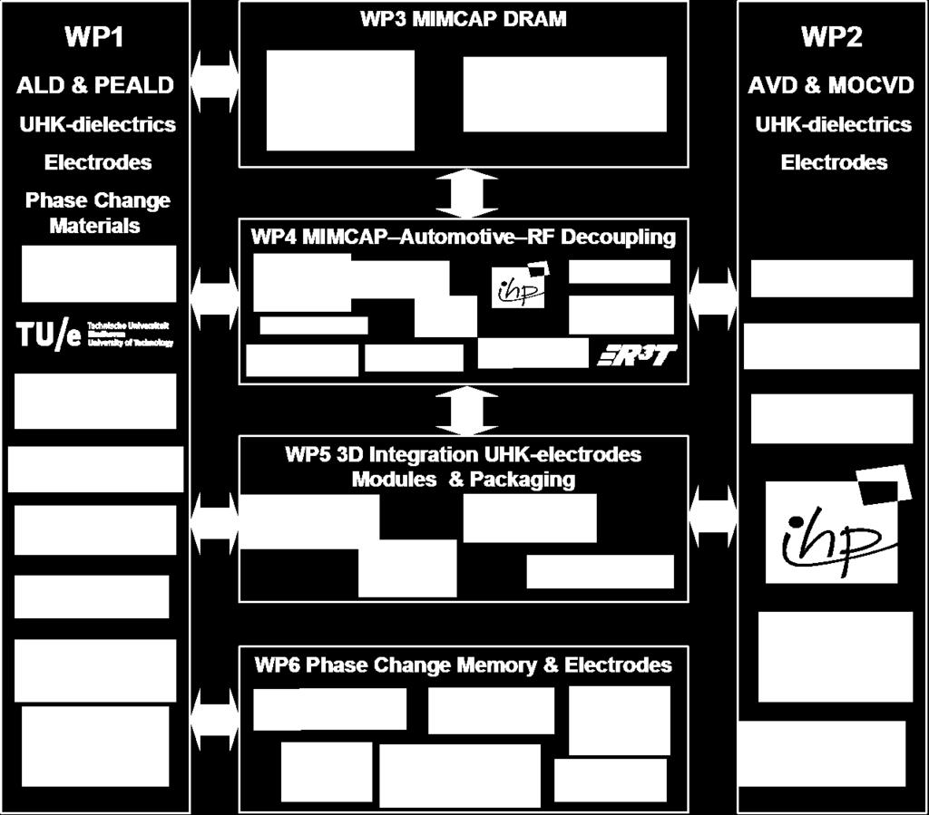
5 MaxCaps: Consortium October 11,
6 Capacitor requirements RF capacitors ITRS Roadmap 2009/2010 C f 7 J leak <10-8 A/cm² DRAM capacitors EOT J leak <10-7 A/cell October 11,
7 Capacity enhancement Capacity determined by several factors C 0 k optimization potential A d limited by trench geometry (etch process) limited by U bd /E bd October 11,
8 C f [ff/µm²] Film thickness [nm] E bd [MV/cm] Boundary conditions Specific capacity C f & film thickness determined by k J. McPherson et al., IEDM `02 Digest (2002) 633. SiO2 Al2O3 Ta2O5 ZrO2 SrTa2O6 SrTiO3 Si3N4 HfO2 La2O3 Pr2O3 TiO U bd = 15 V k Cf film thickness k October 11,
9 Dielectric material screening Target Dielectric thin film material with k >50 Film thickness up to >100 nm Excellent step coverage for trench capacitors Material screening Literature research 14 dielectric materials / material stacks evaluated 5 electrode materials evaluated Planar MIM capacitors Deposition methods AVD (MOCVD) ALD October 11,
10 J 1V [A/cm²] Dielectric material screening Leakage current 1 V J leak < 10-7 k < E E E E E E E E E E E k SrTiO/Au,Pt SrTiO/TiN,TaN PESrTiO/Au,Pt PESrTiO/TiN,TaN SrTiO&Al2O3/Au,Pt SrTiO&Al2O3/TiN,TaN SrTiO&SrTaO/Au,Pt SrTiO&SrTaO/TiN,TaN SrTiO&SrO/Au,Pt SrTiO&SrO/TiN,TaN BaSrTiO/Au,Pt BaSrTiO/TiN,TaN BaSrTiO&Al2O3/Au,Pt BaSrTiO&Al2O3/TiN,TaN BaTiO/Au,Pt BaTiO/TiN,TaN SrTaO/Au,Pt SrTaO/TiN,TaN TiTaO/Au,Pt TiTaO/TiN,TaN NbTaO/Au,Pt NbTaO/TiN,TaN AlTiO2&Al2O3/TiN,TaN CeAlO/Au,Pt CeAlO/TiN,TaN October 11,
 277. October 11, 2011 11")
11 DRAM capacitors Test device ALD SrTiO 3 /TiO x RuO x, TiN electrodes Planar device on 300 mm wafer M.A. Pawlak et al., IEEE IEDM 2010 (2010) 277. October 11,


12 DRAM capacitors J leak vs EOT M.A. Pawlak et al., IEEE IEDM 2010 (2010) 277. October 11,
13 DRAM capacitors Achievements Record low J leak = 10-6 /10-8 A/cm² at 0.4/0.5 nm EOT Low-roughness Ru oxidation process Small crystallite size of Sr-rich STO maintained by TiO x layer intermixing : high k (~85) at low J leak October 11,
14 J 3V [A/cm²] Dielectric material screening Leakage current >1 V J leak <10-7 k < E E E E E E E E E E E k SrTiO/Au,Pt SrTiO/TiN,TaN PESrTiO/Au,Pt PESrTiO/TiN,TaN SrTiO&Al2O3/Au,Pt SrTiO&Al2O3/TiN,TaN SrTiO&SrTaO/Au,Pt SrTiO&SrTaO/TiN,TaN SrTiO&SrO/Au,Pt SrTiO&SrO/TiN,TaN BaSrTiO/Au,Pt BaSrTiO/TiN,TaN BaSrTiO&Al2O3/Au,Pt BaSrTiO&Al2O3/TiN,TaN BaTiO/Au,Pt BaTiO/TiN,TaN SrTaO/Au,Pt SrTaO/TiN,TaN TiTaO/Au,Pt TiTaO/TiN,TaN NbTaO/Au,Pt NbTaO/TiN,TaN AlTiO2&Al2O3/TiN,TaN CeAlO/Au,Pt CeAlO/TiN,TaN October 11,
 5734.")
15 RF/decoupling capacitors Leakage current reduction multilayer dielectrics Crystalline SrTiO 3 high-k layer Amorphous SrTaO x leakage current blocking layer C. Baristiran Kaynak et al., Thin Solid Films 519 (2011) October 11,
16 RF/decoupling capacitors Leakage current reduction vs k eff reduction C. Baristiran Kaynak et al., Thin Solid Films 519 (2011) October 11,
17 RF/decoupling capacitors Achievements Low leakage current densities (<10-7 A/cm²) achievable only with dielectric multilayer k eff <50 Material choice: AVD BaSrTiO 3 /Al 2 O 3 & ALD SrTiO 3 /Al 2 O 3 J leak = < V k eff Voltage linearity <300 ppm/v² C f = 7.7 U bd = 15 V PDA temperature > 550 C Compatible with non-noble metal electrodes (TiN, TaN) Excellent step coverage for trench capacitors with ALD (shown for SrTiO 3, AlTiO 2 ) October 11,
 k = 29 k eff = 19 k eff = 16 HfErO x Al 2 O 3 /HfErO x /Al 2 O 3 Al 2 O 3 /HfErO x nanolaminate t diel = 80 nm Data by: B. Toomey (Analog Devices) T. Blomberg (ASM) K. Cherkaoui, S.")
18 Breakdown voltage >30 V High voltage capacitors Medium-k dielectric: ALD HfErO x (E bd = 3.9 MV/cm) Multilayers with ALD Al 2 O 3 (E bd = 7.0 MV/cm) k = 29 k eff = 19 k eff = 16 HfErO x Al 2 O 3 /HfErO x /Al 2 O 3 Al 2 O 3 /HfErO x nanolaminate t diel = 80 nm Data by: B. Toomey (Analog Devices) T. Blomberg (ASM) K. Cherkaoui, S. Monaghan (Tyndall National Insitute) October 11,
19 High voltage capacitors Achievements Nanolaminate shows lowest J leak at high k E bd Dielectric k E bd [MV/cm] k E bd J [A/cm²] HfErO x Al 2 O 3 /HfErO x /Al 2 O Al 2 O 3 /HfErO x NL Nanolaminate approach with medium-k dielectrics is a potential solution for high-voltage MIM capacitors with high capacitance density Optimization ongoing October 11,
20 Summary Extensive material screening performed Leakage current density limited choice of high-k dielectric depends on operating voltage DRAM capacitors k 100 RF/decoupling capacitors k <50 High voltage capacitors k <20 Deposition processes available Planar & moderate AR trench capacitors AVD & ALD High AR trench capacitors ALD MaxCaps is a joint success of cooperating partners along the whole value chain October 11,
3D Stacked Buck Converter with SrTiO 3 (STO) Capacitors on Silicon Interposer
 Capacitors on Silicon Interposer") 3D Stacked Buck Converter with SrTiO 3 (STO) Capacitors on Silicon Interposer Makoto Takamiya 1, Koichi Ishida 1, Koichi Takemura 2,3, and Takayasu Sakurai 1 1 University of Tokyo, Japan 2 NEC Corporation,
3D Stacked Buck Converter with SrTiO 3 (STO) Capacitors on Silicon Interposer Makoto Takamiya 1, Koichi Ishida 1, Koichi Takemura 2,3, and Takayasu Sakurai 1 1 University of Tokyo, Japan 2 NEC Corporation,
Agenda. 1. Atomic Layer Deposition Technology
 Agenda 1. Atomic Layer Deposition Technology 2. What is ALD? Atomic Layer Deposition is invented in 1977 by T. Suntola et al. - New Deposition Method for Electro-Luminescent Display (ZnS:Mn Thin Films)
PROGRESS AND ISSUES IN DIELECTRIC MATERIALS FOR SUB-100NM DRAM TECHNOLOGY ABSTRACT
 PROGRESS AND ISSUES IN DIELECTRIC MATERIALS FOR SUB-100NM DRAM TECHNOLOGY Kanta Saino Device Integration Group, Technology & Development Office, Elpida Memory Inc. 7-10 Yoshikawakogyodanchi, Higashihiroshima,
Low leakage ZrO 2 based capacitors for sub 20 nm DRAM technology nodes
 Low leakage ZrO 2 based capacitors for sub 20 nm DRAM technology nodes Milan Pešić, 1 Steve Knebel, 1 Maximilian Geyer, 1 Sebastian Schmelzer 2, Ulrich Böttger 2, Nadiia Kolomiiets 3, Valeri V. Afanas
RECENTLY, (Ba, Sr)TiO thin films have been intensively
TiO thin films have been intensively") 342 IEEE TRANSACTIONS ON ELECTRON DEVICES, VOL. 46, NO. 2, FEBRUARY 1999 Impact of Time Dependent Dielectric Breakdown and Stress-Induced Leakage Current on the Reliability of High Dielectric Constant
342 IEEE TRANSACTIONS ON ELECTRON DEVICES, VOL. 46, NO. 2, FEBRUARY 1999 Impact of Time Dependent Dielectric Breakdown and Stress-Induced Leakage Current on the Reliability of High Dielectric Constant
Alternative deposition solution for cost reduction of TSV integration
 Alternative deposition solution for cost reduction of TSV integration J. Vitiello, F. Piallat, L. Bonnet KOBUS 611 rue Aristide Bergès, Z.A. de Pré Millet, Montbonnot-Saint-Martin, 38330 France Ph: +33
ALD deposited ferroelectric HfO 2
 ALD deposited ferroelectric HfO 2 S. Slesazeck 1, U. Schroeder 1, E. Yurchuk 1, J. Müller 2, S. Müller 1, D. Martin 1, T. Schenk 1, C. Richter 1,C. Adelmann 3, S. Kalinin 5, A. Kersch 7, and T. Mikolajick
Jusung Engineering, Korea and France
 First Int. Workshop on Power Supply On Chip (PowerSoC08), Sept. 22-24, 2008, Cork, Ireland Ultrahigh-density (> 0.4 µf/mm 2 ) trench capacitors in silicon F. Roozeboom 1,2, W. Dekkers 1, K. Jinesh 1, W.
MODELING OF CV CHARACTERISTICS OF HIGH-k MIM CAPACITORS
 Chapter 6 MODELING OF CV CHARACTERISTICS OF HIGH-k MIM CAPACITORS 6.1 Introduction and Motivation Capacitance-Voltage characteristics and voltage linearity of MIM capacitor are important performance parameters
EE 292L : Nanomanufacturing. Week 5: Advanced Process Technology. Oct
 EE 292L : Nanomanufacturing Week 5: Advanced Process Technology Oct 22 2012 1 Advanced Process Technology 1 HAR etch 2 3 HAR Gapfill Metal ALD 4 Reflow 5 6 SAC Airgap 7 8 Strain Ge/III-V Engineering 1
Moores Law for DRAM. 2x increase in capacity every 18 months 2006: 4GB
 MEMORY Moores Law for DRAM 2x increase in capacity every 18 months 2006: 4GB Corollary to Moores Law Cost / chip ~ constant (packaging) Cost / bit = 2X reduction / 18 months Current (2008) ~ 1 micro-cent
Effective Capacitance Enhancement Methods for 90-nm DRAM Capacitors
 Journal of the Korean Physical Society, Vol. 44, No. 1, January 2004, pp. 112 116 Effective Capacitance Enhancement Methods for 90-nm DRAM Capacitors Y. K. Park, Y. S. Ahn, S. B. Kim, K. H. Lee, C. H.
Influence of electrode materials on CeO x based resistive switching
 Influence of electrode materials on CeO x based resistive switching S. Kano a, C. Dou a, M. Hadi a, K. Kakushima b, P. Ahmet a, A. Nishiyama b, N. Sugii b, K. Tsutsui b, Y. Kataoka b, K. Natori a, E. Miranda
FIB Voltage Contrast for Failure Localisation on CMOS Circuits an Overview
 for Failure Localisation on CMOS Circuits an Overview 8th European FIB User Group Meeting Zürich 2004 Dr. rer. nat. Rüdiger Rosenkranz Infineon Technologies Dresden Physical Failure Analysis Page 1 Never
CVD: General considerations.
 CVD: General considerations. PVD: Move material from bulk to thin film form. Limited primarily to metals or simple materials. Limited by thermal stability/vapor pressure considerations. Typically requires
Frequency dispersion effect and parameters. extraction method for novel HfO 2 as gate dielectric
 048 SCIENCE CHINA Information Sciences April 2010 Vol. 53 No. 4: 878 884 doi: 10.1007/s11432-010-0079-8 Frequency dispersion effect and parameters extraction method for novel HfO 2 as gate dielectric LIU
Ferroelectric HfO 2 Thin Films
 Ferroelectric HfO 2 Thin Films May 12 th, 2015 JACKSON ANDERSON ELECTRICAL AND MICROELECTRONIC ENGINEERING ROCHESTER INSTITUTE OF TECHNOLOGY Outline Introduction Background Project Objectives Experimental
Objective: Competitive Low-Cost Thin-Film Varactor Technology. Integrated Monolithic Capacitors using Sputtered/MOCVD material on low-cost substrates
 Overview of Program Objective: Competitive Low-Cost Thin-Film Varactor Technology coplanar waveguide (CPW) capacitor ground signal ground Si substrate etched troughs Focus of Our Program! Reproducibility!
Steep-slope WSe 2 Negative Capacitance Field-effect Transistor
 Supplementary Information for: Steep-slope WSe 2 Negative Capacitance Field-effect Transistor Mengwei Si, Chunsheng Jiang, Wonil Chung, Yuchen Du, Muhammad A. Alam, and Peide D. Ye School of Electrical
Thin Film Transistors (TFT)
") Thin Film Transistors (TFT) a-si TFT - α-si:h (Hydrogenated amorphous Si) deposited with a PECVD system (low temp. process) replaces the single crystal Si substrate. - Inverted staggered structure with
Thin Film Transistors (TFT) a-si TFT - α-si:h (Hydrogenated amorphous Si) deposited with a PECVD system (low temp. process) replaces the single crystal Si substrate. - Inverted staggered structure with
3D capacitors on silicon with high density pore network and ZrO2 dielectric films deposited by MOCVD
 3D capacitors on silicon with high density pore network and ZrO2 dielectric films deposited by MOCVD Magali Brunet 1, Gérald Leclerc 1, Emmanuel Scheid 1, Jean- Louis Sanchez 1 1 LAAS-CNRS, University
Analysis of Band-to-band. Tunneling Structures. Title of Talk. Dimitri Antoniadis and Judy Hoyt (PIs) Jamie Teherani and Tao Yu (Students) 8/21/2012
 Jamie Teherani and Tao Yu (Students) 8/21/2012") 1 Analysis of Band-to-band Title of Talk Tunneling Structures Dimitri Antoniadis and Judy Hoyt (PIs) Jamie Teherani and Tao Yu (Students) 8/21/2012 A Science & Technology Center Vertical Type-II TFET Structure
1 Analysis of Band-to-band Title of Talk Tunneling Structures Dimitri Antoniadis and Judy Hoyt (PIs) Jamie Teherani and Tao Yu (Students) 8/21/2012 A Science & Technology Center Vertical Type-II TFET Structure
Aerospace Performances of IPDiA -250 C up to 250 C Grade Silicon Capacitors
 Aerospace Performances of IPDiA -250 C up to 250 C Grade Silicon Capacitors Laurent Lengignon, IPDiA, 2 rue de la Girafe, 14000 Caen, France Alter Technology, Madrid, Spain, Demetrio Lopez ESA/ESTEC, Noordwijk,
+ V gate M O. Trend: As k, E g. Part 6: High Dielectric Constant (k), Gate Electrode, & Channel Materials. Bandgap versus Dielectric Constant (k) k k
, Gate Electrode, & Channel Materials. Bandgap versus Dielectric Constant (k) k k") Part 6: High Dielectric Constant (k), Gate Electrode, & Channel Materials O 2 gate oxide is approaching physical limits Thickness & Current M O S poly-crystalline V Source W Source Contact Insulator n
Part 6: High Dielectric Constant (k), Gate Electrode, & Channel Materials O 2 gate oxide is approaching physical limits Thickness & Current M O S poly-crystalline V Source W Source Contact Insulator n
Quantum Mechanical Simulation for Ultra-thin High-k Gate Dielectrics Metal Oxide Semiconductor Field Effect Transistors
 Mechanical Simulation for Ultra-thin High-k Gate Dielectrics Metal Oxide Semiconductor Field Effect Transistors Shih-Ching Lo 1, Yiming Li 2,3, and Jyun-Hwei Tsai 1 1 National Center for High-Performance
Inductive crystallization effect of atomic-layerdeposited
 Zhang et al. Nanoscale Research Letters (2015) 10:25 DOI 10.1186/s11671-014-0711-4 NANO EXPRESS Open Access Inductive crystallization effect of atomic-layerdeposited Hf 0.5 Zr 0.5 O 2 films for ferroelectric
Control of Flat Band Voltage by Partial Incorporation of La 2 O 3 or Sc 2 O 3 into HfO 2 in Metal/HfO 2 /SiO 2 /Si MOS Capacitors
 Control of Flat Band Voltage by Partial Incorporation of La 2 O 3 or Sc 2 O 3 into HfO 2 in Metal/HfO 2 /SiO 2 /Si MOS Capacitors M. Adachi 1, K. Okamoto 1, K. Kakushima 2, P. Ahmet 1, K. Tsutsui 2, N.
Electrical and Reliability Characteristics of RRAM for Cross-point Memory Applications. Hyunsang Hwang
 Electrical and Reliability Characteristics of RRAM for Cross-point Memory Applications Hyunsang Hwang Dept. of Materials Science and Engineering Gwangju Institute of Science and Technology (GIST), KOREA
Experimental and Theoretical Study of Electrode Effects in HfO2 based RRAM
 Experimental and Theoretical Study of Electrode Effects in HfO2 based RRAM C. Cagli 1, J. Buckley 1, V. Jousseaume 1, T. Cabout 1, A. Salaun 1, H. Grampeix 1, J. F. Nodin 1,H. Feldis 1, A. Persico 1, J.
Abstract. Metal-insulator-metal (MIM) capacitors comprised of amorphous Si:SrTiO 3 -Al 2 O 3 -Si:SrTiO 3
 capacitors comprised of amorphous Si:SrTiO 3 -Al 2 O 3 -Si:SrTiO 3") Si:SrTiO 3 -Al 2 O 3 -Si:SrTiO 3 multi-dielectric architecture for metal-insulatormetal capacitor applications Sita Dugu 1, Shojan P. Pavunny 1*, James F. Scott 1,2, and Ram S. Katiyar 1 * 1 Department
Si:SrTiO 3 -Al 2 O 3 -Si:SrTiO 3 multi-dielectric architecture for metal-insulatormetal capacitor applications Sita Dugu 1, Shojan P. Pavunny 1*, James F. Scott 1,2, and Ram S. Katiyar 1 * 1 Department
High Dielectric Constant (k) Materials
 Materials") Part 6: High Dielectric Constant (k), Gate Electrode, & Channel Materials O 2 gate ide is approaching physical limits Thickness & Current M O S poly-crystalline V Source W Source Contact Insulator n +
Part 6: High Dielectric Constant (k), Gate Electrode, & Channel Materials O 2 gate ide is approaching physical limits Thickness & Current M O S poly-crystalline V Source W Source Contact Insulator n +
The Pennsylvania State University. Kurt J. Lesker Company. North Carolina State University. Taiwan Semiconductor Manufacturing Company 1
 Enhancement Mode Strained (1.3%) Germanium Quantum Well FinFET (W fin =20nm) with High Mobility (μ Hole =700 cm 2 /Vs), Low EOT (~0.7nm) on Bulk Silicon Substrate A. Agrawal 1, M. Barth 1, G. B. Rayner
Plasma Deposition (Overview) Lecture 1
 Lecture 1") Plasma Deposition (Overview) Lecture 1 Material Processes Plasma Processing Plasma-assisted Deposition Implantation Surface Modification Development of Plasma-based processing Microelectronics needs (fabrication
Plasma Deposition (Overview) Lecture 1 Material Processes Plasma Processing Plasma-assisted Deposition Implantation Surface Modification Development of Plasma-based processing Microelectronics needs (fabrication
Atomic Layer Deposition: An Enabling Technology for Microelectronic Device Manufacturing
 Atomic Layer Deposition: An Enabling Technology for Microelectronic Device Manufacturing Fourmun Lee*, Steve Marcus, Eric Shero, Glen Wilk Johan Swerts, Jan Willem Maes, Tom Blomberg ASM America Inc.,
Chapter 13. Capacitors
 Chapter 13 Capacitors Objectives Describe the basic structure and characteristics of a capacitor Discuss various types of capacitors Analyze series capacitors Analyze parallel capacitors Analyze capacitive
Challenges and Opportunities. Prof. J. Raynien Kwo 年
 Nanoelectronics Beyond Si: Challenges and Opportunities Prof. J. Raynien Kwo 年 立 Si CMOS Device Scaling Beyond 22 nm node High κ,, Metal gates, and High mobility channel 1947 First Transistor 1960 1960
Hotwire-assisted Atomic Layer Deposition of Pure Metals and Metal Nitrides
 Hotwire-assisted Atomic Layer Deposition of Pure Metals and Metal Nitrides Alexey Kovalgin MESA+ Institute for Nanotechnology Semiconductor Components group a.y.kovalgin@utwente.nl 1 Motivation 1. Materials
JOHN G. EKERDT RESEARCH FOCUS
 JOHN G. EKERDT RESEARCH FOCUS We study the surface, growth and materials chemistry of metal, dielectric, ferroelectric, and polymer thin films. We seek to understand and describe nucleation and growth
CVD-3 LFSIN SiN x Process
 CVD-3 LFSIN SiN x Process Top Electrode, C Bottom Electrode, C Pump to Base Time (s) SiH 4 Flow Standard LFSIN Process NH 3 Flow N 2 HF (watts) LF (watts) Pressure (mtorr Deposition Time min:s.s Pump to
N ano scale l S il ii lco i n B ased N o nvo lat l i atl ie l M em ory r Chungwoo Kim, Ph.D.
 cw_kim@samsung.com Acknowledgements Collaboration Funding Outline Introduction Current research status Nano fabrication Process Nanoscale patterning SiN thin film Si Nanoparticle Nano devices Nanoscale
The goal of this project is to enhance the power density and lowtemperature efficiency of solid oxide fuel cells (SOFC) manufactured by atomic layer
 manufactured by atomic layer") Stanford University Michael Shandalov1, Shriram Ramanathan2, Changhyun Ko2 and Paul McIntyre1 1Department of Materials Science and Engineering, Stanford University 2Division of Engineering and Applied
Stanford University Michael Shandalov1, Shriram Ramanathan2, Changhyun Ko2 and Paul McIntyre1 1Department of Materials Science and Engineering, Stanford University 2Division of Engineering and Applied
CVD-3 SIO-HU SiO 2 Process
 CVD-3 SIO-HU SiO 2 Process Top Electrode, C Bottom Electrode, C Pump to Base Time (s) SiH 4 Flow Standard SIO-HU Process N 2 O Flow N 2 HF (watts) LF (watts) Pressure (mtorr Deposition Time min:s.s Pump
An interfacial investigation of high-dielectric constant material hafnium oxide on Si substrate B
 Thin Solid Films 488 (2005) 167 172 www.elsevier.com/locate/tsf An interfacial investigation of high-dielectric constant material hafnium oxide on Si substrate B S.C. Chen a, T, J.C. Lou a, C.H. Chien
R&D Issues for High-k Gate Dielectrics
 R&D Issues for High-k Gate Dielectrics T.P. Ma Yale University Spacer High-k Gate Dielectric Stack Source Drain Gate electrode, poly Upper interfacial region Bulk high-k film Lower interfacial region Substrate
Laboratoire L2MP 14 janvier 2005
 Assemblée e Générale G L2MP 14 janvier 2005 A highly reliable 3-dimensional integrated SBT ferroelectric capacitor enabling FeRAM scaling L2MP (France) N. Menou (PhD), V. Madigou,, Ch. Turquat, D. Goguenheim,,
Benefits of Stacked-Wafer Capacitors for High-Frequency Buck Converters
 Benefits of Stacked-Wafer Capacitors for High-Frequency Buck Converters Michael W. Baker, PhD Maxim Integrated Power SoC Northeastern University, Boston MA. October 7, 2014 Mobile Device Trends Power Management
Chapter 1. Introduction
 Chapter 1. Introduction In this chapter, ferroelectric materials are briefly introduced with emphasis on their nonvolatile memory properties and their potential impact on the current state of digital memories.
Extrinsic and Intrinsic Frequency Dispersion of High-k Materials in Capacitance-Voltage Measurements
 Materials 01, 5, 1005-103; doi:10.3390/ma5061005 Review OPEN ACCESS materials ISSN 1996-1944 www.mdpi.com/journal/materials Extrinsic and Intrinsic Frequency Dispersion of High-k Materials in Capacitance-Voltage
Comparative studies of Ge and Si p-channel metal oxide semiconductor field-effect-transistors with HfSiON dielectric and TaN metal gate
 Comparative studies of Ge and Si p-channel metal oxide semiconductor field-effect-transistors with HfSiON dielectric and TaN metal gate Hu Ai-Bin( 胡爱斌 ) and Xu Qiu-Xia( 徐秋霞 ) Institute of Microelectronics,
Electronics with 2D Crystals: Scaling extender, or harbinger of new functions?
 Electronics with 2D Crystals: Scaling extender, or harbinger of new functions? 1 st Workshop on Data Abundant Systems Technology Stanford, April 2014 Debdeep Jena (djena@nd.edu) Electrical Engineering,
Enhanced Mobility CMOS
 Enhanced Mobility CMOS Judy L. Hoyt I. Åberg, C. Ni Chléirigh, O. Olubuyide, J. Jung, S. Yu, E.A. Fitzgerald, and D.A. Antoniadis Microsystems Technology Laboratory MIT, Cambridge, MA 02139 Acknowledge
Emerging Applications for High K Materials in VLSI Technology
 Materials 2014, 7, 2913-2944; doi:10.3390/ma7042913 Review OPEN ACCESS materials ISSN 1996-1944 www.mdpi.com/journal/materials Emerging Applications for High K Materials in VLSI Technology Robert D. Clark
Characterization of Charge Trapping and Dielectric Breakdown of HfAlOx/SiON Dielectric Gate Stack
 Characterization of Charge Trapping and Dielectric Breakdown of HfAlOx/SiON Dielectric Gate Stack Y. Pei, S. Nagamachi, H. Murakami, S. Higashi, S. Miyazaki, T. Kawahara and K. Torii Graduate School of
Chapt ha e pt r e r 9 Capacitors
 Chapter 9 Capacitors Basics of a Capacitor In its simplest form, a capacitor is an electrical device constructed of two parallel plates separated by an insulating material called the dielectric In the
CVD-3 MFSIN-HU-2 SiN x Mixed Frequency Process
 CVD-3 MFSIN-HU-2 SiN x Mixed Frequency Process Standard MFSIN-HU-2 Process Top C Bottom C Pump to Base Time (s) SiH 4 Flow HF/ LF NH 3 Flow HF/LF N 2 HF/LF HF (watts) LF (watts) HF Time LF Time Pressure
A final review session will be offered on Thursday, May 10 from 10AM to 12noon in 521 Cory (the Hogan Room).
.") A final review session will be offered on Thursday, May 10 from 10AM to 12noon in 521 Cory (the Hogan Room). The Final Exam will take place from 12:30PM to 3:30PM on Saturday May 12 in 60 Evans.» All of
A final review session will be offered on Thursday, May 10 from 10AM to 12noon in 521 Cory (the Hogan Room). The Final Exam will take place from 12:30PM to 3:30PM on Saturday May 12 in 60 Evans.» All of
Automotive Grade Silicon Capacitors for Under the Hood Applications
 Automotive Grade Silicon Capacitors for Under the Hood Applications Sébastien Jacqueline, Laurent Lengignon, Laëtitia Omnès IPDiA, 2 rue de la Girafe, 14000 Caen, France laetitia.omnes@ipdia.com, +33 (0)
CVD-3 MFSIN-HU-1 SiN x Mixed Frequency Process
 CVD-3 MFSIN-HU-1 SiN x Mixed Frequency Process Standard MFSIN-HU-1 Process Top C Bottom C Pump to Base Time (s) SiH 4 Flow HF/ LF NH 3 Flow HF/LF N 2 HF/LF HF (watts) LF (watts) HF Time LF Time Pressure
DEPOSITION OF THIN TiO 2 FILMS BY DC MAGNETRON SPUTTERING METHOD
 Chapter 4 DEPOSITION OF THIN TiO 2 FILMS BY DC MAGNETRON SPUTTERING METHOD 4.1 INTRODUCTION Sputter deposition process is another old technique being used in modern semiconductor industries. Sputtering
ALD high-k and higher-k integration on GaAs
 ALD high-k and higher-k integration on GaAs Ozhan Koybasi 1), Min Xu 1), Yiqun Liu 2), Jun-Jieh Wang 2), Roy G. Gordon 2), and Peide D. Ye 1)* 1) School of Electrical and Computer Engineering, Purdue University,
Scaling up Chemical Vapor Deposition Graphene to 300 mm Si substrates
 Scaling up Chemical Vapor Deposition Graphene to 300 mm Si substrates Co- Authors Aixtron Alex Jouvray Simon Buttress Gavin Dodge Ken Teo The work shown here has received partial funding from the European
SCALE-UP OF THE BARIUM TITANATE ATOMIC LAYER DEPOSITION PROCESS ONTO 200 MM WAFER
 1.1149/1.229339, copyright The Electrochemical Society SCALE-UP OF THE BARIUM TITANATE ATOMIC LAYER DEPOSITION PROCESS ONTO 2 MM WAFER R. Matero, A. Rahtu, S. Haukka, M. Tuominen, M. Vehkamäki 1, T. Hatanpää
Improved Interfacial and Electrical Properties of GaSb Metal Oxide
 Improved Interfacial and Electrical Properties of GaSb Metal Oxide Semiconductor Devices Passivated with Acidic (NH 4 ) 2 S Solution Lianfeng Zhao, Zhen Tan, Jing Wang, and Jun Xu * Tsinghua National Laboratory
ALD & ALE Tutorial Speakers and Schedule
 ALD & ALE Tutorial Speakers and Schedule Sunday, July 29, 2018 1:00-1:05 Tutorial Welcome 1:05-1:50 1:50-2:35 2:35-3:20 Challenges of ALD Applications in Memory Semiconductor Devices, Choon Hwan Kim (SK
Random Access Memory. DRAM & SRAM Design DRAM SRAM MS635. Dynamic Random Access Memory. Static Random Access Memory. Cell Structure. 6 Tr.
 DRAM & SRAM Design Random Access Memory Volatile memory Random access is possible if you know the address DRAM DRAM Dynamic Random Access Memory SRAM Static Random Access Memory SRAM Cell Structure Power
MICROCHIP MANUFACTURING by S. Wolf
 by S. Wolf Chapter 15 ALUMINUM THIN-FILMS and SPUTTER-DEPOSITION 2004 by LATTICE PRESS CHAPTER 15 - CONTENTS Aluminum Thin-Films Sputter-Deposition Process Steps Physics of Sputter-Deposition Magnetron-Sputtering
Gold Nanoparticles Floating Gate MISFET for Non-Volatile Memory Applications
 Gold Nanoparticles Floating Gate MISFET for Non-Volatile Memory Applications D. Tsoukalas, S. Kolliopoulou, P. Dimitrakis, P. Normand Institute of Microelectronics, NCSR Demokritos, Athens, Greece S. Paul,
2DFUN - 2D FUNCTIONAL MX 2 /GRAPHENE HETERO-STRUCTURES
 www.2dfun.eu 2DFUN - 2D FUNCTIONAL MX 2 /GRAPHENE HETERO-STRUCTURES FLAG-ERA JTC 2015 PROJECT KICK-OFF APRIL 13, 2016, BUDAPEST, HUNGARY, PROJECT COORDINATOR 2D MATERIALS GRAPHENE AND BEYOND VISION AND
Graphene Varactors as a Sensing Platform for Biotechnology Applications
 Graphene Varactors as a Sensing Platform for Biotechnology Applications Steven J. Koester 1, Eric J. Olson 1, David Deen 1, Yao Zhang 1, Mona A. Ebrish 1, Rui Ma 1, Nazila Haratipour 1, Philippe Buhlmann
Three-dimensional AlZnO/Al 2 O 3 /AlZnO nanocapacitor arrays on Si substrate for energy storage
 Li et al. Nanoscale Research Letters 2012, 7:544 NANO EXPRESS Three-dimensional AlZnO/Al 2 O 3 /AlZnO nanocapacitor arrays on Si substrate for energy storage Lian-Jie Li 1, Bao Zhu 1, Shi-Jin Ding 1*,
Mechanism of Switching and Related Challenges in Transition Metal Oxide Based RRAM Devices
 Mechanism of Switching and Related Challenges in Transition Metal Oxide Based RRAM Devices Rashmi Jha and Branden Long Dept. of Electrical Engineering and Computer Science University of Toledo Toledo,
SPUTTER DEPOSITION PROCESSES FOR THIN FILM OXIDE DIELECTRICS
 SPUTTER DEPOSITION PROCESSES FOR THIN FILM OXIDE DIELECTRICS A Dissertation Presented to the Faculty of the Graduate School of Cornell University in Partial Fulfillment of the Requirements for the Degree
Modeling of Leakage Currents in High-κ Dielectrics
 TECHNISCHE UNIVERSITÄT MÜNCHEN Institut für Nanoelektronik Modeling of Leakage Currents in High-κ Dielectrics Gunther Christian Jegert Vollständiger Abdruck der von der Fakultät für Elektrotechnik und
Nanofabrication Lab Process Development for High-k Dielectrics
 Nanofabrication Lab Process Development for Highk Dielectrics Each lab group consists of 4 to 5 students. The dates of these Labs are: Lab 1 Date 14.02.2013 Time: 812 am Lab 2 Date 14.02.2013 Time: 15
Size-dependent Metal-insulator Transition Random Materials Crystalline & Amorphous Purely Electronic Switching
 Nanometallic RRAM I-Wei Chen Department of Materials Science and Engineering University of Pennsylvania Philadelphia, PA 19104 Nature Nano, 6, 237 (2011) Adv Mater,, 23, 3847 (2011) Adv Func Mater,, 22,
New Ferroelectric Material for Embedded FRAM LSIs
 New Ferroelectric Material for Embedded FRAM LSIs V Kenji Maruyama V Masao Kondo V Sushil K. Singh V Hiroshi Ishiwara (Manuscript received April 5, 2007) The strong growth of information network infrastructures
There s Plenty of Room at the Bottom and at the Top
 14 nm chip X SEM from www.intel.com/content/dam/www/public/us/en/documents/pdf/foundry/mark bohr 2014 idf presentation.pdf There s Plenty of Room at the Bottom and at the Top Tsu Jae King Liu Department
A Novel Approach to TSV Metallization based on Electrografted Copper Nucleation Layers. Claudio Truzzi, PhD Chief Technology Officer Alchimer
 A Novel Approach to TSV Metallization based on Electrografted Copper Nucleation Layers Claudio Truzzi, PhD Chief Technology Officer Alchimer Overview Introduction Electrografting (eg) Technology Description
Technology Brief 9: Capacitive Sensors
 218 TEHNOLOGY BRIEF 9: APAITIVE SENSORS Technology Brief 9: apacitive Sensors To sense is to respond to a stimulus. (See Tech Brief 7 on resistive sensors.) A capacitor can function as a sensor if the
Homework #1 - September 9, Due: September 16, 2005 at recitation ( 2 PM latest) (late homework will not be accepted)
 (late homework will not be accepted)") Fall 2005 6.012 Microelectronic Devices and Circuits Prof. J. A. del Alamo Homework #1 - September 9, 2005 Due: September 16, 2005 at recitation ( 2 PM latest) (late homework will not be accepted) Please
Fall 2005 6.012 Microelectronic Devices and Circuits Prof. J. A. del Alamo Homework #1 - September 9, 2005 Due: September 16, 2005 at recitation ( 2 PM latest) (late homework will not be accepted) Please
Chapter 20 Electric Potential and Electric Potential Energy
 Chapter 20 Electric Potential and Electric Potential Energy 1 Overview of Chapter 20 Electric Potential Energy and the Electric Potential! Energy Conservation! The Electric Potential of Point Charges!
Suppression of Gate-Induced Drain Leakage by Optimization of Junction Profiles in 22 nm and 32 nm SOI nfets
 Suppression of Gate-Induced Drain Leakage by Optimization of Junction Profiles in 22 nm and 32 nm SOI nfets Andreas Schenk a,, a Integrated Systems Laboratory, ETH Zurich, Gloriastrasse 35, CH-8092, Switzerland
USOO A United States Patent (19) 11 Patent Number: 5,923,062 Ohno (45) Date of Patent: *Jul. 13, 1999
 11 Patent Number: 5,923,062 Ohno (45) Date of Patent: *Jul. 13, 1999") USOO5923062A United States Patent (19) 11 Patent Number: 5,923,062 Ohno (45) Date of Patent: *Jul. 13, 1999 54 SEMICONDUCTOR DEVICE 5,559,666 9/1996 Figura et al.. NCORPORATING CAPACTORS 5,568,352 10/1996
USOO5923062A United States Patent (19) 11 Patent Number: 5,923,062 Ohno (45) Date of Patent: *Jul. 13, 1999 54 SEMICONDUCTOR DEVICE 5,559,666 9/1996 Figura et al.. NCORPORATING CAPACTORS 5,568,352 10/1996
JOHN G. EKERDT RESEARCH FOCUS
 JOHN G. EKERDT RESEARCH FOCUS We study the surface, growth and materials chemistry of ultrathin metal and dielectric films. Our work seeks to: 1) develop and understand the reactions and chemistry that
Carbon Nanotubes for Interconnect Applications Franz Kreupl, Andrew P. Graham, Maik Liebau, Georg S. Duesberg, Robert Seidel, Eugen Unger
 Carbon Nanotubes for Interconnect Applications Franz Kreupl, Andrew P. Graham, Maik Liebau, Georg S. Duesberg, Robert Seidel, Eugen Unger Infineon Technologies Corporate Research Munich, Germany Outline
Manufacture of Nanostructures for Power Electronics Applications
 Manufacture of Nanostructures for Power Electronics Applications Brian Hunt and Jon Lai Etamota Corporation 2672 E. Walnut St. Pasadena, CA 91107 APEC, Palm Springs Feb. 23rd, 2010 1 Background Outline
in this web service Cambridge University Press
 High-k Materials Mat. Res. Soc. Symp. Proc. Vol. 670 2001 Materials Research Society Materials and Physical Properties of Novel High-k and Medium-k Gate Dielectrics Ran Liu, Stefan Zollner, Peter Fejes,
Multiple Gate CMOS and Beyond
 Multiple CMOS and Beyond Dept. of EECS, KAIST Yang-Kyu Choi Outline 1. Ultimate Scaling of MOSFETs - 3nm Nanowire FET - 8nm Non-Volatile Memory Device 2. Multiple Functions of MOSFETs 3. Summary 2 CMOS
This presentation will describe my research here during SULI s summer 2012 program. My project was to fabricate nano-film capacitors.
 This presentation will describe my research here during SULI s summer 2012 program. My project was to fabricate nano-film capacitors. I was given this project because the Linac Coherent Light Source s
Reliability and Instability of GaN MIS-HEMTs for Power Electronics
 Reliability and Instability of GaN MIS-HEMTs for Power Electronics Jesús A. del Alamo, Alex Guo and Shireen Warnock Microsystems Technology Laboratories Massachusetts Institute of Technology 2016 Fall
Atomic layer deposition of titanium nitride
 Atomic layer deposition of titanium nitride Jue Yue,version4, 04/26/2015 Introduction Titanium nitride is a hard and metallic material which has found many applications, e.g.as a wear resistant coating[1],
Film Deposition Part 1
 1 Film Deposition Part 1 Chapter 11 : Semiconductor Manufacturing Technology by M. Quirk & J. Serda Spring Semester 2013 Saroj Kumar Patra Semidonductor Manufacturing Technology, Norwegian University of
TECHCET s Review of Sematech s Surface Preparation & Cleaning Conference Saratoga Springs, NY, May 12-14, 2015 Part 1 of 2
 TECHCET s Review of Sematech s Surface Preparation & Cleaning Conference Saratoga Springs, NY, May 12-14, 2015 Part 1 of 2 Presentations from SPCC related to the latest Wet Cleaning / Etching / Surface
Jiro Yota. GaAs Technology, Skyworks Solutions, Inc W. Hillcrest Drive, Newbury Park, CA 91320, USA
 ALD HfO 2 and Al 2 O 3 as MIM Capacitor Dielectric for GaAs HBT Technology Jiro Yota GaAs Technology, Skyworks Solutions, Inc. 2427 W. Hillcrest Drive, Newbury Park, CA 91320, USA jiro.yota@skyworksinc.com
J. Price, 1,2 Y. Q. An, 1 M. C. Downer 1 1 The university of Texas at Austin, Department of Physics, Austin, TX
 Understanding process-dependent oxygen vacancies in thin HfO 2 /SiO 2 stacked-films on Si (100) via competing electron-hole injection dynamic contributions to second harmonic generation. J. Price, 1,2
ABSTRACT INTRODUCTION
 CHEMICAL VAPOR DEPOSITION OF ZIRCONIUM TIN TITANATE: A DIELECTRIC MATERIAL FOR POTENTIAL MICROELECTRONIC APPLICATIONS Ebony L. Mays 1, 4, Dennis W. Hess 2 1, 3, 4, and William S. Rees, Jr. Departments
Master Thesis. Effect of Alkali-earth-elements Incorporation on La 2 O 3 Dielectrics for Scaled Silicon MOS Device
 Master Thesis Effect of Alkali-earth-elements Incorporation on Dielectrics for Scaled Silicon MOS Device Tomotsune Koyanagi Department of Electronics and Applied Physics Interdisciplinary Graduate School
FLCC Seminar. Spacer Lithography for Reduced Variability in MOSFET Performance
 1 Seminar Spacer Lithography for Reduced Variability in MOSFET Performance Prof. Tsu-Jae King Liu Electrical Engineering & Computer Sciences Dept. University of California at Berkeley Graduate Student:
Capacitors. Charging a Capacitor. Charge and Capacitance. L05: Capacitors and Inductors
 L05: Capacitors and Inductors 50 Capacitors 51 Outline of the lecture: Capacitors and capacitance. Energy storage. Capacitance formula. Types of capacitors. Inductors and inductance. Inductance formula.
Al-Doped TiO 2 Films with Ultralow Leakage Currents for Next Generation DRAM Capacitors**
 DOI: 10.1002/adma.200701085 Al-Doped TiO 2 Films with Ultralow Leakage Currents for Next Generation DRAM Capacitors** By Seong Keun Kim, Gyu-Jin Choi, Sang Young Lee, Minha Seo, Sang Woon Lee, Jeong Hwan