Size-dependent Metal-insulator Transition Random Materials Crystalline & Amorphous Purely Electronic Switching
|
|
|
- Constance Lamb
- 6 years ago
- Views:
Transcription
1 Nanometallic RRAM I-Wei Chen Department of Materials Science and Engineering University of Pennsylvania Philadelphia, PA Nature Nano, 6, 237 (2011) Adv Mater,, 23, 3847 (2011) Adv Func Mater,, 22, 546 (2012)
2 Size-dependent Metal-insulator Transition Random Materials Crystalline & Amorphous Purely Electronic Switching
3 A Metal? An Insulator?
4 Periodic System With a band gap, or without Insulator: : infinite resistivity at 0K Metal: : finite resistivity at 0K
5 Random System Aperiodic: No sharp band edge Mott : Mobility edge (k space) Anderson: = diffusion i 0K (elastic tunneling) = extent of wave function Metallic if if < Metal: Insulator: < < Insulating if > Sample size (thickness) =
6 An insulator, small enough, is a metal! Conducting Insulating
7 Long- Random Insulator Atomically mixing metal into insulator
8 Nanometallic Thin Film: Crystalline Top electrode Nanometallic Film Bottom electrode Substrate [001] 10 [100] I (m ma) nm 20 nm Voltage (V) 75%CaZrO 3-25%LaNiO 3 Insulator Metal
9 After switching (0) 1M ( ) Resis stance ( 100k 10k HR 1k Voltage-controlled MIT ~ ~ 25 nm 10 6 LR Thickness (nm) As fabricated (1) ( ) Res sistance 20 nm 10 5 Thickness nm nm 10 nm nm Voltage (V) (1) Low resistance Ohmic I (A) Voltage (V) (0) High resistance non-ohmic
10 Mechanism for Switching (on/off) LRS TE HRS TE T2 T2 T3 T3 T1 electron flow T1 electron flow BE BE Free electron path ( > ) Isolated traps Filled traps < Repulsion Change Diffusion Length: on/off
11 Switching: A Metal-Insulator Transition rrent ( A A) Cu High resistance HR state Insulating K 100 K 7K Temp Cu urrent (m ma) Low resistance LR state Metallic Voltage (V) Voltage (V) Resistan nce ( ) K 300K Voltage (V) 7K 100 K Temp 300 K Temp


![V [V] 2 293K I](/docs-images/80/80746027/images/12-5.jpg "(ma) 1 0-1 10K")
12 Nanometallic Glasses SiO 2 :Pt SrRuO 3 15 Pt Si Random SiO 2 :f Pt alloy Insulator Metal 10 I [ma A] nm 21 nm V [V] 2 293K I (ma) K V (V)
13 -triggered (SiO 2 :0.2 Pt) Nanoscale MIT 100M f-triggered ( ~20 nm) ) R ( 1M 10k 7 nm nm V (V) 21 nm 100M 12 nm 9 nm 1M R ( ) 10k 7% 13% 20% 25% 30% V (V)

![3 :LaNiO 3 [100] LaAlO 3](/docs-images/80/80746027/images/14-1.jpg ":SrRuO 3 CaZrO 3 :LaNiO 3")


14 Random Nanometallic Materials Insulator : Metal [001] LaAlO 3 :LaNiO 3 [100] LaAlO 3 :SrRuO 3 CaZrO 3 :LaNiO 3 CaZrO 3 :SrRuO 3 Si 3 N 4 :metal A LaNiO 3 -CaZrO 3 Si 3 N 4 :metal B Si 3 N 4 :metal C Si 3 N 4 :Pt SiO 2 :Pt Oxide A:Pt etc. SiO 2 :Pt
15 Nanometallicity Percolation (kohm-c cm) Res sistivity %Pt 45%Pt SiO 2 :Pt f c (mol %) f Percolation (mol%) 30%Pt SiO 2 :Pt Temperature (K) Bulk percolation: f ~ 0.4 SiN 3/4 :Pt <<38 38 SiN 3/4 :metal A <<40 40 LaAlO 3 :LaNiO LaAlO 3 :SrRuO CaZrO 3 :LaNiO CaZrO 3 :SrRuO Not percolation-induced induced d metallicity it
16 f- Map for MIT Percolation Threshold (nm) Insulating f Conducting Nanometallicity I (ma) V-triggered MIT 20 1M R-V I-V 100k 10k 1k V (V) R ( )
17 Nanostructure?


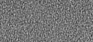
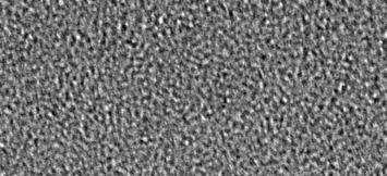
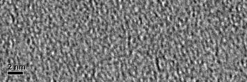
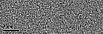
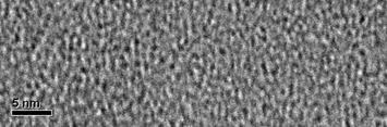
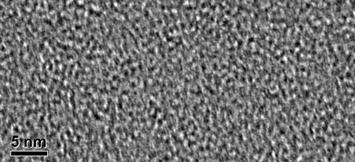
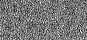
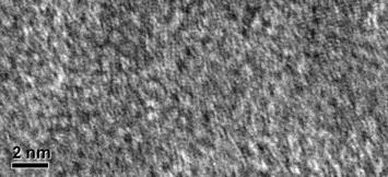
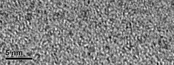
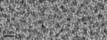
18 SiN:metal A System: 10 nm TEM Films Insulating Switching Switching Switching 5 nm SiN SiN+ x1% metal SiN+x2% metal SiN+x3%metal SiN+x4% metal SiN+x5% metal SiN+x6% metal metal Switching Switching Conducting Metal-rich Nanoparticles (Percolating) Conducting


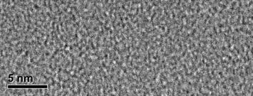
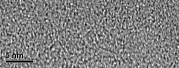
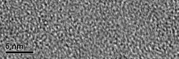
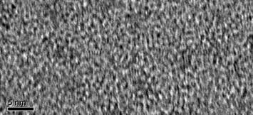
19 Oxide A:Pt System 5 nm Insulating Oxide Oxide+ x1% Pt Oxide+x2% Pt Oxide +x3% Pt Switching Switching Conducting (percolating) Metal-rich Nanoparticles Irrelevant for Nanometallic Switching
20 Metallic Nanoparticle? (SiO 2 :f Pt) Calibr rated Reflectio on (%) f Pt f ~ 0.2 Fused Silica f ~ 0.5 f ~ 0.37 f ~ 0.3 f ~ Wavelength (nm) Pt < 0.3: No Metallic Nanoparticle Plasmon Resonance: Signature of Metallic Nanoparticles
21 Capacitance (HR): SiN:Metal A f critical C = C diel + C met NP I C met NP ~ n met NP r 2 met NP r Switching % ~ n met NP r 3 met NP % Metal C met NP ~ %/r met NP f metal < f critical : No Metallic Nanoparticle
22 Reality Check Scaling: x nm times x nm Endurance: >10 7 cycles
23 Electronic Transition?
24 Fundamentally Different Features T Initial State Electrode s Work Functions, B UV R C Pulse Width,
25 Initial State No forming Initial state: metal High breakdown voltage >15 V
26 Top & Bottom Electrodes Must Be Different ø TE (ev) ø BE (ev) V s Polarity SiO 2 :Pt Pt 5.65 SRO Pt 5.65 Mo Mo 4.6 SRO I (ma) R ( ) Ag 4.26 Pt Pt 5.65 Ta V (V) + : Counter clockwise SiN 3/4 :Pt Pt 5.65 SRO LaAlO 3 : Pt 5.65 SRO LaNiO 3 Au 5.10 SRO Ag 4.26 SRO LaAlO 3 : Pt 5.65 SRO SrRuO 3 CaZrO 3 : Pt 5.65 SRO LaNiO 3 CaZrO 3 : Pt 5.65 SRO SrRuO 3 I (ma) V (V) -: Clockwise R ( )
27 UV Resets Memory: Electronic Pt, 5.6eV CaZrO 3 :LaNiO 3 SrTiO 3 SrRuO 3, 5.0eV Inten nsity UV light 4.2 ev 3.4 ev 3.0 ev Wavelength (nm) Res sistance ( ) UV off UV on LR UV off Time (sec) UV off UV on HR UV off Time (sec) Not an ionic effect
28 Electronic Transition: UV-triggered Pt SiO 2 :Pt Fused SiO 2 SrRuO 3 or Mo UV light 100k 100k R 10k UV on R ( 10k 1k UV on 1k Time (sec) Time (sec) Not an ionic effect
29 R HR Dependence Resis stance ( ) (100 m) 2 (60 m) 2 (40 m) 2 (20 m) 2 (10 m) Voltage (V) Resist tivity ( cm m) nm 20nm 17nm Area (cm 2 ) Obeys Ohm s law (R HRS 1/A) Extreme thickness dependence!
30 Non-Ohmic Thickness Dependence mm 2 ) A ( m R ~ exp(δ/ HR ) R x (nm) > (HR State) t Wave Function ~ exp(- / HR ) HR Violates Ohm s Law
31 ζ : Decreased by trapped charge mm 2 ) A ( m R ~ exp( / ) (nm) )20 10 R x (nm) Diffusion length ( ) : HR and LR f f ζ HR (nm) ζ LR (nm)
32 Symmetric Capacitance: Higher for HRS Equivalent Circuit 6000 Line & BE & Film / connecti interface Device on -Z im ( ) 3000 HRS@0V HRS@0.4V HRS@0.8V HRS@1.2V LRS Only at very high Z real ( ) No Interface Barrier: Symmetric C(V)
33 No Pulse Width Effect (>RC time) No Rate Dependence: Not AMemristor! > RC: Same switching voltage regardless of < < RC: Increasing switching voltage at smaller Same observations for HR-LR and LR-HR switching RC Time = R Line Line C Cell Cell ~ Cell Area Prediction: Same switching voltage down to ps in sub- m devices
34 Device Performance Retention Variance
35 Memory Retention Resist tance ( ) C HRS: >10ms 100ns LRS: >10ms 100ns Resist tance ( ) t retention /t write HRS: >10ms 100ns LRS: >10ms 100ns 10yr time (sec) t retention /t write Good retention regardless of programming speed

 Read @ < 0.")
36 Retention per Constant Voltage Stressing Test (sec) LR to HR V + *= V 1.6V V 27V 2.7V V 5.5V V m+ (V) 2 ) ln( V m years 1.1V 1.6V V + *= 2.3V 2.7V 45V 4.5V 5.5V /V m+ (V -1 ) < 0.4 V >10 year data retention t Fowler-Nordheim Tunneling over Barrier d: 15nm~ nmthick 2.6
37 Retention per Constant Voltage Stressing Test HR to LR (sec c) V *= 1.25V V 2.6V 3.6V V m (V) < 0.4 V >10 year data retention
38 Switching Uniformity R distribution rrent (A) Cu k cycles Applied voltage (V).1V ( ) 10k 1k ±4V, 100ns # of switching F(x) Cumulative probability, LRS HRS Resistance, x ( ) Highly reproducible on-offoff Narrowly distributed resistance
39 Switching Uniformity: Weibull plot Weibull plot (R) F( x) 1 exp( ( x / x0) k ) Ln(-Ln(1-F(x) )) LRS HRS V off (LRS HRS) -V on (HRS LRS) Ln(x) () k /μ R HRS R LRS Higher Weibull exponent k: more uniformity (lower /μ)
40 Switching Uniformity: R HRS & V switching Weibull distribution (analytic relation) / [ (1 2 2 / k) (1 1/ (1 1/ k) k)] 1/ 2 k Our Device R HRS / TiO 2 (DC) [1] TiO 2 :Pt (DC) [1] HfO 2 (AC) [2] HfO 2 :Al (AC) [2] NiO (DC) [3] NiO (AC) [3] NiO:Ti (DC) [4] NiO:Ti (AC) [4] Cu x O (AC) [5] ZnO:Mn (DC) [6] TaO (AC) [7] x PCMO (DC) [8] our device Weibull plot k 100 TiO 10 2 [1] TiO 2 :Pt [1] HfO 2 [2] HfO 1 2 :Al [2] NiO [3] NiO:Ti [4] ZnO:Mn [6] our device (V off ) 0.1 our device (-V on ) Weibull plot V switching / 1.K. Tsunoda et al., Tech. Dig. International Electron Devices Meeting 2007, B. Gao et al., Tech. Dig. Symposium on VLSI Technology 2009, M.-J. Lee et al.,, Tech. Dig. International Electron Devices Meeting 2007, A. Chen et al., Tech. Dig. International Electron Devices Meeting 2005, Y. C. Yang et al., Nano Lett. 2009, 9, W.-Y. Chang et al., Appl. Phys. Lett. 2009, 95, Z. Wei et al., Tech. Dig. International Electron Devices Meeting 2008, D. -J. Seong et al., Tech. Dig. International Electron Devices Meeting 2009,
41 Intermediate States: Metals or Insulators?
42 Intermediate States Insulator or Metal? Cur rrent (ma) 15 L Voltage (V) Resis stance ( ) L L Temperature (K) Resis stance ( ) L Temperature (K) FIT: Fluctuation-induced Tunneling Elastic tunneling 0 0 l 2 =area R/2 R/2 G ( T) G exp GV ( ) G 0, T C n T w G (1/ ) 10-2 (1/ ) Experimental FIT fitting Experimental Fitting T T K 250K exp( V / V0 ) 1 h exp( V / V ) 1 V 0 G Voltage (V) T(K) FIT
43 Intermediate States Insulator or Metal? Cur rrent (ma) Resis stance ( ) 10 9 L2 15 L L1 Voltage (V) Temperature (K) Resist tance ( ) 10 9 L2 Temperature (K) Reduced Activation Energy 10 1 L2 0 Insulator W T dln ( T) dt W 10 0 Metal Temperature (K) Multi-step on-switching: insulator-bad metal-metal transition Multi-state Multi-filament
44 Nanometallic RRAM Size-dependent d Nanometallicity it Metal Insulator Transition Random Materials Purely Electronic Switching
45 Conclusions Nanometallicty t : a size effect unique to random materials MIT: : triggered via δ, f, V, & photon; switching due to changing localization length, direction controlled by electrode work function Thank You Device properties: highly reproducible switching parameters, short read/write time independent of voltage, long retention time, adjustable switching parameters Nanostructure: metallic nanoparticles irrelevant
Electrical and Reliability Characteristics of RRAM for Cross-point Memory Applications. Hyunsang Hwang
 Electrical and Reliability Characteristics of RRAM for Cross-point Memory Applications Hyunsang Hwang Dept. of Materials Science and Engineering Gwangju Institute of Science and Technology (GIST), KOREA
Influence of electrode materials on CeO x based resistive switching
 Influence of electrode materials on CeO x based resistive switching S. Kano a, C. Dou a, M. Hadi a, K. Kakushima b, P. Ahmet a, A. Nishiyama b, N. Sugii b, K. Tsutsui b, Y. Kataoka b, K. Natori a, E. Miranda
Flexible nonvolatile polymer memory array on
 Supporting Information for Flexible nonvolatile polymer memory array on plastic substrate via initiated chemical vapor deposition Byung Chul Jang, #a Hyejeong Seong, #b Sung Kyu Kim, c Jong Yun Kim, a
Resistive Memories Based on Amorphous Films
 Resistive Memories Based on Amorphous Films Wei Lu University of Michigan Electrical Engineering and Computer Science Crossbar Inc 1 Introduction Hysteretic resistive switches and crossbar structures Simple
Mechanism of Switching and Related Challenges in Transition Metal Oxide Based RRAM Devices
 Mechanism of Switching and Related Challenges in Transition Metal Oxide Based RRAM Devices Rashmi Jha and Branden Long Dept. of Electrical Engineering and Computer Science University of Toledo Toledo,
Low Power Phase Change Memory via Block Copolymer Self-assembly Technology
 Low Power Phase Change Memory via Block Copolymer Self-assembly Technology Beom Ho Mun 1, Woon Ik Park 1, You Yin 2, Byoung Kuk You 1, Jae Jin Yun 1, Kung Ho Kim 1, Yeon Sik Jung 1*, and Keon Jae Lee 1*
NRAM: High Performance, Highly Reliable Emerging Memory
 NRAM: High Performance, Highly Reliable Emerging Memory Sheyang Ning,2, Tomoko Ogura Iwasaki, Darlene Viviani 2, Henry Huang 2, Monte Manning 2, Thomas Rueckes 2, Ken Takeuchi Chuo University 2 Nantero
Novel Devices and Circuits for Computing
 Novel Devices and Circuits for Computing UCSB 594BB Winter 2013 Lecture 3: ECM cell Class Outline ECM General features Forming and SET process RESET Variants and scaling prospects Equivalent model Electrochemical
Supplementary Materials for
 Supplementary Materials for Extremely Low Operating Current Resistive Memory Based on Exfoliated 2D Perovskite Single Crystals for Neuromorphic Computing He Tian,, Lianfeng Zhao,, Xuefeng Wang, Yao-Wen
Fabrication and Measurement of Spin Devices. Purdue Birck Presentation
 Fabrication and Measurement of Spin Devices Zhihong Chen School of Electrical and Computer Engineering Birck Nanotechnology Center, Discovery Park Purdue University Purdue Birck Presentation zhchen@purdue.edu
Bipolar resistive switching in amorphous titanium oxide thin films
 Bipolar resistive switching in amorphous titanium oxide thin films Hu Young Jeong and Jeong Yong Lee Department of Materials Science and Engineering, KAIST, Daejeon 305-701, Korea Min-Ki Ryu and Sung-Yool
An interfacial investigation of high-dielectric constant material hafnium oxide on Si substrate B
 Thin Solid Films 488 (2005) 167 172 www.elsevier.com/locate/tsf An interfacial investigation of high-dielectric constant material hafnium oxide on Si substrate B S.C. Chen a, T, J.C. Lou a, C.H. Chien
Scaling behaviors of RESET voltages and currents in unipolar
 Scaling behaviors of RESET voltages and currents in unipolar resistance switching S. B. Lee, 1 S. C. Chae, 1 S. H. Chang, 1 J. S. Lee, 2 S. Seo, 3 B. Kahng, 2 and T. W. Noh 1,a) 1 ReCOE & FPRD, Department
Supporting Information
 Supporting Information Monolithically Integrated Flexible Black Phosphorus Complementary Inverter Circuits Yuanda Liu, and Kah-Wee Ang* Department of Electrical and Computer Engineering National University
Analysis of charge-transport properties in GST materials for next generation phase-change memory devices. Fabio Giovanardi Tutor: Prof.
 Analysis of charge-transport properties in GST materials for next generation phase-change memory devices Fabio Giovanardi Tutor: Prof. Massimo Rudan The use of phase-change chalcogenide alloy films to
Introduction to Molecular Electronics. Lecture 1: Basic concepts
 Introduction to Molecular Electronics Lecture 1: Basic concepts Conductive organic molecules Plastic can indeed, under certain circumstances, be made to behave very like a metal - a discovery for which
Novel Devices and Circuits for Computing
 Novel Devices and Circuits for Computing UCSB 594BB Winter 213 Lectures 5 and 6: VCM cell Class Outline VCM = Valence Change Memory General features Forming SET and RESET Heating Switching models Scaling
Supporting Information
 Copyright WILEY-VCH Verlag GmbH & Co. KGaA, 69469 Weinheim, Germany, 2017. Supporting Information for Adv. Mater., DOI: 10.1002/adma.201602976 Direct Observations of Nanofilament Evolution in Switching
Planar Organic Photovoltaic Device. Saiful I. Khondaker
 Planar Organic Photovoltaic Device Saiful I. Khondaker Nanoscience Technology Center and Department of Physics University of Central Florida http://www.physics.ucf.edu/~khondaker W Metal 1 L ch Metal 2
J. Price, 1,2 Y. Q. An, 1 M. C. Downer 1 1 The university of Texas at Austin, Department of Physics, Austin, TX
 Understanding process-dependent oxygen vacancies in thin HfO 2 /SiO 2 stacked-films on Si (100) via competing electron-hole injection dynamic contributions to second harmonic generation. J. Price, 1,2
Experimental and Theoretical Study of Electrode Effects in HfO2 based RRAM
 Experimental and Theoretical Study of Electrode Effects in HfO2 based RRAM C. Cagli 1, J. Buckley 1, V. Jousseaume 1, T. Cabout 1, A. Salaun 1, H. Grampeix 1, J. F. Nodin 1,H. Feldis 1, A. Persico 1, J.
L ECE 4211 UConn F. Jain Scaling Laws for NanoFETs Chapter 10 Logic Gate Scaling
 L13 04202017 ECE 4211 UConn F. Jain Scaling Laws for NanoFETs Chapter 10 Logic Gate Scaling Scaling laws: Generalized scaling (GS) p. 610 Design steps p.613 Nanotransistor issues (page 626) Degradation
Stabilizing the forming process in unipolar resistance switching
 Stabilizing the forming process in unipolar resistance switching using an improved compliance current limiter S. B. Lee, 1 S. H. Chang, 1 H. K. Yoo, 1 and B. S. Kang 2,a) 1 ReCFI, Department of Physics
Thermal Oxidation of Si
 Thermal Oxidation of General Properties of O 2 Applications of thermal O 2 Deal-Grove Model of Oxidation Thermal O 2 is amorphous. Weight Density = 2.20 gm/cm 3 Molecular Density = 2.3E22 molecules/cm
Neuromorphic computing with Memristive devices. NCM group
 Neuromorphic computing with Memristive devices NCM group Why neuromorphic? New needs for computing Recognition, Mining, Synthesis (Intel) Increase of Fault (nanoscale engineering) SEMICONDUCTOR TECHNOLOGY
Supplementary Figures
 Supplementary Figures Supplementary Figure 1 Thickness calibration of PVDF layers using atomic force microscopy. (a-d) Tapping AFM images of 1 L, 2 Ls, 4 Ls and 20 Ls PVDF films, respectively on Au-coated
cermets), the bulk percolation limit (when the slope is zero) ranges from 0.40 to 0.65 for
, the bulk percolation limit (when the slope is zero) ranges from 0.40 to 0.65 for") SUPPLEMENTARY INFORMATION A size-dependent nanoscale metal-insulator transition in random materials Supplementary Information Albert B. K. Chen *, Soo Gil Kim *, Yudi Wang *, Wei-Shao Tung & I-Wei Chen
SUPPLEMENTARY INFORMATION A size-dependent nanoscale metal-insulator transition in random materials Supplementary Information Albert B. K. Chen *, Soo Gil Kim *, Yudi Wang *, Wei-Shao Tung & I-Wei Chen
Gold Nanoparticles Floating Gate MISFET for Non-Volatile Memory Applications
 Gold Nanoparticles Floating Gate MISFET for Non-Volatile Memory Applications D. Tsoukalas, S. Kolliopoulou, P. Dimitrakis, P. Normand Institute of Microelectronics, NCSR Demokritos, Athens, Greece S. Paul,
MIT Amorphous Materials
 MIT 3.071 Amorphous Materials 10: Electrical and Transport Properties Juejun (JJ) Hu 1 After-class reading list Fundamentals of Inorganic Glasses Ch. 14, Ch. 16 Introduction to Glass Science and Technology
Song and Feng Pan b) * Laboratory of Advanced Materials (MOE), School of Materials Science and Engineering,
 * Laboratory of Advanced Materials (MOE), School of Materials Science and Engineering,") Electronic Supplementary Material (ESI) for Nanoscale. This journal is The Royal Society of Chemistry 2015 Supplementary Information to Forming-free and self-rectifying resistive switching of the simple
Electronic Supplementary Material (ESI) for Nanoscale. This journal is The Royal Society of Chemistry 2015 Supplementary Information to Forming-free and self-rectifying resistive switching of the simple
1 Ionic Memory Technology
 j1 1 Ionic Memory Technology An Chen Ionic memory devices based on ion migration and electrochemical reactions have shown promising characteristics for next-generation memory technology. Both cations (e.g.,
MSE 310/ECE 340: Electrical Properties of Materials Fall 2014 Department of Materials Science and Engineering Boise State University
 MSE 310/ECE 340: Electrical Properties of Materials Fall 2014 Department of Materials Science and Engineering Boise State University Practice Final Exam 1 Read the questions carefully Label all figures
Carbon Nanotube Thin-Films & Nanoparticle Assembly
 Nanodevices using Nanomaterials : Carbon Nanotube Thin-Films & Nanoparticle Assembly Seung-Beck Lee Division of Electronics and Computer Engineering & Department of Nanotechnology, Hanyang University,
RRAM technology: From material physics to devices. Fabien ALIBART IEMN-CNRS, Lille
 RRAM technology: From material physics to devices Fabien ALIBART IEMN-CNRS, Lille Outline Introduction: RRAM technology and applications Few examples: Ferroelectric tunnel junction memory Mott Insulator
Moores Law for DRAM. 2x increase in capacity every 18 months 2006: 4GB
 MEMORY Moores Law for DRAM 2x increase in capacity every 18 months 2006: 4GB Corollary to Moores Law Cost / chip ~ constant (packaging) Cost / bit = 2X reduction / 18 months Current (2008) ~ 1 micro-cent
Large Storage Window in a-sinx/nc-si/a-sinx Sandwiched Structure
 2017 Asia-Pacific Engineering and Technology Conference (APETC 2017) ISBN: 978-1-60595-443-1 Large Storage Window in a-sinx/nc-si/a-sinx Sandwiched Structure Xiang Wang and Chao Song ABSTRACT The a-sin
Thermal Resistance (measurements & simulations) In Electronic Devices
 In Electronic Devices") Thermal Resistance (measurements & simulations) In Electronic Devices A short online course PART 3 Eric Pop Electrical Engineering, Stanford University 1 Topics 1) Basics of Joule Heating 2) Heating in
Thermal Resistance (measurements & simulations) In Electronic Devices A short online course PART 3 Eric Pop Electrical Engineering, Stanford University 1 Topics 1) Basics of Joule Heating 2) Heating in
Supplementary Figure S1. AFM images of GraNRs grown with standard growth process. Each of these pictures show GraNRs prepared independently,
 Supplementary Figure S1. AFM images of GraNRs grown with standard growth process. Each of these pictures show GraNRs prepared independently, suggesting that the results is reproducible. Supplementary Figure
Strong-electric-field effects and antenna resonances in single-wall carbon nanotube films
 Strong-electric-field effects and antenna resonances in single-wall carbon nanotube films Dalius Seliuta Center for Physical Sciences and Technology, Vilnius, Lithuania Liudas Subačius, Irmantas Kašalynas,
Optimization of the Dielectric Constant of a Blocking Dielectric in the Nonvolatile Memory Based on Silicon Nitride
 ISSN 8756-699, Optoelectronics, Instrumentation and Data Processing, 9, Vol. 45, No. 4, pp. 48 5. c Allerton Press, Inc., 9. Original Russian Text c Y. N. Novikov, V. A. Gritsenko, K. A. Nasyrov, 9, published
Quantum Mechanical Simulation for Ultra-thin High-k Gate Dielectrics Metal Oxide Semiconductor Field Effect Transistors
 Mechanical Simulation for Ultra-thin High-k Gate Dielectrics Metal Oxide Semiconductor Field Effect Transistors Shih-Ching Lo 1, Yiming Li 2,3, and Jyun-Hwei Tsai 1 1 National Center for High-Performance
CONDUCTIVITY MECHANISMS AND BREAKDOWN CHARACTERISTICS OF NIOBIUM OXIDE CAPACITORS
 CONDUCTIVITY MECHANISMS AND BREAKDOWN CHARACTERISTICS OF NIOBIUM OXIDE CAPACITORS J. Sikula, J. Hlavka, V. Sedlakova and L. Grmela Czech Noise Research Laboratory, Brno University of Technology Technicka,
Fabrication and Characteristic Investigation of Multifunctional Oxide p-n Heterojunctions
 Advances in Science and Technology Vol. 45 (2006) pp. 2582-2587 online at http://www.scientific.net (2006) Trans Tech Publications, Switzerland Fabrication and Characteristic Investigation of Multifunctional
2 Title: "Ultrathin flexible electronic device based on tunneling effect: a flexible ferroelectric tunnel
 Electronic Supplementary Material (ESI) for Journal of Materials Chemistry C. This journal is The Royal Society of Chemistry 208 Supplementary information 2 Title: "Ultrathin flexible electronic device
Computational Materials Design and Discovery Energy and Electronic Applications Synthesis Structure Properties
 Computational Materials Design and Discovery Energy and Electronic Applications Synthesis Structure Properties Supercapacitors Rechargeable batteries Supercomputer Photocatalysts Fuel cell catalysts First
Electrical Properties of Ti/Au/SiO,/InP Structures
 M. PATEL and N. M. RAVNDRA: Electrical Properties of Ti/Au/SiO,/nP 567 phys. stat. sol. (a) 134, 567 (1992) Subject classification: 73.40; 85; S7.11 Microelectronics Research Center, New Jersey nstitute
RC Studies Relaxation Oscillator
 RC Studies Relaxation Oscillator Introduction A glass tube containing neon gas will give off its characteristic light when the voltage across the tube exceeds a certain value. The value corresponds to
AN ABSTRACT OF THE THESIS OF
 AN ABSTRACT OF THE THESIS OF Santosh Murali for the degree of Master of Science in Electrical and Computer Engineering presented on December 20, 2011. Title: Investigation of Bipolar Resistive Switching
Frequency dispersion effect and parameters. extraction method for novel HfO 2 as gate dielectric
 048 SCIENCE CHINA Information Sciences April 2010 Vol. 53 No. 4: 878 884 doi: 10.1007/s11432-010-0079-8 Frequency dispersion effect and parameters extraction method for novel HfO 2 as gate dielectric LIU
Computational Science Studies toward Future Nano-Devices. Kenji Shiraishi. University of Tsukuba
 Computational Science Studies toward Future Nano-Devices Kenji Shiraishi University of Tsukuba 1 1. Introduction Contents 2. Key physics in ionic materials obtained by computational sciences. 3. Operation
Tunneling transport. Courtesy Prof. S. Sawyer, RPI Also Davies Ch. 5
 unneling transport Courtesy Prof. S. Sawyer, RPI Also Davies Ch. 5 Electron transport properties l e : electronic mean free path l φ : phase coherence length λ F : Fermi wavelength ecture Outline Important
(Co-PIs-Mark Brongersma, Yi Cui, Shanhui Fan) Stanford University. GCEP Research Symposium 2013 Stanford, CA October 9, 2013
 Stanford University. GCEP Research Symposium 2013 Stanford, CA October 9, 2013") High-efficiency thin film nano-structured multi-junction solar James S. cells Harris (PI) (Co-PIs-Mark Brongersma, Yi Cui, Shanhui Fan) Stanford University GCEP Research Symposium 2013 Stanford, CA October
High-efficiency thin film nano-structured multi-junction solar James S. cells Harris (PI) (Co-PIs-Mark Brongersma, Yi Cui, Shanhui Fan) Stanford University GCEP Research Symposium 2013 Stanford, CA October
ECE 340 Lecture 39 : MOS Capacitor II
 ECE 340 Lecture 39 : MOS Capacitor II Class Outline: Effects of Real Surfaces Threshold Voltage MOS Capacitance-Voltage Analysis Things you should know when you leave Key Questions What are the effects
Enhancing the Performance of Organic Thin-Film Transistor using a Buffer Layer
 Proceedings of the 9th International Conference on Properties and Applications of Dielectric Materials July 19-23, 29, Harbin, China L-7 Enhancing the Performance of Organic Thin-Film Transistor using
Metallic: 2n 1. +n 2. =3q Armchair structure always metallic = 2
 Properties of CNT d = 2.46 n 2 2 1 + n1n2 + n2 2π Metallic: 2n 1 +n 2 =3q Armchair structure always metallic a) Graphite Valence(π) and Conduction(π*) states touch at six points(fermi points) Carbon Nanotube:
1. Depleted heterojunction solar cells. 2. Deposition of semiconductor layers with solution process. June 7, Yonghui Lee
 1. Depleted heterojunction solar cells 2. Deposition of semiconductor layers with solution process June 7, 2016 Yonghui Lee Outline 1. Solar cells - P-N junction solar cell - Schottky barrier solar cell
Supplementary Information. All Nanocellulose Nonvolatile Resistive Memory
 Supplementary Information All Nanocellulose Nonvolatile Resistive Memory Umberto Celano, Kazuki Nagashima, Hirotaka Koga, Masaya Nogi, Fuwei Zhuge, Gang Meng, Yong He, Jo De Boeck, Malgorzata Jurczak,
Solar cells operation
 Solar cells operation photovoltaic effect light and dark V characteristics effect of intensity effect of temperature efficiency efficency losses reflection recombination carrier collection and quantum
Electrical measurements of voltage stressed Al 2 O 3 /GaAs MOSFET
 Microelectronics Reliability xxx (2007) xxx xxx www.elsevier.com/locate/microrel Electrical measurements of voltage stressed Al 2 O 3 /GaAs MOSFET Z. Tang a, P.D. Ye b, D. Lee a, C.R. Wie a, * a Department
Photovoltage phenomena in nanoscaled materials. Thomas Dittrich Hahn-Meitner-Institute Berlin
 Photovoltage phenomena in nanoscaled materials Thomas Dittrich Hahn-Meitner-Institute Berlin 1 2 Introduction From bulk to nanostructure: SPV on porous Si Retarded SPV response and its origin Photovoltage
The goal of this project is to enhance the power density and lowtemperature efficiency of solid oxide fuel cells (SOFC) manufactured by atomic layer
 manufactured by atomic layer") Stanford University Michael Shandalov1, Shriram Ramanathan2, Changhyun Ko2 and Paul McIntyre1 1Department of Materials Science and Engineering, Stanford University 2Division of Engineering and Applied
Stanford University Michael Shandalov1, Shriram Ramanathan2, Changhyun Ko2 and Paul McIntyre1 1Department of Materials Science and Engineering, Stanford University 2Division of Engineering and Applied
Analysis of Band-to-band. Tunneling Structures. Title of Talk. Dimitri Antoniadis and Judy Hoyt (PIs) Jamie Teherani and Tao Yu (Students) 8/21/2012
 Jamie Teherani and Tao Yu (Students) 8/21/2012") 1 Analysis of Band-to-band Title of Talk Tunneling Structures Dimitri Antoniadis and Judy Hoyt (PIs) Jamie Teherani and Tao Yu (Students) 8/21/2012 A Science & Technology Center Vertical Type-II TFET Structure
1 Analysis of Band-to-band Title of Talk Tunneling Structures Dimitri Antoniadis and Judy Hoyt (PIs) Jamie Teherani and Tao Yu (Students) 8/21/2012 A Science & Technology Center Vertical Type-II TFET Structure
DISTRIBUTION OF POTENTIAL BARRIER HEIGHT LOCAL VALUES AT Al-SiO 2 AND Si-SiO 2 INTERFACES OF THE METAL-OXIDE-SEMICONDUCTOR (MOS) STRUCTURES
 STRUCTURES") DISTRIBUTION OF POTENTIAL BARRIER HEIGHT LOCAL VALUES AT Al-SiO 2 AND Si-SiO 2 INTERFACES OF THE ETAL-OXIDE-SEICONDUCTOR (OS) STRUCTURES KRZYSZTOF PISKORSKI (kpisk@ite.waw.pl), HENRYK. PRZEWLOCKI Institute
DISTRIBUTION OF POTENTIAL BARRIER HEIGHT LOCAL VALUES AT Al-SiO 2 AND Si-SiO 2 INTERFACES OF THE ETAL-OXIDE-SEICONDUCTOR (OS) STRUCTURES KRZYSZTOF PISKORSKI (kpisk@ite.waw.pl), HENRYK. PRZEWLOCKI Institute
Experimental and theoretical understanding of Forming, SET and RESET operations in Conductive Bridge RAM (CBRAM) for memory stack optimization
 for memory stack optimization") Experimental and theoretical understanding of Forming, SET and RESET operations in Conductive Bridge RAM (CBRAM) for memory stack optimization J. Guy, G. Molas, P. Blaise, C. Carabasse, M. Bernard, A.
Experimental and theoretical understanding of Forming, SET and RESET operations in Conductive Bridge RAM (CBRAM) for memory stack optimization J. Guy, G. Molas, P. Blaise, C. Carabasse, M. Bernard, A.
Symetrix Corporation Background
 Symetrix Corporation Background Symetrix has strong history as IP provider > 25 years of development >200 U.S. and foreign patents. > $70M in research revenues, royalties and other income from development.
1. HP's memristor and applications 2. Models of resistance switching. 4. 3D circuit architectures 5. Proposal for evaluation framework
 OUTL LINE 1. HP's memristor and applications 2. Models of resistance switching 3. Volatility speed tradeo ffs 4. 3D circuit architectures 5. Proposal for evaluation framework HP S MEMRISTOR memristor =
23.0 Review Introduction
 EE650R: Reliability Physics of Nanoelectronic Devices Lecture 23: TDDB: Measurement of bulk trap density Date: Nov 13 2006 Classnotes: Dhanoop Varghese Review: Nauman Z Butt 23.0 Review In the last few
SUPPLEMENTARY INFORMATION
 doi:10.1038/nature17653 Supplementary Methods Electronic transport mechanism in H-SNO In pristine RNO, pronounced electron-phonon interaction results in polaron formation that dominates the electronic
CONSTANT CURRENT STRESS OF ULTRATHIN GATE DIELECTRICS
 CONSTANT CURRENT STRESS OF ULTRATHIN GATE DIELECTRICS Y. Sun School of Electrical & Electronic Engineering Nayang Technological University Nanyang Avenue, Singapore 639798 e-mail: 14794258@ntu.edu.sg Keywords:
Thermoelectric Oxide Materials For Electric Power Generation
 Thermoelectric Oxide Materials For Electric Power Generation Kunihito Koumoto Nagoya University, Graduate School of Engineering CREST, Japan Science and Technology Agency 1. Thermoelectric Energy Conversion
Lecture 6: 2D FET Electrostatics
 Lecture 6: 2D FET Electrostatics 2016-02-01 Lecture 6, High Speed Devices 2014 1 Lecture 6: III-V FET DC I - MESFETs Reading Guide: Liu: 323-337 (he mainly focuses on the single heterostructure FET) Jena:
Chapter 6 ELECTRICAL CONDUCTIVITY ANALYSIS
 Chapter 6 ELECTRICAL CONDUCTIVITY ANALYSIS CHAPTER-6 6.1 Introduction The suitability and potentiality of a material for device applications can be determined from the frequency and temperature response
Redefining the Speed Limit of Phase Change Memory Revealed by Time-resolved Steep Threshold-Switching Dynamics of AgInSbTe Devices
 Supplementary Information Redefining the Speed Limit of Phase Change Memory Revealed by ime-resolved Steep hreshold-switching Dynamics of AgInSbe Devices Krishna Dayal Shukla 1, Nishant Saxena 1, Suresh
Gate Carrier Injection and NC-Non- Volatile Memories
 Gate Carrier Injection and NC-Non- Volatile Memories Jean-Pierre Leburton Department of Electrical and Computer Engineering and Beckman Institute University of Illinois at Urbana-Champaign Urbana, IL 61801,
Electronic Supplementary Information
 Electronic Supplementary Material (ESI) for Journal of Materials Chemistry C. This journal is The Royal Society of Chemistry 2017 Electronic Supplementary Information Trifunctional NiO Ag NiO Electrodes
Nanostrukturphysik (Nanostructure Physics)
") Nanostrukturphysik (Nanostructure Physics) Prof. Yong Lei & Dr. Yang Xu Fachgebiet 3D-Nanostrukturierung, Institut für Physik Contact: yong.lei@tu-ilmenau.de; yang.xu@tu-ilmenau.de Office: Unterpoerlitzer
Nanostrukturphysik (Nanostructure Physics) Prof. Yong Lei & Dr. Yang Xu Fachgebiet 3D-Nanostrukturierung, Institut für Physik Contact: yong.lei@tu-ilmenau.de; yang.xu@tu-ilmenau.de Office: Unterpoerlitzer
Resistive Random Access Memories (RRAMs)
") Resistive Random Access Memories (RRAMs) J. Joshua Yang HP Labs, Palo Alto, CA, USA (currently) ECE Dept., Umass Amherst (Jan/2015 - ) 1 Copyright 2010 Hewlett-Packard Development Company, L.P. Resistive
Resistive Random Access Memories (RRAMs) J. Joshua Yang HP Labs, Palo Alto, CA, USA (currently) ECE Dept., Umass Amherst (Jan/2015 - ) 1 Copyright 2010 Hewlett-Packard Development Company, L.P. Resistive
Ferroelectrics. Spartak Gevorgian. Department of Microtechnology and Nanoscience Chalmers University of Technology Gothenburg, Sweden
 Ferroelectrics Material Properties, Processing, and Microwave Applications Spartak Gevorgian Department of Microtechnology and Nanoscience Chalmers University of Technology Gothenburg, Sweden Norwegian
H-treatment impact on conductivefilament. formation and stability in
 H-treatment impact on conductivefilament formation and stability in Ta 2 O 5 -based resistive-switching memory cells L. Goux 1,*, J. Y. Kim 2, B. Magyari-Kope 2, Y. Nishi 2, A. Redolfi 1, M. Jurczak 1
MOS Transistor Properties Review
 MOS Transistor Properties Review 1 VLSI Chip Manufacturing Process Photolithography: transfer of mask patterns to the chip Diffusion or ion implantation: selective doping of Si substrate Oxidation: SiO
A Low-Noise Solid-State Nanopore Platform Based on a Highly Insulating Substrate
 SUPPORTING INFORMATION A Low-Noise Solid-State Nanopore Platform Based on a Highly Insulating Substrate Min-Hyun Lee, Ashvani Kumar, Kyeong-Beom Park, Seong-Yong Cho, Hyun-Mi Kim, Min-Cheol Lim, Young-Rok
Diamond-like carbon film deposition on PZT ferroelectrics and YBCO superconducting films using KrF excimer laser deposition
 Composites: Part B 30 (1999) 685 689 www.elsevier.com/locate/compositesb Diamond-like carbon film deposition on PZT ferroelectrics and YBCO superconducting films using KrF excimer laser deposition K. Ebihara*,
Semester Length Glass Courses and Glass Schools
 Lehigh University Lehigh Preserve US-Japan Winter School Semester Length Glass Courses and Glass Schools Winter 1-1-2008 Special lecture, Part 1: Nature-guided nanotechnology for chemical tectonics of
High Performance, Low Operating Voltage n-type Organic Field Effect Transistor Based on Inorganic-Organic Bilayer Dielectric System
 Journal of Physics: Conference Series PAPER OPEN ACCESS High Performance, Low Operating Voltage n-type Organic Field Effect Transistor Based on Inorganic-Organic Bilayer Dielectric System To cite this
Experimental and theoretical study of ultra-thin oxides
 Semicond. Sci. Technol. 13 (1998) A155 A159. Printed in the UK PII: S0268-1242(98)91837-5 Experimental and theoretical study of ultra-thin oxides E S Daniel, D Z-Y Ting and T C McGill T J Watson Sr Laboratory
Flexible Asymmetrical Solid-state Supercapacitors Based on Laboratory Filter Paper
 SUPPORTING INFORMATION Flexible Asymmetrical Solid-state Supercapacitors Based on Laboratory Filter Paper Leicong Zhang,,,# Pengli Zhu,,,#, * Fengrui Zhou, Wenjin Zeng, Haibo Su, Gang Li, Jihua Gao, Rong
VI. EIS STUDIES LEAD NANOPOWDER
 VI. EIS STUDIES LEAD NANOPOWDER 74 26. EIS Studies of Pb nanospheres Impedance (valid for both DC and AC), a complex resistance occurs when current flows through a circuit (composed of various resistors,
SPICE Modeling of STT-RAM for Resilient Design. Zihan Xu, Ketul Sutaria, Chengen Yang, Chaitali Chakrabarti, Yu (Kevin) Cao School of ECEE, ASU
 Cao School of ECEE, ASU") SPICE odeling of STT-RA for Resilient Design Zihan Xu, Ketul Sutaria, Chengen Yang, Chaitali Chakrabarti, Yu (Kevin) Cao School of ECEE, ASU OUTLINE - 2 - Heterogeneous emory Design A Promising Candidate:
SPICE odeling of STT-RA for Resilient Design Zihan Xu, Ketul Sutaria, Chengen Yang, Chaitali Chakrabarti, Yu (Kevin) Cao School of ECEE, ASU OUTLINE - 2 - Heterogeneous emory Design A Promising Candidate:
Large-Scale and Precise Nanoparticle Placement via Electrostatic Funneling
 Large-Scale and Precise Nanoparticle Placement via Electrostatic Funneling August 21, 2007 Seong Jin Koh Materials Science and Engineering The University of Texas at Arlington Acknowledgement Vishva Ray
Introduction to Thermoelectric Materials and Devices
 Introduction to Thermoelectric Materials and Devices 4th Semester of 2012 2012.03.29, Thursday Department of Energy Science Sungkyunkwan University Radioisotope Thermoelectric Generator (PbTe) Space probe
Reliability of semiconductor I Cs. Reliability of semiconductor I Cs plus
 M.I.T. Reliability of semiconductor I Cs plus spin-based electronics Read Campbell, p. 425-428 and Ch. 20. Sec. 20.1, 20.2; Plummer, Sec. 11.5.6 IC reliability: Yield =(#operating parts) / (total # produced)
Starting solution. Hydrolysis reaction under thermostatic conditions. Check of viscosity and deposition test SOL. Deposition by spin coating
 Supplementary Figures Tetramethyl orthosilicate (TMOS) Tetrahydrofuran anhydrous (THF) Trimethyl methoxy silane (TMMS) Trimethyl silil acetate (TMSA) Starting solution Hydrolysis reaction under thermostatic
Scaling Issues in Planar FET: Dual Gate FET and FinFETs
 Scaling Issues in Planar FET: Dual Gate FET and FinFETs Lecture 12 Dr. Amr Bayoumi Fall 2014 Advanced Devices (EC760) Arab Academy for Science and Technology - Cairo 1 Outline Scaling Issues for Planar
Steady-state diffusion is diffusion in which the concentration of the diffusing atoms at
 Chapter 7 What is steady state diffusion? Steady-state diffusion is diffusion in which the concentration of the diffusing atoms at any point, x, and hence the concentration gradient at x, in the solid,
Ovshinsky Effect by Quantum Mechanics
 Ovshinsky Effect by Quantum Mechanics Thomas V. Prevenslik Abstract Ovshinsky initiated scientific research in the field of amorphous and disordered materials that continues to this day. The Ovshinsky
Three-Dimensional Silicon-Germanium Nanostructures for Light Emitters and On-Chip Optical. Interconnects
 Three-Dimensional Silicon-Germanium Nanostructures for Light Emitters and On-Chip Optical eptember 2011 Interconnects Leonid Tsybeskov Department of Electrical and Computer Engineering New Jersey Institute
N ano scale l S il ii lco i n B ased N o nvo lat l i atl ie l M em ory r Chungwoo Kim, Ph.D.
 cw_kim@samsung.com Acknowledgements Collaboration Funding Outline Introduction Current research status Nano fabrication Process Nanoscale patterning SiN thin film Si Nanoparticle Nano devices Nanoscale
single-electron electron tunneling (SET)
") single-electron electron tunneling (SET) classical dots (SET islands): level spacing is NOT important; only the charging energy (=classical effect, many electrons on the island) quantum dots: : level spacing
single-electron electron tunneling (SET) classical dots (SET islands): level spacing is NOT important; only the charging energy (=classical effect, many electrons on the island) quantum dots: : level spacing
an introduction to Semiconductor Devices
 an introduction to Semiconductor Devices Donald A. Neamen Chapter 6 Fundamentals of the Metal-Oxide-Semiconductor Field-Effect Transistor Introduction: Chapter 6 1. MOSFET Structure 2. MOS Capacitor -
Nanomaterials for Plasmonic Devices. Lih J. Chen
 Nanomaterials for Plasmonic Devices Lih J. Chen Department of Materials Science and Engineering, National Tsing Hua University, Hsinchu, Taiwan Papers on Plasmon: 75,000 (6/25/2018) Papers on Plasmonics: