Bipolar resistive switching in amorphous titanium oxide thin films
|
|
|
- Godfrey Watson
- 6 years ago
- Views:
Transcription
1 Bipolar resistive switching in amorphous titanium oxide thin films Hu Young Jeong and Jeong Yong Lee Department of Materials Science and Engineering, KAIST, Daejeon , Korea Min-Ki Ryu and Sung-Yool Choi a) Electronics and Telecommunications Research Institute (ETRI) 161 Gajeong-Dong, Yuseong-Gu, Daejeon, , Korea Using isothermal and temperature-dependent electrical measurements, we investigated the resistive switching mechanism of amorphous titanium oxide thin films deposited by a plasma-enhanced atomic layer deposition method between two aluminum electrodes. We found a bipolar resistive switching behavior in the high temperature region (> 140 K), and two activation energies of shallow traps, ev and ev in the ohmic current regime. We also proposed that the bipolar resistive switching of amorphous TiO 2 thin films is governed by the transition of conduction mode from a bulk-limited SCLC model (Off state) to an interface-limited Schottky emission (On state), generated by the ionic movement of oxygen vacancies. a) Electronic mail: sychoi@etri.re.kr 1
2 Recent observations of the reversible resistive switching effect in metal-oxidemetal structures (MOM) with binary oxides of TiO 2 and NiO 3,4 2 have been reported for 1,2 next generation nonvolatile memory applications. To explain the microscopic origin of the resistive switching, various models have been proposed such as filamentary conducting paths, 5 trap-controlled space-charge-limited current (SCLC), 6 and interface Schottky contact or traps. 7 Although the versatile switching phenomena of TiO 2 were already reported in 1968 by Argall, 8 the resistive switching mechanism has not been clearly understood yet. Recently, we reported the resistive switching characteristics of Al/amorphous TiO 2 film/al devices and the application for the resistive random access memory (RRAM). 9 In this letter, we analyze the bipolar resistive switching mechanism in Al/TiO 2 /Al devices, by using isothermal and temperature-dependent I-V measurements. Using a plasma-enhanced atomic layer deposition (PEALD) method, the amorphous TiO 2 thin films were deposited onto Al bottom electrode of 60nm thickness patterned on silicon dioxide substrates. The line-shaped Al bottom electrodes of 60 µm width was formed using metal shadow mask by thermal evaporation method on a SiO 2 /Si substrate. To grow ultrathin TiO 2 films, we used titanium isopropoxide (Ti(OCH(CH 3 ) 2 ) 4 ; TTIP) and O 2 plasma as Ti precursor and oxygen source, respectively. We deposited amorphous titanium oxide thin films with a thickness of ~13 nm (300cycle) and a growth rate of nm/cycle at 180 o C. The line-shaped top Al electrodes of 60 µm width were deposited perpendicularly to the bottom electrodes, so that the cross-bar type memory cell area of 60 µm 60 µm (3600 µm 2 ) was fabricated. The I-V characteristics of the device were measured using a Keithley 4200 Semiconductor Characterization System in a DC sweep mode. The temperature-dependent electrical properties of Al/TiO 2 /Al devices was measured from 83K to 323K. The cross-sectional transmission electron microscopy (TEM) images of Al/TiO 2 /Al samples were obtained using a 300 kv JEOL JEM 3010 with a
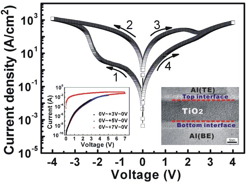
3 nm point resolution. Figure 1 shows a typical current density-voltage (J-V) curve of Al/TiO 2 /Al device performed at room temperature (298K). The voltage sweep sequence was indicated by the arrows. The pronounced hysteretic behavior was clearly observed, showing the resistance ratio of > 10 2 at a reading voltage (-1 V) without an initial forming process. Interestingly, when the positive bias was firstly applied to the device, the hysteresis did not occur, resulting in a failed state at 7V bias, as shown in the left inset of Fig. 1. Therefore, our device represents asymmetric bipolar resistance switching (BRS), 10 in which the negative bias changes the device from high-resistance state (HRS) to low-resistance state (LRS) and the positive bias from LRS to HRS. The asymmetric J-V characteristics of Al/TiO 2 /Al devices can be explained by the asymmetric interface formation, as reported by Yu et al. 9 The right inset of Fig. 1 shows a cross-sectional high resolution transmission electron microscopy (HRTEM) image of the fabricated layered film. The thickness of TiO 2 film was about ~14nm. The deposited TiO 2 films were amorphous phase as revealed by TEM image. Interestingly, it was also observed that the top and bottom amorphous interface layer were formed between Al metal electrodes, as indicated by bright contrast in the HRTEM image. In the case of the bottom interface, a native aluminum oxide with 2~3nm thickness was formed on the surface of Al bottom electrode. In contrast, the top interface layer was created by an out-diffusion of oxygen ions in TiO 2 layer, resulting in amorphous oxide layer. Thus, the inner domain of TiO 2 layer changed to TiO 2-x with oxygen deficiency which causes various defects such as oxygen vacancies (V x O, V + O, V ++ O ) or Ti +3 center. These defects can act as the charge trapping sites. In order to clarify the current conduction mechanism of Al/TiO 2 /Al device, we analyzed the J-V characteristics with respect to various conduction mechanisms: SCLC, Richardson-Schottky (R-S) thermionic emission, and Poole-Frenkel (P-F) conduction
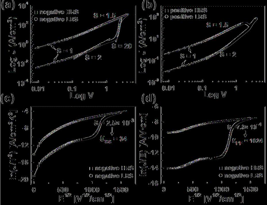
4 Figure 2(a) and (b) show the logarithmic plots of the J-V curve for the negative and positive voltage regions, respectively. In the first negative bias scan, shown in Fig. 2 (a), the slope of logj-logv plot (S) of the HRS changes from 1 to 2, 20, and 2 as V increases. This behavior is in qualitative agreement with the trap-associated SCLC theory. According to SCLC model, logj-logv plot exhibits linear ohmic conduction ( I V ), followed by a square dependence on voltage: I V 2, which corresponds to Child s law region. 13 When the applied voltage reaches to a certain threshold voltage V T (~ V) the current increases rapidly due to trap-filled condition. In a higher-voltage region V > V ), I V ( T is observed again. However, in the second negative sweep (LRS), the S values show just a single increase from 1 to 1.5. This is not simply explained by the SCLC model as generally observed in many oxide films. 6,10 Hence, it is reasonable to assume that the HRS and LRS follow two different conduction mechanisms. The linear fittings of the ln(j/t 2 ) vs E 1/2 and ln(j/e) vs E 1/2 is used to determine whether the Schottky emission or the Pool-Frenkel effect is the controlling conduction mechanism in high voltage region of negative HRS and >0.1V region of negative LRS, as shown in Fig. 2 (c) and (d) It can be seen that reasonable straight lines can be fitted in the high voltage region of LRS for both plots. The linear line slopes (S) of each plot are analyzed in Fig. 2 (c) and (d), from which we can calculate dynamic dielectric constants (ε r ) based on following equations, respectively 2 ε q 3 = SC 2 ( kts) 4πε 0 and ε PF = q 3 2 ( kts ) πε 0 Where S and S is the slope of the linear fitting obtained from the ln(j/t 2 ) vs E 1/2 and 4
5 ln(j/e) vs E 1/2, q is the electronic charge, kt is Boltzmann s constant times the absolute temperature, and ε 0 is the dielectric constant of free space. Because the extracted dielectric constant, ε SC ( ~ 34), is between low-frequency (static) dielectric constant and high-frequency (optical) dielectric constant ( ε = n 2, where n is the refractive index), Schottky emission is more likely to be the dominant conduction mechanism at the high electric field in the negative HRS and at > 0.1V region in the negative LRS. It is remarkable that our data is closer to the static dielectric value of TiO 2 (ε~ 40) 14 which is mainly contributed by ionic polarizability. Thus, it is believed that the change of current conduction mode of a Al/TiO 2 /Al stack is associated with the ionic movement like oxygen vacancies (ions). Although the transition from a bulk-limited conduction of SCLC to an electrode-limited conduction of Schottky typically occurs in high voltage regions, 12,15 the reversible change of two conduction modes, accompanying the resistance change, has not yet reported. To investigate the details of the defect (oxygen vacancy) characteristics in the amorphous titanium oxide films, temperature dependent I-V curves were measured in the temperature range from 83 to 323 K (Figure 3(a)). One notable finding is that the larger hysteresis was observed as temperature increases and a negligible switching behavior was shown in the low temperatures (T<140K). It is believed that temperature makes a critical effect in the resistive switching of amorphous thin films. This phenomenon can be understood with the assumption that the diffusivity of oxygen vacancies (ions) is also dependent on the temperature. In the low temperature, the movement of oxygen ions in the oxide lattice would not be easy. In order to deeply estimate the activation energies (E a ) of traps, the temperature dependence of the conductivity ( σ = σ 0 exp( E a / kt) ) at the ohmic current regions (- 0.1V ~ + 0.1V) was plotted in Fig. 3(b). The activation energies were 5
6 obtained from the slope of the least-squared fit lines. In the low temperature regions (T < 140 K), the value of E of both resistance states is the same as ev. However, in the high temperature (T > 140 K), the activation energies of both resistance states are separated. The energy level of high resistance state is ev and that of low resistance state is ev. These values are the activation energies of the shallow traps located near the conduction band edge. It is remarkable that the different resistance states also have unlike activation energies. However, it seems doubtful that low resistance state has a high activation energy. This is probably associated with the dissimilarity of the defect (oxygen vacancy) concentrations present on the inner bulk TiO 2-x layer in two different resistance states. Cronemeyer 16 reported that the electrical conductivity emerged from the ionization of either one or two trapped electrons from each oxygen vacancy and the decrease of thermal ionization appeared with an increase of oxygen vacancy concentration. The change of the activation energy of these shallow traps might be originated from that of the trap (oxygen vacancy) density in the bulk TiO 2-x caused by oxygen vacancy drift. On the basis of this result, we can explain that the low resistance state with traps of high activation energy could be exist due to low oxygen vacancy concentration. Based on above results, the schematic band diagrams of bipolar resistive switching in the amorphous titanium oxide thin films was illustrated in Fig. 4. During the top Al electrode deposition on the amorphous titanium oxide thin films, the top interface layer is formed by the redox reaction between Al and TiO 2 film, resulting in oxygen-rich region at the interface and oxygen-deficient region in the inner TiO 2 layer, respectively, as shown in Fig. 4(a). The interface region with a large amount of oxygen ions makes accumulationtype contact with Al metal electrode due to lower Fermi level (E TiO2 ) compared to Al work function. However, when the high negative bias applies to the top electrode, the oxygen vacancies present on the inner TiO 2-X domain can drift into the top interface. During this 6
7 process, the interface region accumulated with oxygen vacancies changes into highly doping region, therefore Schottky contact mode can be induced. In Summary, we successfully fabricated the Al/amorphous-TiO 2 /Al resistance switching devices by using a plasma-enhanced atomic layer deposition method. We observed the hysteretic and asymmetric I-V characteristics in our symmetric devices, caused by the asymmetric interface formation process. Detailed analyses of isothermal I-V characteristics revealed that the bipolar resistance behavior is dominated by the transition of the conduction mechanism in the vicinity of Al/TiO 2 top interface, from the bulk trapcontrolled SCLC to interface-controlled Schottky emission, accompanied by oxygen vacancy(or ion) diffusion. From the temperature-dependent I-V measurements, we found two separated trap activation energies (0.055 ev and ev) in the high temperature (T > 140K) region. We suggested that difference of electron activation energy originated from that of the concentration of oxygen vacancies in the inner top region. Acknowledgments This work was supported by the Next-generation Non-volatile Memory Program of the Ministry of Knowledge Economy, Korea. The authors sincerely thank the technical staffs of the Process Development Team at ETRI for their support with the PEALD facility. 7
8 References 1 B. J. Choi, D. S. Jeong, S. K. Kim, C. Rohde, S. Choi, J. H. Oh, H. J. Kim, C. S. Hwang, K. Szot, R. Waser, B. Reichenberg, and S. Tiedke, J. Appl. Phys. 98, (2005). 2 J. J. Yang, M. D. Pickett, X. Li, D. A. A. Ohlberg, D. R. Stewart, and R. S. Williams, Nature Nanotech. 3, 429 (2008). 3 I. G. Baek, M. S. Lee, S. Seo, M. J. Lee, D. H. Seo, D.-S. Suh, J. C. Park, S. O. Park, H. S. Kim, I. K. Yoo, U-In Chung, and J. T. Moon, Dig. Int. Electron Devices Meet. 2004, M.-J. Lee, S. Seo, D.-C. Kim, S.-E. Ahn, D. H. Seo, I.-K. Yoo, I. G. Baek, D.-S. Kim, I.-S. Byun, S.-H. Kim, I.-R. Hwang, J.-S. Kim, S.-H. Jeon, and B. H. Park, Adv. Mater. 19, 73 (2007). 5 M.-H. Lee, S. Han, S. H. Jeon, B. H. Park, B. S. Kang, S.-E. Ahn, K. H. Kim, C. B. Lee, C. J. Kim, In.-K. Yoo, D. H. Seo, X.-S. Li, J.-B. Park, J.-H. Lee, and Y. S. Park, Nano Lett. 9, 1476 (2009). 6 A. Odagawa, H. Sato, I. H. Inoue, H. Akoh, M. Kawasaki, Y. Tokura, T. Kanno and H. Adachi, Phys. Rev. B, 70, (2004). 7 A. Sawa, T. Fujii, M. Kawasaki, and Y. Tokura, Appl. Phys. Lett. 85, 4073 (2004). 8 F. Argall, Solid-St. Electron. 11, 535 (1968). 9 L. E. Yu, S. H. Kim, M. K. Ryu, S. Y. Choi, and Y. K. Choi, IEEE Electron Device Lett. 29, 331 (2008). 10 D. S. Shang, Q. Wang, L. D. Chen, R. Dong, X. M. Li, and W. Q. Zhang, Phys. Rev. B. 73, (2006). 11 J. K. Jeong, H.-J. Chung, Y.-G. Mo, and H. D. Kim, J. Electrochem. Soc. 155, H873 (2008). 12 Y. Kim, S. Ohmi, K. Tsutsui, and H. Iwai, Jpn. J. Appl. Phys., Part 1 44, 4032 (2005). 13 A. Rose, Phys. Rev. 97, 1538 (1955). 14 J. W. Lim, S. J. Yun, and J. H. Lee, Electrochem. Solid-State Lett. 7, F73 (2004). 15 J. G. Simmons, Phys. Rev. Lett. 15, 967 (1965). 16 D. C. Cronemeyer, Phys. Rev. 113, 1222 (1959). 8
9 Figure Captions FIG. 1. (Color online) Typical J-V curve of our Al/TiO 2 /Al device. The arrows in the figure depict the direction of the voltage sweep. The left inset shows I-V curves when the positive sweeps firstly applied to Al top electrode. The right inset shows the cross-sectional HRTEM image of Al/TiO 2 /Al sandwiched structure. FIG. 2. (Color online) A double-logarithmic plot of Al/TiO 2 /Al devices in (a) negative bias and (b) positive bias regions. (c) The Schottky plot and (d) Poole-Frenkel plot in a negative bias region. The S values mean the slopes of linear fitting region. ε SC and ε PF denote the dielectric constants extracted from Schottky emission and Poole-Frenkel conduction models. FIG. 3. (Color online) (a) The temperature-dependent I-V characteristic (from 83K to 323K) of a Al/TiO 2 /Al structure. (b) The temperature dependences of conductivity obtained in the ohmic current region (-0.1V~+0.1V) with the two different states (On/Off). FIG. 4. (Color online) (a) Accumulation contact formed at Al/TiO 2-x interface by redox reaction between Al and TiO 2, corresponding to HRS. (b) Schottky contact induced by the diffusion of oxygen vacancies into interface region, corresponding to LRS. 9
10
11
12
13
Stabilizing the forming process in unipolar resistance switching
 Stabilizing the forming process in unipolar resistance switching using an improved compliance current limiter S. B. Lee, 1 S. H. Chang, 1 H. K. Yoo, 1 and B. S. Kang 2,a) 1 ReCFI, Department of Physics
Scaling behaviors of RESET voltages and currents in unipolar
 Scaling behaviors of RESET voltages and currents in unipolar resistance switching S. B. Lee, 1 S. C. Chae, 1 S. H. Chang, 1 J. S. Lee, 2 S. Seo, 3 B. Kahng, 2 and T. W. Noh 1,a) 1 ReCOE & FPRD, Department
Flexible nonvolatile polymer memory array on
 Supporting Information for Flexible nonvolatile polymer memory array on plastic substrate via initiated chemical vapor deposition Byung Chul Jang, #a Hyejeong Seong, #b Sung Kyu Kim, c Jong Yun Kim, a
RESISTIVE random access memory (RRAM) has attracted
 has attracted") IEEE TRANSACTIONS ON ELECTRON DEVICES, VOL. 56, NO. 12, DECEMBER 2009 3049 A Comprehensive Study of the Resistive Switching Mechanism in Al/TiO x /TiO 2 /Al-Structured RRAM Sungho Kim and Yang-Kyu Choi
IEEE TRANSACTIONS ON ELECTRON DEVICES, VOL. 56, NO. 12, DECEMBER 2009 3049 A Comprehensive Study of the Resistive Switching Mechanism in Al/TiO x /TiO 2 /Al-Structured RRAM Sungho Kim and Yang-Kyu Choi
Temperature Dependent Current-voltage Characteristics of P- type Crystalline Silicon Solar Cells Fabricated Using Screenprinting
 Temperature Dependent Current-voltage Characteristics of P- type Crystalline Silicon Solar Cells Fabricated Using Screenprinting Process Hyun-Jin Song, Won-Ki Lee, Chel-Jong Choi* School of Semiconductor
Fermi Level Pinning at Electrical Metal Contacts. of Monolayer Molybdenum Dichalcogenides
 Supporting information Fermi Level Pinning at Electrical Metal Contacts of Monolayer Molybdenum Dichalcogenides Changsik Kim 1,, Inyong Moon 1,, Daeyeong Lee 1, Min Sup Choi 1, Faisal Ahmed 1,2, Seunggeol
Electrical and Reliability Characteristics of RRAM for Cross-point Memory Applications. Hyunsang Hwang
 Electrical and Reliability Characteristics of RRAM for Cross-point Memory Applications Hyunsang Hwang Dept. of Materials Science and Engineering Gwangju Institute of Science and Technology (GIST), KOREA
A Bottom-gate Depletion-mode Nanowire Field Effect Transistor (NWFET) Model Including a Schottky Diode Model
 Model Including a Schottky Diode Model") Journal of the Korean Physical Society, Vol. 55, No. 3, September 2009, pp. 1162 1166 A Bottom-gate Depletion-mode Nanowire Field Effect Transistor (NWFET) Model Including a Schottky Diode Model Y. S.
Journal of the Korean Physical Society, Vol. 55, No. 3, September 2009, pp. 1162 1166 A Bottom-gate Depletion-mode Nanowire Field Effect Transistor (NWFET) Model Including a Schottky Diode Model Y. S.
High Performance, Low Operating Voltage n-type Organic Field Effect Transistor Based on Inorganic-Organic Bilayer Dielectric System
 Journal of Physics: Conference Series PAPER OPEN ACCESS High Performance, Low Operating Voltage n-type Organic Field Effect Transistor Based on Inorganic-Organic Bilayer Dielectric System To cite this
Size-dependent Metal-insulator Transition Random Materials Crystalline & Amorphous Purely Electronic Switching
 Nanometallic RRAM I-Wei Chen Department of Materials Science and Engineering University of Pennsylvania Philadelphia, PA 19104 Nature Nano, 6, 237 (2011) Adv Mater,, 23, 3847 (2011) Adv Func Mater,, 22,
(a) (b) Supplementary Figure 1. (a) (b) (a) Supplementary Figure 2. (a) (b) (c) (d) (e)
 (b) Supplementary Figure 1. (a) (b) (a) Supplementary Figure 2. (a) (b) (c) (d) (e)") (a) (b) Supplementary Figure 1. (a) An AFM image of the device after the formation of the contact electrodes and the top gate dielectric Al 2 O 3. (b) A line scan performed along the white dashed line
(a) (b) Supplementary Figure 1. (a) An AFM image of the device after the formation of the contact electrodes and the top gate dielectric Al 2 O 3. (b) A line scan performed along the white dashed line
Large Storage Window in a-sinx/nc-si/a-sinx Sandwiched Structure
 2017 Asia-Pacific Engineering and Technology Conference (APETC 2017) ISBN: 978-1-60595-443-1 Large Storage Window in a-sinx/nc-si/a-sinx Sandwiched Structure Xiang Wang and Chao Song ABSTRACT The a-sin
Low Power Phase Change Memory via Block Copolymer Self-assembly Technology
 Low Power Phase Change Memory via Block Copolymer Self-assembly Technology Beom Ho Mun 1, Woon Ik Park 1, You Yin 2, Byoung Kuk You 1, Jae Jin Yun 1, Kung Ho Kim 1, Yeon Sik Jung 1*, and Keon Jae Lee 1*
The switching location of a bipolar memristor: chemical, thermal and structural mapping
 IOP PUBLISHING Nanotechnology 22 (2011) 254015 (6pp) The switching location of a bipolar memristor: chemical, thermal and structural mapping NANOTECHNOLOGY doi:10.1088/0957-4484/22/25/254015 John Paul
Supporting Information
 Copyright WILEY-VCH Verlag GmbH & Co. KGaA, 69469 Weinheim, Germany, 2017. Supporting Information for Adv. Mater., DOI: 10.1002/adma.201602976 Direct Observations of Nanofilament Evolution in Switching
Tunneling characteristics of graphene
 Tunneling characteristics of graphene Young Jun Shin, 1,2 Gopinadhan Kalon, 1,2 Jaesung Son, 1 Jae Hyun Kwon, 1,2 Jing Niu, 1 Charanjit S. Bhatia, 1 Gengchiau Liang, 1 and Hyunsoo Yang 1,2,a) 1 Department
An interfacial investigation of high-dielectric constant material hafnium oxide on Si substrate B
 Thin Solid Films 488 (2005) 167 172 www.elsevier.com/locate/tsf An interfacial investigation of high-dielectric constant material hafnium oxide on Si substrate B S.C. Chen a, T, J.C. Lou a, C.H. Chien
Influence of electrode materials on CeO x based resistive switching
 Influence of electrode materials on CeO x based resistive switching S. Kano a, C. Dou a, M. Hadi a, K. Kakushima b, P. Ahmet a, A. Nishiyama b, N. Sugii b, K. Tsutsui b, Y. Kataoka b, K. Natori a, E. Miranda
High-quality all-oxide Schottky junctions fabricated on heavily Nb-doped SrTiO 3 substrates
 High-quality all-oxide Schottky junctions fabricated on heavily Nb-doped SrTiO 3 substrates A. Ruotolo *, C.Y. Lam, W.F. Cheng, K.H. Wong and C.W. Leung Department of Applied Physics and Materials Research
Supplementary Information. All Nanocellulose Nonvolatile Resistive Memory
 Supplementary Information All Nanocellulose Nonvolatile Resistive Memory Umberto Celano, Kazuki Nagashima, Hirotaka Koga, Masaya Nogi, Fuwei Zhuge, Gang Meng, Yong He, Jo De Boeck, Malgorzata Jurczak,
Thin Solid Films 529 (2013) Contents lists available at SciVerse ScienceDirect. Thin Solid Films
 Contents lists available at SciVerse ScienceDirect. Thin Solid Films") Thin Solid Films 529 (2013) 200 204 Contents lists available at SciVerse ScienceDirect Thin Solid Films journal homepage: www.elsevier.com/locate/tsf Resistive switching characteristics of gallium oxide
Thin Solid Films 529 (2013) 200 204 Contents lists available at SciVerse ScienceDirect Thin Solid Films journal homepage: www.elsevier.com/locate/tsf Resistive switching characteristics of gallium oxide
Removal of Cu Impurities on a Si Substrate by Using (H 2 O 2 +HF) and (UV/O 3 +HF)
 and (UV/O 3 +HF)") Journal of the Korean Physical Society, Vol. 33, No. 5, November 1998, pp. 579 583 Removal of Cu Impurities on a Si Substrate by Using (H 2 O 2 +HF) and (UV/O 3 +HF) Baikil Choi and Hyeongtag Jeon School
Journal of the Korean Physical Society, Vol. 33, No. 5, November 1998, pp. 579 583 Removal of Cu Impurities on a Si Substrate by Using (H 2 O 2 +HF) and (UV/O 3 +HF) Baikil Choi and Hyeongtag Jeon School
Resistive switching behavior of reduced graphene oxide memory cells for low power nonvolatile device application
 Resistive switching behavior of reduced graphene oxide memory cells for low power nonvolatile device application S. K. Pradhan, Bo, Xiao, S. Mishra, A. Killam, A. K. Pradhan Center for Materials Research,
DEPOSITION OF THIN TiO 2 FILMS BY DC MAGNETRON SPUTTERING METHOD
 Chapter 4 DEPOSITION OF THIN TiO 2 FILMS BY DC MAGNETRON SPUTTERING METHOD 4.1 INTRODUCTION Sputter deposition process is another old technique being used in modern semiconductor industries. Sputtering
Intrinsic Electronic Transport Properties of High. Information
 Intrinsic Electronic Transport Properties of High Quality and MoS 2 : Supporting Information Britton W. H. Baugher, Hugh O. H. Churchill, Yafang Yang, and Pablo Jarillo-Herrero Department of Physics, Massachusetts
Multicolor Graphene Nanoribbon/Semiconductor Nanowire. Heterojunction Light-Emitting Diodes
 Multicolor Graphene Nanoribbon/Semiconductor Nanowire Heterojunction Light-Emitting Diodes Yu Ye, a Lin Gan, b Lun Dai, *a Hu Meng, a Feng Wei, a Yu Dai, a Zujin Shi, b Bin Yu, a Xuefeng Guo, b and Guogang
Frequency dispersion effect and parameters. extraction method for novel HfO 2 as gate dielectric
 048 SCIENCE CHINA Information Sciences April 2010 Vol. 53 No. 4: 878 884 doi: 10.1007/s11432-010-0079-8 Frequency dispersion effect and parameters extraction method for novel HfO 2 as gate dielectric LIU
Temperature dependence of the resistance switching effect studied on the metal/yba 2 Cu 3 O 6+x planar junctions
 Temperature dependence of the resistance switching effect studied on the metal/yba 2 Cu 3 O 6+x planar junctions Milan Tomasek *1, Tomas Plecenik 1, Martin Truchly 1, Jaroslav Noskovic 1, Tomas Roch 1,
Leakage Mechanisms. Thin films, fully depleted. Thicker films of interest for higher voltage applications. NC State
 Leakage Mechanisms Thin films, fully depleted Leakage controlled by combined thermionic / field emission across the Schottky barrier at the film-electrode interfaces. Film quality effects barrier height,
Electrical Characteristics of Multilayer MoS 2 FET s
 Electrical Characteristics of Multilayer MoS 2 FET s with MoS 2 /Graphene Hetero-Junction Contacts Joon Young Kwak,* Jeonghyun Hwang, Brian Calderon, Hussain Alsalman, Nini Munoz, Brian Schutter, and Michael
TRANSPARENT oxide thin-film transistors (TFTs) are of
 are of") 112 IEEE TRANSACTIONS ON DEVICE AND MATERIALS RELIABILITY, VOL. 11, NO. 1, MARCH 2011 Analysis of Bias Stress Instability in Amorphous InGaZnO Thin-Film Transistors Edward Namkyu Cho, Student Member, IEEE,
112 IEEE TRANSACTIONS ON DEVICE AND MATERIALS RELIABILITY, VOL. 11, NO. 1, MARCH 2011 Analysis of Bias Stress Instability in Amorphous InGaZnO Thin-Film Transistors Edward Namkyu Cho, Student Member, IEEE,
Al/Ti/4H SiC Schottky barrier diodes with inhomogeneous barrier heights
 Al/Ti/4H SiC Schottky barrier diodes with inhomogeneous barrier heights Wang Yue-Hu( ), Zhang Yi-Men( ), Zhang Yu-Ming( ), Song Qing-Wen( ), and Jia Ren-Xu( ) School of Microelectronics and Key Laboratory
SUPPLEMENTARY INFORMATION
 doi:10.1038/nature11231 Materials and Methods: Sample fabrication: Highly oriented VO 2 thin films on Al 2 O 3 (0001) substrates were deposited by reactive sputtering from a vanadium target through reactive
Supplementary Figures
 Supplementary Figures Supplementary Figure 1 Thickness calibration of PVDF layers using atomic force microscopy. (a-d) Tapping AFM images of 1 L, 2 Ls, 4 Ls and 20 Ls PVDF films, respectively on Au-coated
Carbon Nanotube Synaptic Transistor Network for. Pattern Recognition. Supporting Information for
 Supporting Information for Carbon Nanotube Synaptic Transistor Network for Pattern Recognition Sungho Kim 1, Jinsu Yoon 2, Hee-Dong Kim 1 & Sung-Jin Choi 2,* 1 Department of Electrical Engineering, Sejong
Supplementary Information
 Supplementary Information Ambient effects on electrical characteristics of CVD-grown monolayer MoS 2 field-effect transistors Jae-Hyuk Ahn, 1,2 William M. Parkin, 1 Carl H. Naylor, 1 A. T. Charlie Johnson,
SUPPLEMENTARY INFORMATION
 Hihly efficient ate-tunable photocurrent eneration in vertical heterostructures of layered materials Woo Jon Yu, Yuan Liu, Hailon Zhou, Anxian Yin, Zhen Li, Yu Huan, and Xianfen Duan. Schematic illustration
Supporting Information
 Supporting Information Monolithically Integrated Flexible Black Phosphorus Complementary Inverter Circuits Yuanda Liu, and Kah-Wee Ang* Department of Electrical and Computer Engineering National University
Fabrication and Characterization of Al/Al2O3/p-Si MOS Capacitors
 Fabrication and Characterization of Al/Al2O3/p-Si MOS Capacitors 6 MOS capacitors were fabricated on silicon substrates. ALD deposited Aluminum Oxide was used as dielectric material. Various electrical
Supporting Information
 Supporting Information Electroluminescent Pressure Sensing Displays Seung Won Lee,, Sung Hwan Cho,, Han Sol Kang, Gwangmook Kim, Jong Sung Kim, Beomjin Jeong, Eui Hyuk Kim, Seunggun Yu, Ihn Hwang, Hyowon
Starting solution. Hydrolysis reaction under thermostatic conditions. Check of viscosity and deposition test SOL. Deposition by spin coating
 Supplementary Figures Tetramethyl orthosilicate (TMOS) Tetrahydrofuran anhydrous (THF) Trimethyl methoxy silane (TMMS) Trimethyl silil acetate (TMSA) Starting solution Hydrolysis reaction under thermostatic
Half-Integer Quantum Conductance States
 Supporting Information A 50 mv Cu/SiO /W Memristor with Half-Integer Quantum Conductance States S. R. Nandakumar, Marie Minvielle, Saurabh Nagar, Catherine Dubourdieu, and Bipin Rajendran, Department of
Super Flexible, High-efficiency Perovskite Solar Cells Employing Graphene Electrodes: Toward Future Foldable Power Sources
 Electronic Supplementary Material (ESI) for Energy & Environmental Science. This journal is The Royal Society of Chemistry 2016 Electronic Supplementary Information Super Flexible, High-efficiency Perovskite
Improvement of MgO Characteristics Using RF-Plasma Treatment in AC Plasma Display Panel
 Mol. Cryst. Liq. Cryst., Vol. 531: pp. 73=[373] 81=[381], 2010 Copyright # Taylor & Francis Group, LLC ISSN: 1542-1406 print=1563-5287 online DOI: 10.1080/15421406.2010.499331 Improvement of MgO Characteristics
Traps in MOCVD n-gan Studied by Deep Level Transient Spectroscopy and Minority Carrier Transient Spectroscopy
 Traps in MOCVD n-gan Studied by Deep Level Transient Spectroscopy and Minority Carrier Transient Spectroscopy Yutaka Tokuda Department of Electrical and Electronics Engineering, Aichi Institute of Technology,
SUPPLEMENTARY MATERIAL
 SUPPLEMENTARY MATERIAL Multiphase Nanodomains in a Strained BaTiO3 Film on a GdScO3 Substrate Shunsuke Kobayashi 1*, Kazutoshi Inoue 2, Takeharu Kato 1, Yuichi Ikuhara 1,2,3 and Takahisa Yamamoto 1, 4
Mechanism of Polarization Fatigue in BiFeO 3 : the Role of Schottky Barrier
 Mechanism of Polarization Fatigue in BiFeO 3 : the Role of Schottky Barrier Yang Zhou, 1 Xi Zou, 1 Lu You, 1 Rui Guo, 1 Zhi Shiuh Lim, 1 Lang Chen, 1 Guoliang Yuan, 2,a) and Junling Wang 1,b) 1 School
Electrically tunable electroluminescence from SiN x -based light-emitting devices
 Electrically tunable electroluminescence from SiN x -based light-emitting devices Dongsheng Li, * Feng Wang, Deren Yang, and Duanlin Que State Key Laboratory of Silicon Materials and Department of Materials
pss Correlation between diode polarization and resistive switching polarity in Pt/TiO 2 /Pt memristive device
 Phys. Status Solidi RRL, 1 5 (2016) / DOI 10.1002/pssr.201600044 pss Correlation between diode polarization and resistive switching polarity in Pt/TiO 2 Ligang Gao *, 1, Brian Hoskins 1, 2, and Dmitri
Theoretical Study on Graphene Silicon Heterojunction Solar Cell
 Copyright 2015 American Scientific Publishers All rights reserved Printed in the United States of America Journal of Nanoelectronics and Optoelectronics Vol. 10, 1 5, 2015 Theoretical Study on Graphene
Ferroelectric polarization-leakage current relation in high quality epitaxial Pb Zr,Ti O 3 films
 Ferroelectric polarization-leakage current relation in high quality epitaxial Pb Zr,Ti O 3 films L. Pintilie NIMP, P.O. Box MG-7, 077125 Bucharest-Magurele, Romania and Max Planck Institute of Microstructure
Improved Interfacial and Electrical Properties of GaSb Metal Oxide
 Improved Interfacial and Electrical Properties of GaSb Metal Oxide Semiconductor Devices Passivated with Acidic (NH 4 ) 2 S Solution Lianfeng Zhao, Zhen Tan, Jing Wang, and Jun Xu * Tsinghua National Laboratory
Supplementary Information for. Origin of New Broad Raman D and G Peaks in Annealed Graphene
 Supplementary Information for Origin of New Broad Raman D and G Peaks in Annealed Graphene Jinpyo Hong, Min Kyu Park, Eun Jung Lee, DaeEung Lee, Dong Seok Hwang and Sunmin Ryu* Department of Applied Chemistry,
Electronic Supplementary information (ESI) for. High-Performance Electrothermal and Anticorrosive Transparent
 for. High-Performance Electrothermal and Anticorrosive Transparent") Electronic Supplementary Material (ESI) for Journal of Materials Chemistry A. This journal is The Royal Society of Chemistry 2018 Electronic Supplementary information (ESI) for High-Performance Electrothermal
Electronic Supplementary Material (ESI) for Journal of Materials Chemistry A. This journal is The Royal Society of Chemistry 2018 Electronic Supplementary information (ESI) for High-Performance Electrothermal
Resistive Memories Based on Amorphous Films
 Resistive Memories Based on Amorphous Films Wei Lu University of Michigan Electrical Engineering and Computer Science Crossbar Inc 1 Introduction Hysteretic resistive switches and crossbar structures Simple
Multi-color broadband visible light source via GaN hexagonal. annular structure
 Multi-color broadband visible light source via GaN hexagonal annular structure Young-Ho Ko 1[+], Jie Song 2, Benjamin Leung 2, Jung Han 2 and Yong-Hoon Cho 1* 1 Department of Physics, Korea Advanced Institute
Fabrication of Efficient Blue Light-Emitting Diodes with InGaN/GaN Triangular Multiple Quantum Wells. Abstract
 Fabrication of Efficient Blue Light-Emitting Diodes with InGaN/GaN Triangular Multiple Quantum Wells R. J. Choi, H. W. Shim 2, E. K. Suh 2, H. J. Lee 2, and Y. B. Hahn,2, *. School of Chemical Engineering
Energy position of the active near-interface traps in metal oxide semiconductor field-effect transistors on 4H SiC
 Energy position of the active near-interface traps in metal oxide semiconductor field-effect transistors on 4H SiC Author Haasmann, Daniel, Dimitrijev, Sima Published 2013 Journal Title Applied Physics
Wafer-Scale Single-Domain-Like Graphene by. Defect-Selective Atomic Layer Deposition of
 Electronic Supplementary Material (ESI) for Nanoscale. This journal is The Royal Society of Chemistry 2015 Wafer-Scale Single-Domain-Like Graphene by Defect-Selective Atomic Layer Deposition of Hexagonal
LaTiON/LaON as band-engineered charge-trapping layer for nonvolatile memory applications
 Title LaTiON/LaON as band-engineered charge-trapping layer for nonvolatile memory applications Author(s) Huang, XD; Lai, PT; Sin, JKO Citation Applied Physics A: Materials Science And Processing, 2012,
Free and Trapped Injected Carriers in C 60 Crystals
 Free and Trapped Injected Carriers in Crystals V.Y. Butko* and A. P. Ramirez Los Alamos National Laboratory, Los Alamos, New Mexico, 87545 C. Kloc Bell Laboratories, Lucent Technologies, 600 Mountain Avenue,
Characteristics and parameter extraction for NiGe/n-type Ge Schottky diode with variable annealing temperatures
 034 Chin. Phys. B Vol. 19, No. 5 2010) 057303 Characteristics and parameter extraction for NiGe/n-type Ge Schottky diode with variable annealing temperatures Liu Hong-Xia ), Wu Xiao-Feng ), Hu Shi-Gang
Department of Chemistry, NanoCarbon Center, Houston, Texas 77005, United States, University of Central Florida, Research Parkway,
 Flexible Nanoporous WO3-x Nonvolatile Memory Device Supporting Information Yongsung Ji,, Yang Yang,,&, Seoung-Ki Lee, Gedeng Ruan, Tae-Wook Kim, # Huilong Fei, Seung-Hoon Lee, Dong-Yu Kim, Jongwon Yoon
Supporting Information
 Supporting Information Extraordinary Off-stoichiometric Bismuth Telluride for Enhanced n- type Thermoelectric Power Factor Kunsu Park,,,# Kyunghan Ahn,,# Joonil Cha,, Sanghwa Lee,, Sue In Chae,, Sung-
Kinetically-Enhanced Polysulfide Redox Reactions by Nb2O5. Nanocrystal for High-Rate Lithium Sulfur Battery
 Electronic Supplementary Material (ESI) for Energy & Environmental Science. This journal is The Royal Society of Chemistry 2016 Electronic Supplementary Information (ESI) Kinetically-Enhanced Polysulfide
A comparison study on hydrogen sensing performance of Pt/MoO3 nanoplatelets coated with a thin layer of Ta2O5 or La2O3
 Title Author(s) Citation A comparison study on hydrogen sensing performance of Pt/MoO3 nanoplatelets coated with a thin layer of Ta2O5 or La2O3 Yu, J; Liu, Y; Cai, FX; Shafiei, M; Chen, G; Motta, N; Wlodarski,
Normalized Contact Force to Minimize Electrode Lead. Resistance in a Nanodevice
 Normalized Contact Force to Minimize Electrode Lead Resistance in a Nanodevice Seung-Hoon Lee 1, Jun Bae 2, Seung Woo Lee 2, and Jae-Won Jang 1,* 1 Department of Physics, Pukyong National University, Busan
2 Title: "Ultrathin flexible electronic device based on tunneling effect: a flexible ferroelectric tunnel
 Electronic Supplementary Material (ESI) for Journal of Materials Chemistry C. This journal is The Royal Society of Chemistry 208 Supplementary information 2 Title: "Ultrathin flexible electronic device
Studies of resistance switching effects in metal/yba 2 Cu 3 O 7-x interface junctions
 Studies of resistance switching effects in metal/yba 2 Cu 3 O 7-x interface junctions A.Plecenik 1, M.Tomasek 1, T.Plecenik 1, M.Truchly 1, J.Noskovic 1, M.Zahoran 1, T.Roch 1, M.Belogolovskii 2, M.Spankova
performance electrocatalytic or electrochemical devices. Nanocrystals grown on graphene could have
 Nanocrystal Growth on Graphene with Various Degrees of Oxidation Hailiang Wang, Joshua Tucker Robinson, Georgi Diankov, and Hongjie Dai * Department of Chemistry and Laboratory for Advanced Materials,
AN ABSTRACT OF THE THESIS OF
 AN ABSTRACT OF THE THESIS OF Santosh Murali for the degree of Master of Science in Electrical and Computer Engineering presented on December 20, 2011. Title: Investigation of Bipolar Resistive Switching
Review Energy Bands Carrier Density & Mobility Carrier Transport Generation and Recombination
 Review Energy Bands Carrier Density & Mobility Carrier Transport Generation and Recombination The Metal-Semiconductor Junction: Review Energy band diagram of the metal and the semiconductor before (a)
Planar Hall Effect in Magnetite (100) Films
 Films") Planar Hall Effect in Magnetite (100) Films Xuesong Jin, Rafael Ramos*, Y. Zhou, C. McEvoy and I.V. Shvets SFI Nanoscience Laboratories, School of Physics, Trinity College Dublin, Dublin 2, Ireland 1 Abstract.
Planar Hall Effect in Magnetite (100) Films Xuesong Jin, Rafael Ramos*, Y. Zhou, C. McEvoy and I.V. Shvets SFI Nanoscience Laboratories, School of Physics, Trinity College Dublin, Dublin 2, Ireland 1 Abstract.
an introduction to Semiconductor Devices
 an introduction to Semiconductor Devices Donald A. Neamen Chapter 6 Fundamentals of the Metal-Oxide-Semiconductor Field-Effect Transistor Introduction: Chapter 6 1. MOSFET Structure 2. MOS Capacitor -
Characterization of Charge Trapping and Dielectric Breakdown of HfAlOx/SiON Dielectric Gate Stack
 Characterization of Charge Trapping and Dielectric Breakdown of HfAlOx/SiON Dielectric Gate Stack Y. Pei, S. Nagamachi, H. Murakami, S. Higashi, S. Miyazaki, T. Kawahara and K. Torii Graduate School of
Schottky Rectifiers Zheng Yang (ERF 3017,
 ECE442 Power Semiconductor Devices and Integrated Circuits Schottky Rectifiers Zheng Yang (ERF 3017, email: yangzhen@uic.edu) Power Schottky Rectifier Structure 2 Metal-Semiconductor Contact The work function
Resistive memory exploits the electric field responsive
 pubs.acs.org/nanolett Flexible Multilevel Resistive Memory with Controlled Charge Trap B- and N-Doped Carbon Nanotubes Sun Kak Hwang, Ju Min Lee, Seungjun Kim, Ji Sun Park, Hyung Il Park, Chi Won Ahn,
Low Frequency Noise in MoS 2 Negative Capacitance Field-effect Transistor
 Low Frequency Noise in MoS Negative Capacitance Field-effect Transistor Sami Alghamdi, Mengwei Si, Lingming Yang, and Peide D. Ye* School of Electrical and Computer Engineering Purdue University West Lafayette,
Supporting information
 Supporting information Design, Modeling and Fabrication of CVD Grown MoS 2 Circuits with E-Mode FETs for Large-Area Electronics Lili Yu 1*, Dina El-Damak 1*, Ujwal Radhakrishna 1, Xi Ling 1, Ahmad Zubair
Quantum Mechanical Simulation for Ultra-thin High-k Gate Dielectrics Metal Oxide Semiconductor Field Effect Transistors
 Mechanical Simulation for Ultra-thin High-k Gate Dielectrics Metal Oxide Semiconductor Field Effect Transistors Shih-Ching Lo 1, Yiming Li 2,3, and Jyun-Hwei Tsai 1 1 National Center for High-Performance
SUPPLEMENTARY INFORMATION
 SUPPLEMENTARY INFORMATION Insulating Interlocked Ferroelectric and Structural Antiphase Domain Walls in Multiferroic YMnO 3 T. Choi 1, Y. Horibe 1, H. T. Yi 1,2, Y. J. Choi 1, Weida. Wu 1, and S.-W. Cheong
ECE 340 Lecture 39 : MOS Capacitor II
 ECE 340 Lecture 39 : MOS Capacitor II Class Outline: Effects of Real Surfaces Threshold Voltage MOS Capacitance-Voltage Analysis Things you should know when you leave Key Questions What are the effects
Lecture 7: Extrinsic semiconductors - Fermi level
 Lecture 7: Extrinsic semiconductors - Fermi level Contents 1 Dopant materials 1 2 E F in extrinsic semiconductors 5 3 Temperature dependence of carrier concentration 6 3.1 Low temperature regime (T < T
Nanocrystalline Si formation inside SiN x nanostructures usingionized N 2 gas bombardment
 연구논문 한국진공학회지제 16 권 6 호, 2007 년 11 월, pp.474~478 Nanocrystalline Si formation inside SiN x nanostructures usingionized N 2 gas bombardment Min-Cherl Jung 1, Young Ju Park 2, Hyun-Joon Shin 1, Jun Seok Byun
Effective Capacitance Enhancement Methods for 90-nm DRAM Capacitors
 Journal of the Korean Physical Society, Vol. 44, No. 1, January 2004, pp. 112 116 Effective Capacitance Enhancement Methods for 90-nm DRAM Capacitors Y. K. Park, Y. S. Ahn, S. B. Kim, K. H. Lee, C. H.
Engineered Flexible Conductive Barrier Films for Advanced Energy Devices
 The 13 th Korea-U.S. Forum on Nanotechnology Engineered Flexible Conductive Barrier Films for Advanced Energy Devices Jinsung Kwak 1, Yongsu Jo 1, Soon-Dong Park 2, Na Yeon Kim 1, Se-Yang Kim 1, Zonghoon
Buffer-Enhanced Electrical-Pulse-Induced-Resistive Memory Effect in
 Buffer-Enhanced Electrical-Pulse-Induced-Resistive Memory Effect in Thin Film Perovskites Xin CHEN,* Naijuan WU, Alex IGNATIEV Texas Center for Advanced Materials, University of Houston, Houston, TX 77204,
Supporting Information Available:
 Supporting Information Available: Photoresponsive and Gas Sensing Field-Effect Transistors based on Multilayer WS 2 Nanoflakes Nengjie Huo 1, Shengxue Yang 1, Zhongming Wei 2, Shu-Shen Li 1, Jian-Bai Xia
MOS CAPACITOR AND MOSFET
 EE336 Semiconductor Devices 1 MOS CAPACITOR AND MOSFET Dr. Mohammed M. Farag Ideal MOS Capacitor Semiconductor Devices Physics and Technology Chapter 5 EE336 Semiconductor Devices 2 MOS Capacitor Structure
Surface Transfer Doping of Diamond by Organic Molecules
 Surface Transfer Doping of Diamond by Organic Molecules Qi Dongchen Department of Physics National University of Singapore Supervisor: Prof. Andrew T. S. Wee Dr. Gao Xingyu Scope of presentation Overview
Layer-modulated synthesis of uniform tungsten disulfide nanosheet using gas-phase precursors.
 Layer-modulated synthesis of uniform tungsten disulfide nanosheet using gas-phase precursors. Jusang Park * Hyungjun Kim School of Electrical and Electronics Engineering, Yonsei University, 262 Seongsanno,
Vanadium Dioxide (VO 2 ) is also a Ferroelectric: Properties from Memory Structures
 is also a Ferroelectric: Properties from Memory Structures") 211 11th IEEE International Conference on Nanotechnology Portland Marriott August 15-18, 211, Portland, Oregon, USA Vanadium Dioxide (VO 2 ) is also a Ferroelectric: Properties from Memory Structures S.
211 11th IEEE International Conference on Nanotechnology Portland Marriott August 15-18, 211, Portland, Oregon, USA Vanadium Dioxide (VO 2 ) is also a Ferroelectric: Properties from Memory Structures S.
Supporting Information
 Electronic Supplementary Material (ESI) for Nanoscale. This journal is The Royal Society of Chemistry 2016 Supporting Information Graphene transfer method 1 : Monolayer graphene was pre-deposited on both
Analytic Model for Photo-Response of p-channel MODFET S
 Journal of the Korean Physical Society, Vol. 42, February 2003, pp. S642 S646 Analytic Model for Photo-Response of p-channel MODFET S Hwe-Jong Kim, Ilki Han, Won-Jun Choi, Young-Ju Park, Woon-Jo Cho and
Supplementary Materials for
 advances.sciencemag.org/cgi/content/full/3/4/e1602726/dc1 Supplementary Materials for Selective control of electron and hole tunneling in 2D assembly This PDF file includes: Dongil Chu, Young Hee Lee,
Supporting Information
 Electronic Supplementary Material (ESI) for Nanoscale. This journal is The Royal Society of Chemistry 2015 Supporting Information Synthesis and electrochemical properties of spherical and hollow-structured
Barrier inhomogeneities of Pt contacts to 4H SiC *
 World Journal of Engineering and Technology, 14, *, ** Published Online **** 14 in SciRes. http://www.scirp.org/journal/wjet http://dx.doi.org/1.436/wjet.14.***** Barrier inhomogeneities of Pt contacts
Supporting information:
 Epitaxially Integrating Ferromagnetic Fe 1.3 Ge Nanowire Arrays on Few-Layer Graphene Hana Yoon, Taejoon Kang, Jung Min Lee, Si-in Kim, Kwanyong Seo, Jaemyung Kim, Won Il Park, and Bongsoo Kim,* Department
The concept of complementing field effect transistors (FETs)
") pubs.acs.org/nanolett Piezotronic Nanowire-Based Resistive Switches As Programmable Electromechanical Memories Wenzhuo Wu and Zhong Lin Wang* School of Material Science and Engineering, Georgia Institute
pubs.acs.org/nanolett Piezotronic Nanowire-Based Resistive Switches As Programmable Electromechanical Memories Wenzhuo Wu and Zhong Lin Wang* School of Material Science and Engineering, Georgia Institute
M R S Internet Journal of Nitride Semiconductor Research
 Page 1 of 6 M R S Internet Journal of Nitride Semiconductor Research Volume 9, Article 7 The Ambient Temperature Effect on Current-Voltage Characteristics of Surface-Passivated GaN-Based Field-Effect Transistors