single-electron electron tunneling (SET)
|
|
|
- Clemence Hines
- 5 years ago
- Views:
Transcription
1 single-electron electron tunneling (SET) classical dots (SET islands): level spacing is NOT important; only the charging energy (=classical effect, many electrons on the island) quantum dots: : level spacing (quantum confinement) AND charging energy important (few electrons on the dot)


2 charging energy: E C =e 2 /2C What is the capacitance of an isolated piece of metal (for example a sphere)? What is the energy needed to charge the sphere with one electron (1/2QV with Q = e)?
 nanotube with diameter, r, above a ground plane at distance h: C NT = ε 0 ε r 2 π L / ln(2h/r) quick estimate: capacitance per unit length: C = ε 0 ε r = ε r 10")
3 capacitances isolated sphere (dot): C sphere = ε 0 ε r 2πd nanotube Au isolated disk: C disk = ε 0 ε r 4d Cr SiO 2 parallel plate: C parallel plate = ε 0 ε r A/d doped-si (backgate) nanotube with diameter, r, above a ground plane at distance h: C NT = ε 0 ε r 2 π L / ln(2h/r) quick estimate: capacitance per unit length: C = ε 0 ε r = ε r 10 af/µm
4 contacting (metallic) nano-scale objects
5 tunnel junction
6 current versus voltage biased current biased voltage biased In practice, it is very difficult to establish current biasing in a single junction circuit. The impedance of air is of the order of hundred Ohms, thereby shunting the high resistance of the current source. One needs to create high resistances within a micron distance (otherwise shunting at high frequencies) of the junction to prevent this. One can use other tunnel junctions (SET transistor) or very thin disordered metals as leads. I = eγ voltage biased current biased
7 single tunnel junction connected to highresistance leads resistance leads: Cr 5-10 nm thick Kuzmin and Haviland, Physica Scripta T42 (1992) 171
8 the island: single-electron box No current flows Q V Island
9 the island: single-electron box

10 measured charge quantization in a normal and superconducting single-electron box e 2e
11 double-barrier circuit: single-electron transistor SOURCE e DRAIN ISLAND GATE V sd V g I
12 current through single-electron transistor schematic I-V characteristic energy diagrams blockade: no current flows current flows µ(ν+1) µ(ν+1) 2E C m S DE ev m(n) m md D 2E C ev m S m(n) m D -e/c e/c µ S µ(ν) µ D µ S µ(ν) DE md µ D Why starts the current to flow at e/c and not at e/2c as before?
13 gate traces and stability diagram inside the Coulomb diamonds: the number of electrons on the island is fixed and no current flows outside the Coulomb islands: the number of electrons fluctuates and current flows (gray area) V sd I = 0 I 0 low-bias gate trace V G N-3 N-2 N-1 N N+1 N+2 V G N-3 N-2 N-1 N N+1 N+2
14 Coulomb diamonds m S 2E C m(n) m D ev µ S µ(ν+1) µ(ν) DE md µ D V C (N) V C (N+1) e 2 /C V = β(v G -V c (N)) V =- γ(v G -V c (N+1)) ev 2E m(n) C m D m S µ S µ(ν+1) µ(ν) DE md µ D µ(ν+1) 2E C m S DE ev µ S m(n) m D µ(ν) µ D V sd V =- γ(v G -V c (N)) V G e 2 /αc V = β(v G -V c (N+!)) The lines define a region in which there is no current. This region is called the Coulomb diamond. At zero bias, current flows at the degeneracy points indicated in blue below. µ(ν+1) 2E C m ev S DE µ S m(n) m D µ(ν) µ D
15 Coulomb diamonds: the equations e 2 /C V =- γ(v G -V c (N+1)) V = β(vg -V c (N)) V C (N) V C (N+1) V sd e 2 /αc V = β(vg -V c (N+!)) V =- γ(v G -V c (N)) V G
16 offset-charges A sudden change in the electrostatic environment of the island (e.g. an electron in the gate oxide that moves from one trap to another) may cause a sudden change in the off-set charge Q 0 on the island: a switch in the stability diagram occurs. The offset charge can take any value is it is due to a polarization of the island. These offset charges are a problem for more complicated SET circuits, because they are random. Each junction can have its own Q 0, making it difficult to predict device operation. V sd I=0 V G N-3 N-2 N-1 N N N+1 N+2 V G How does the low-bias gate trace looks like in the case of such a switch event?
17 first measurements Coulomb effects differential resistance vs. current: high resistance for small bias Sn disk like metallic (superconducting) particles inbedded in aluminium-oxide matrix; diameter particles >2 nm Figures: V C (V off ) = e/2c 1-2 mev C 100 af E C = 10 K differential resistance vs. current: temperature dependence At low temperatures the low-bias (diff.) resistance increases due to the opening of the E C gap I. Giaever and H.R. Zeller, Phys. Rev. Lett. 20 (1998) 1504
 = e/2c = 0.25-0.3 mev C = 0.20-0.")
18 Aluminum tunnel junctions fabricated with a shadow evaporation method Main figure: V C (V off ) = e/2c = mev C = ff

19 As we have seen before from the stability diagrams all capacitances can be obtained.
20
21 temperature effects peak shape:
22 asymmetric coupling: Coulomb staircase In case of asymmetric coupling, one barrier is much thicker than the other (tunneling through is more difficult). In this case, an electron on the island when tunneling to the thick barrier to the drain has to wait a long time before this to happen. If the bias is large enough to provide enough energy a second electron can hop on the dot, thereby suddenly increasing the probability for electrons to be transported. The result is a step-wise increase of the current (Coulomb staircase). For symmetric barriers this is less likely to happen; the electron already tunnels out before the next one comes in. Matsumoto et al., Appl. Phys. Lett. 68 (1996) 34
23 SET applications sensitive charge measurements (10-5 e/ Hz) current standard (turnstile) Experiment: SETs 3 and 4 work as electrometers to measure charges at the islands 1 and 2 Single-electron logic, memory issues: random offset charges room-temperature operation
24


25 classical dots vs. quantum dots addition energy contains level spacing current-voltage characteristic and T-dependence Coulomb peak are different level spectroscopy: discrete energy spectrum can be measured quantum dots: manipulation of a single electron in the dot single molecule self-assembled QD semiconducting QD nanotube 1 nm 10 nm 100 nm 1µm


26 classical dot: regular spaced Coulomb peaks quantum dot: irregular spaced Coulomb peaks

")

27 few-electron electron quantum dots 10 di/dv sd at B = 0 T V sd (mv) N = V g (V) Kouwenhoven et al., Science 278, 1788 (`97)
28 single-wall nanotube quantum dot Give an estimate of the charging energy and the level spacing. Compare the level spacing with the theoretical value.
29 current-voltage characteristic quantum dot Current-voltage characteristic shows stepwise increase (discrete level structure on the dot; note the difference in the energy diagram with a classical dot)! Conductance on resonance reaches the conductance quantum value indicating perfect transmission, despite the fact that the two individual barriers can have T<<1!!!! low bias:blockade µ µ(n +1) (N µ ) ( N) µ (N ) µ S Sµ(N-1) V G +e/c µ D high bias: transport µ µ(n +1) (N µ ) ( N) µ (N ) µ S Sµ(N-1) V G µ D ev 1.0 model: one level located 5 mev from the Fermi 1.0 I/I max 0.0 di/dv 0.5 E 0 = 5 mev Voltage (mv) Why is the total gap 20 mev and not 5 or 10? Voltage (mv)
30 temperature effects: zero-bias conductance quantum dots Quantum dots: the conductance increases as temperature is lowered and approaching perfect transmission for T 0 (resonant transmission) (classical dots: peak height remains the same!!!!) di/dv (µs) 1 T = 0.3 K T = 1 K T = 3 K di/dv max (µs) 4 2 FWHM (mv) T (K) V G (mv) T (K) Left: Temperature dependence of the Coulomb peak height in the resonant transport model showing the characteristic increase as temperature is lowered. Right: peak height as a function of temperature. The inset shows the full width half maximum (FWHM) of the Coulomb peak as a function of temperature (see next slides). Calculations are performed with Γ = /s and a gate coupling of 0.1 in the regime Γ <k B T.
31 full-width half maximum conductance peaks
32 experimental low-bias peak shapes quantum classical T-independent 4.52 hγ << k B T hγ >> k B T 3.5 transition to quantum regime at low T Foxman et al., Phys. Rev. B 50 (1994) Foxman et al., Phys. Rev. B 47 (1993) 10020


33 the first nanotube quantum dot step-wise increase in I-V irregular gate trace Coulomb peak height increases when temperature is lowered
34 summary different regimes zero-bias conductance
35 level spectroscopy: excited states µ(n +1) µ e (N ) E mµs S µ(n) DE m(n) mµ D µs m (N) mµ D D when an excited level enters the transport window, an additional transport channel opens up leading to a step-wise increase of the current. In the differential resistance (which is often plotted in the stability diagram), these steps appear as lines running parallet to the diamond edges (red lines) V sd 0 E N N+1 the energy of the excited state can directly be read off from the diagram as indicated in the figure excitations can probe electronic spectrum, spin or vibrational states V G
36 manipulating single charges Top: Schematic drawing of the ground state (GS) filling and the excited states (ES). Left: the island contains one electron and the first excited state involves a transition to the nearest unoccupied level. (In zero magnetic field there is an equal probability to find a down spin on the dot.) Right: two electrons with opposite spin occupy the lowest level. The first excited state involves the promotion of one of the spins to the nearest unoccupied level. A ferromagnetic coupling favors a spin flip. The antiparallel configuration (ES 2 ) has a higher energy. Bottom: corresponding stability diagram. 2 1 GS N=1 di/dv ES GS ES 1 N=2 ES 2 How large are the excitation energies for the N=2 case? V 0 1 /e N = 1 N = 2 V G


37 metallic SWNTs: : full understanding of level structure including excited states measurements L = 180 nm calculation Nanotubes: two levels with two electrons = 9.0 mev ( = hv F /2L); E c = 4.3 mev δ = 3.2 mev; J = 0.4 mev µ 1 ex = δ µ 2 ex = δ J S. Sapmaz et al. PRB 71 (2005)
 vibration assisted tunnelling in a C 60")

38 H. Park et al. Nature 407, 57 (2000) vibration assisted tunnelling in a C 60 transistor single electron tunneling events excite and probe the mechanical motion of the C60 bucky ball vibrational mode adds another transport channel: step in currentvoltage characteristic
39 V G V G not so weak coupling to the leads: higher- order processes (Γ~U)( µ(n +1) µ(n +1) µ(n +1) µ(n +1) mµ m S DE S µ e (N) DE m m(n) mµ µ m µ m(n) Ε D S mµ S DE S DE D m(n) Ε m(n) mµ m md D µ D µ (Ν) µ (Ν) µ (Ν) µ S inelastic co-tunneling: excitation spectrum Kondo-effect (elastic): spin filling V sd 0 E N N+1 V sd 0 even odd
Herre van der Zant. interplay between molecular spin and electron transport (molecular spintronics) Gate
 Gate") transport through the single molecule magnet Mn12 Herre van der Zant H.B. Heersche, Z. de Groot (Delft) C. Romeike, M. Wegewijs (RWTH Aachen) D. Barreca, E. Tondello (Padova) L. Zobbi, A. Cornia (Modena)
transport through the single molecule magnet Mn12 Herre van der Zant H.B. Heersche, Z. de Groot (Delft) C. Romeike, M. Wegewijs (RWTH Aachen) D. Barreca, E. Tondello (Padova) L. Zobbi, A. Cornia (Modena)
Electronic transport in low dimensional systems
 Electronic transport in low dimensional systems For example: 2D system l
Coulomb Blockade and Kondo Effect in Nanostructures
 Coulomb Blockade and Kondo Effect in Nanostructures Marcin M. Wysokioski 1,2 1 Institute of Physics Albert-Ludwigs-Universität Freiburg 2 Institute of Physics Jagiellonian University, Cracow, Poland 2.VI.2010
Transport through Andreev Bound States in a Superconductor-Quantum Dot-Graphene System
 Transport through Andreev Bound States in a Superconductor-Quantum Dot-Graphene System Nadya Mason Travis Dirk, Yung-Fu Chen, Cesar Chialvo Taylor Hughes, Siddhartha Lal, Bruno Uchoa Paul Goldbart University
Single Electron Transistor (SET)
") Single Electron Transistor (SET) e - e - dot C g V g A single electron transistor is similar to a normal transistor (below), except 1) the channel is replaced by a small dot. 2) the dot is separated from
Single Electron Transistor (SET) e - e - dot C g V g A single electron transistor is similar to a normal transistor (below), except 1) the channel is replaced by a small dot. 2) the dot is separated from
Single Electron Tunneling Examples
 Single Electron Tunneling Examples Danny Porath 2002 (Schönenberger et. al.) It has long been an axiom of mine that the little things are infinitely the most important Sir Arthur Conan Doyle Books and
Coulomb blockade in metallic islands and quantum dots
 Coulomb blockade in metallic islands and quantum dots Charging energy and chemical potential of a metallic island Coulomb blockade and single-electron transistors Quantum dots and the constant interaction
Building blocks for nanodevices
 Building blocks for nanodevices Two-dimensional electron gas (2DEG) Quantum wires and quantum point contacts Electron phase coherence Single-Electron tunneling devices - Coulomb blockage Quantum dots (introduction)
SPIN-POLARIZED CURRENT IN A MAGNETIC TUNNEL JUNCTION: MESOSCOPIC DIODE BASED ON A QUANTUM DOT
 66 Rev.Adv.Mater.Sci. 14(2007) 66-70 W. Rudziński SPIN-POLARIZED CURRENT IN A MAGNETIC TUNNEL JUNCTION: MESOSCOPIC DIODE BASED ON A QUANTUM DOT W. Rudziński Department of Physics, Adam Mickiewicz University,
Nanoelectronics. Topics
 Nanoelectronics Topics Moore s Law Inorganic nanoelectronic devices Resonant tunneling Quantum dots Single electron transistors Motivation for molecular electronics The review article Overview of Nanoelectronic
Single Electron Transistor (SET)
") Single Electron Transistor (SET) SET: e - e - dot A single electron transistor is similar to a normal transistor (below), except 1) the channel is replaced by a small dot. C g 2) the dot is separated from
Single Electron Transistor (SET) SET: e - e - dot A single electron transistor is similar to a normal transistor (below), except 1) the channel is replaced by a small dot. C g 2) the dot is separated from
Temperature dependence of Andreev spectra in a superconducting carbon nanotube quantum dot
 Temperature dependence of Andreev spectra in a superconducting carbon nanotube quantum dot A. Kumar, M. Gaim, D. Steininger, A. Levy Yeyati, A. Martín-Rodero, A. K. Hüttel, and C. Strunk Phys. Rev. B 89,
Charge spectrometry with a strongly coupled superconducting single-electron transistor
 PHYSICAL REVIEW B, VOLUME 64, 245116 Charge spectrometry with a strongly coupled superconducting single-electron transistor C. P. Heij, P. Hadley, and J. E. Mooij Applied Physics and Delft Institute of
Quantum Information Processing with Semiconductor Quantum Dots
 Quantum Information Processing with Semiconductor Quantum Dots slides courtesy of Lieven Vandersypen, TU Delft Can we access the quantum world at the level of single-particles? in a solid state environment?
Classification of Solids
 Classification of Solids Classification by conductivity, which is related to the band structure: (Filled bands are shown dark; D(E) = Density of states) Class Electron Density Density of States D(E) Examples
Quantum Information Processing with Semiconductor Quantum Dots. slides courtesy of Lieven Vandersypen, TU Delft
 Quantum Information Processing with Semiconductor Quantum Dots slides courtesy of Lieven Vandersypen, TU Delft Can we access the quantum world at the level of single-particles? in a solid state environment?
Lectures: Condensed Matter II 1 Electronic Transport in Quantum dots 2 Kondo effect: Intro/theory. 3 Kondo effect in nanostructures
 Lectures: Condensed Matter II 1 Electronic Transport in Quantum dots 2 Kondo effect: Intro/theory. 3 Kondo effect in nanostructures Luis Dias UT/ORNL Lectures: Condensed Matter II 1 Electronic Transport
Electric Field-Dependent Charge-Carrier Velocity in Semiconducting Carbon. Nanotubes. Yung-Fu Chen and M. S. Fuhrer
 Electric Field-Dependent Charge-Carrier Velocity in Semiconducting Carbon Nanotubes Yung-Fu Chen and M. S. Fuhrer Department of Physics and Center for Superconductivity Research, University of Maryland,
Single-Electron Tunneling
 247 9 Single-Electron Tunneling The charge stored on a capacitor is not quantized: it consists of polarization charges generated by displacing the electron gas with respect to the positive lattice ions
Graphene photodetectors with ultra-broadband and high responsivity at room temperature
 SUPPLEMENTARY INFORMATION DOI: 10.1038/NNANO.2014.31 Graphene photodetectors with ultra-broadband and high responsivity at room temperature Chang-Hua Liu 1, You-Chia Chang 2, Ted Norris 1.2* and Zhaohui
Quantum Noise of a Carbon Nanotube Quantum Dot in the Kondo Regime
 Quantum Noise of a Carbon Nanotube Quantum Dot in the Kondo Regime Exp : J. Basset, A.Yu. Kasumov, H. Bouchiat, and R. Deblock Laboratoire de Physique des Solides Orsay (France) Theory : P. Simon (LPS),
Quantum Confinement in Graphene
 Quantum Confinement in Graphene from quasi-localization to chaotic billards MMM dominikus kölbl 13.10.08 1 / 27 Outline some facts about graphene quasibound states in graphene numerical calculation of
The Nanotube SQUID. uhu,, M. Monthioux,, V. Bouchiat, W. Wernsdorfer, CEMES-Toulouse, CRTBT & LLN Grenoble
 The Nanotube SQUID J.-P. Cleuziou,, Th. Ondarçuhu uhu,, M. Monthioux,, V. Bouchiat, W. Wernsdorfer, CEMES-Toulouse, CRTBT & LLN Grenoble Outline Sample fabrication Proximity effect in CNT The CNT superconducting
Kondo effect in multi-level and multi-valley quantum dots. Mikio Eto Faculty of Science and Technology, Keio University, Japan
 Kondo effect in multi-level and multi-valley quantum dots Mikio Eto Faculty of Science and Technology, Keio University, Japan Outline 1. Introduction: next three slides for quantum dots 2. Kondo effect
File name: Supplementary Information Description: Supplementary Figures and Supplementary References. File name: Peer Review File Description:
 File name: Supplementary Information Description: Supplementary Figures and Supplementary References File name: Peer Review File Description: Supplementary Figure Electron micrographs and ballistic transport
Coulomb blockade and single electron tunnelling
 Coulomb blockade and single electron tunnelling Andrea Donarini Institute of theoretical physics, University of Regensburg Three terminal device Source System Drain Gate Variation of the electrostatic
SUPPLEMENTARY INFORMATION
 SUPPLEMENTARY INFORMATION DOI: 10.1038/NNANO.2011.138 Graphene Nanoribbons with Smooth Edges as Quantum Wires Xinran Wang, Yijian Ouyang, Liying Jiao, Hailiang Wang, Liming Xie, Justin Wu, Jing Guo, and
ELECTRON TRANSPORT IN SEMICONDUCTOR QUANTUM DOTS. University of Technology, P.O. Box 5046, 2600 GA DELFT, The Netherlands
 ELECTRON TRANSPORT IN SEMICONDUCTOR QUANTUM DOTS Seigo Tarucha 1, 2, David Guy Austing 2 and Toshimasa Fujisawa 2 and L.P. Kouwenhoven 3 1 Department of Physics and ERATO Mesoscopic Correlation Project
Quantum physics in quantum dots
 Quantum physics in quantum dots Klaus Ensslin Solid State Physics Zürich AFM nanolithography Multi-terminal tunneling Rings and dots Time-resolved charge detection Moore s Law Transistors per chip 10 9
Quantum-dot cellular automata
 Quantum-dot cellular automata G. L. Snider, a) A. O. Orlov, I. Amlani, X. Zuo, G. H. Bernstein, C. S. Lent, J. L. Merz, and W. Porod Department of Electrical Engineering, University of Notre Dame, Notre
Lecture 8, April 12, 2017
 Lecture 8, April 12, 2017 This week (part 2): Semiconductor quantum dots for QIP Introduction to QDs Single spins for qubits Initialization Read-Out Single qubit gates Book on basics: Thomas Ihn, Semiconductor
Chapter 8: Coulomb blockade and Kondo physics
 Chater 8: Coulomb blockade and Kondo hysics 1) Chater 15 of Cuevas& Scheer. REFERENCES 2) Charge transort and single-electron effects in nanoscale systems, J.M. Thijssen and H.S.J. Van der Zant, Phys.
STM spectroscopy (STS)
") STM spectroscopy (STS) di dv 4 e ( E ev, r) ( E ) M S F T F Basic concepts of STS. With the feedback circuit open the variation of the tunneling current due to the application of a small oscillating voltage
STM spectroscopy (STS) di dv 4 e ( E ev, r) ( E ) M S F T F Basic concepts of STS. With the feedback circuit open the variation of the tunneling current due to the application of a small oscillating voltage
Spin-Polarized Current in Coulomb Blockade and Kondo Regime
 Vol. 112 (2007) ACTA PHYSICA POLONICA A No. 2 Proceedings of the XXXVI International School of Semiconducting Compounds, Jaszowiec 2007 Spin-Polarized Current in Coulomb Blockade and Kondo Regime P. Ogrodnik
Demonstration of a functional quantum-dot cellular automata cell
 Demonstration of a functional quantum-dot cellular automata cell Islamshah Amlani, a) Alexei O. Orlov, Gregory L. Snider, Craig S. Lent, and Gary H. Bernstein Department of Electrical Engineering, University
Fig. 8.1 : Schematic for single electron tunneling arrangement. For large system this charge is usually washed out by the thermal noise
 Part 2 : Nanostuctures Lecture 1 : Coulomb blockade and single electron tunneling Module 8 : Coulomb blockade and single electron tunneling Coulomb blockade and single electron tunneling A typical semiconductor
Cotunneling and Kondo effect in quantum dots. Part I/II
 & NSC Cotunneling and Kondo effect in quantum dots Part I/II Jens Paaske The Niels Bohr Institute & Nano-Science Center Bad Honnef, September, 2010 Dias 1 Lecture plan Part I 1. Basics of Coulomb blockade
A Tunable Kondo Effect in Quantum Dots
 A Tunable Kondo Effect in Quantum Dots Sara M. Cronenwett *#, Tjerk H. Oosterkamp *, and Leo P. Kouwenhoven * * Department of Applied Physics and DIMES, Delft University of Technology, PO Box 546, 26 GA
Nanoscience, MCC026 2nd quarter, fall Quantum Transport, Lecture 1/2. Tomas Löfwander Applied Quantum Physics Lab
 Nanoscience, MCC026 2nd quarter, fall 2012 Quantum Transport, Lecture 1/2 Tomas Löfwander Applied Quantum Physics Lab Quantum Transport Nanoscience: Quantum transport: control and making of useful things
Scanning Tunneling Microscopy
 Scanning Tunneling Microscopy Scanning Direction References: Classical Tunneling Quantum Mechanics Tunneling current Tunneling current I t I t (V/d)exp(-Aφ 1/2 d) A = 1.025 (ev) -1/2 Å -1 I t = 10 pa~10na
Enhancement-mode quantum transistors for single electron spin
 Purdue University Purdue e-pubs Other Nanotechnology Publications Birck Nanotechnology Center 8-1-2006 Enhancement-mode quantum transistors for single electron spin G. M. Jones B. H. Hu C. H. Yang M. J.
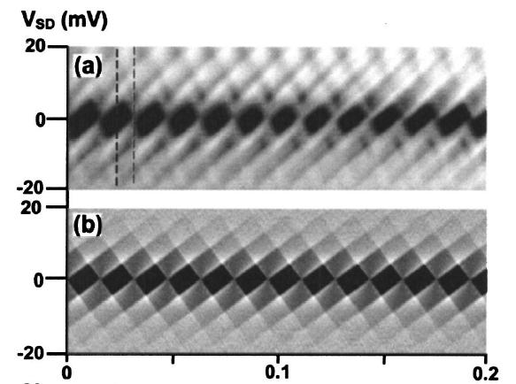
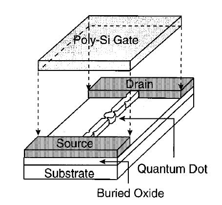
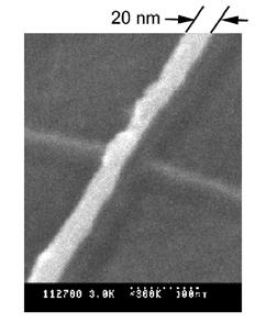
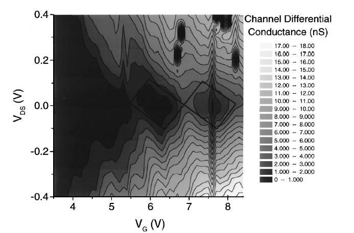
Formation of unintentional dots in small Si nanostructures
 Superlattices and Microstructures, Vol. 28, No. 5/6, 2000 doi:10.1006/spmi.2000.0942 Available online at http://www.idealibrary.com on Formation of unintentional dots in small Si nanostructures L. P. ROKHINSON,
2) Atom manipulation. Xe / Ni(110) Model: Experiment:
 Atom manipulation. Xe / Ni(110) Model: Experiment:") 2) Atom manipulation D. Eigler & E. Schweizer, Nature 344, 524 (1990) Xe / Ni(110) Model: Experiment: G.Meyer, et al. Applied Physics A 68, 125 (1999) First the tip is approached close to the adsorbate
2) Atom manipulation D. Eigler & E. Schweizer, Nature 344, 524 (1990) Xe / Ni(110) Model: Experiment: G.Meyer, et al. Applied Physics A 68, 125 (1999) First the tip is approached close to the adsorbate
Electrical and Optical Properties. H.Hofmann
 Introduction to Nanomaterials Electrical and Optical Properties H.Hofmann Electrical Properties Ohm: G= σw/l where is the length of the conductor, measured in meters [m], A is the cross-section area of
Final exam. Introduction to Nanotechnology. Name: Student number:
 1 Final exam. Introduction to Nanotechnology Name: Student number: 1. (a) What is the definition for a cluster size-wise? (3%) (b) Calculate the energy separation near the Fermi surface of a metallic cluster
chiral m = n Armchair m = 0 or n = 0 Zigzag m n Chiral Three major categories of nanotube structures can be identified based on the values of m and n
 zigzag armchair Three major categories of nanotube structures can be identified based on the values of m and n m = n Armchair m = 0 or n = 0 Zigzag m n Chiral Nature 391, 59, (1998) chiral J. Tersoff,
Carbon Nanotubes part 2 CNT s s as a toy model for basic science. Niels Bohr Institute School 2005
 Carbon Nanotubes part 2 CNT s s as a toy model for basic science Niels Bohr Institute School 2005 1 Carbon Nanotubes as a model system 2 Christian Schönenberger University of Basel B. Babic W. Belzig M.
Electrical Contacts to Carbon Nanotubes Down to 1nm in Diameter
 1 Electrical Contacts to Carbon Nanotubes Down to 1nm in Diameter Woong Kim, Ali Javey, Ryan Tu, Jien Cao, Qian Wang, and Hongjie Dai* Department of Chemistry and Laboratory for Advanced Materials, Stanford
How a single defect can affect silicon nano-devices. Ted Thorbeck
 How a single defect can affect silicon nano-devices Ted Thorbeck tedt@nist.gov The Big Idea As MOS-FETs continue to shrink, single atomic scale defects are beginning to affect device performance Gate Source
Electron counting with quantum dots
 Electron counting with quantum dots Klaus Ensslin Solid State Physics Zürich with S. Gustavsson I. Shorubalko R. Leturcq T. Ihn A. C. Gossard Time-resolved charge detection Single photon detection Time-resolved
Chapter 5 Nanomanipulation. Chapter 5 Nanomanipulation. 5.1: With a nanotube. Cutting a nanotube. Moving a nanotube
 Objective: learn about nano-manipulation techniques with a STM or an AFM. 5.1: With a nanotube Moving a nanotube Cutting a nanotube Images at large distance At small distance : push the NT Voltage pulse
Ideal Discrete Energy Levels in Synthesized Au. Nanoparticle for Chemically Assembled. Single-Electron Transistors
 Ideal Discrete Energy Levels in Synthesized Au Nanoparticle for Chemically Assembled Single-Electron Transistors Shinya Kano,, Yasuo Azuma,, Kosuke Maeda,, Daisuke Tanaka,, Masanori Sakamoto,,, Toshiharu
SUPPLEMENTARY INFORMATION
 Electrical control of single hole spins in nanowire quantum dots V. S. Pribiag, S. Nadj-Perge, S. M. Frolov, J. W. G. van den Berg, I. van Weperen., S. R. Plissard, E. P. A. M. Bakkers and L. P. Kouwenhoven
SUPPLEMENTARY INFORMATION
 Collapse of superconductivity in a hybrid tin graphene Josephson junction array by Zheng Han et al. SUPPLEMENTARY INFORMATION 1. Determination of the electronic mobility of graphene. 1.a extraction from
Single-Electron Devices
 Single-Electron Devices Jürgen Weis Max-Planck-Institut für Festkörperforschung, Heisenbergstr. 1, 7569 Stuttgart, Germany 1 Introduction The electrical charge is quantized in the elementary quantum e
Chapter 3 Properties of Nanostructures
 Chapter 3 Properties of Nanostructures In Chapter 2, the reduction of the extent of a solid in one or more dimensions was shown to lead to a dramatic alteration of the overall behavior of the solids. Generally,
SUPPLEMENTARY INFORMATION
 Simultaneous and coordinated rotational switching of all molecular rotors in a network Y. Zhang, H. Kersell, R. Stefak, J. Echeverria, V. Iancu, U. G. E. Perera, Y. Li, A. Deshpande, K.-F. Braun, C. Joachim,
FEW ELECTRON QUANTUM DOTS IN InAs/InP CORE SHELL NANOWIRES
 FEW ELECTRON QUANTUM DOTS IN InAs/InP CORE SHELL NANOWIRES By Shivendra Upadhyay Delft University of Technology Faculty of Applied Science Kavli Institute of Nanoscience Quantum Transport Group Drs. J.
Presented by: Göteborg University, Sweden
 SMR 1760-3 COLLEGE ON PHYSICS OF NANO-DEVICES 10-21 July 2006 Nanoelectromechanics of Magnetic and Superconducting Tunneling Devices Presented by: Robert Shekhter Göteborg University, Sweden * Mechanically
Charging and Kondo Effects in an Antidot in the Quantum Hall Regime
 Semiconductor Physics Group Cavendish Laboratory University of Cambridge Charging and Kondo Effects in an Antidot in the Quantum Hall Regime M. Kataoka C. J. B. Ford M. Y. Simmons D. A. Ritchie University
Introduction to Nanotechnology Chapter 5 Carbon Nanostructures Lecture 1
 Introduction to Nanotechnology Chapter 5 Carbon Nanostructures Lecture 1 ChiiDong Chen Institute of Physics, Academia Sinica chiidong@phys.sinica.edu.tw 02 27896766 Carbon contains 6 electrons: (1s) 2,
arxiv: v1 [cond-mat.mes-hall] 28 Jun 2008
![arxiv: v1 [cond-mat.mes-hall] 28 Jun 2008](/thumbs/95/122775440.jpg "arxiv: v1 [cond-mat.mes-hall] 28 Jun 2008") TOPICAL REVIEW arxiv:0806.4719v1 [cond-mat.mes-hall] 28 Jun 2008 Spin effects in single electron tunneling J. Barnaś 1,2 and I. Weymann 1 1 Department of Physics, Adam Mickiewicz University, 61-614 Poznań,
TOPICAL REVIEW arxiv:0806.4719v1 [cond-mat.mes-hall] 28 Jun 2008 Spin effects in single electron tunneling J. Barnaś 1,2 and I. Weymann 1 1 Department of Physics, Adam Mickiewicz University, 61-614 Poznań,
Quantum Noise Measurement of a Carbon Nanotube Quantum dot in the Kondo Regime
 Quantum Noise Measurement of a Carbon Nanotube Quantum dot in the Kondo Regime J. Basset, 1 A.Yu. Kasumov, 1 C.P. Moca, G. Zarand,, 3 P. Simon, 1 H. Bouchiat, 1 and R. Deblock 1 1 Laboratoire de Physique
Determination of the tunnel rates through a few-electron quantum dot
 Determination of the tunnel rates through a few-electron quantum dot R. Hanson 1,I.T.Vink 1, D.P. DiVincenzo 2, L.M.K. Vandersypen 1, J.M. Elzerman 1, L.H. Willems van Beveren 1 and L.P. Kouwenhoven 1
Chapter 4: Bonding in Solids and Electronic Properties. Free electron theory
 Chapter 4: Bonding in Solids and Electronic Properties Free electron theory Consider free electrons in a metal an electron gas. regards a metal as a box in which electrons are free to move. assumes nuclei
Experimental Studies of Single-Molecule Transistors
 Experimental Studies of Single-Molecule Transistors Dan Ralph group at Cornell University Janice Wynn Guikema Texas A&M University Condensed Matter Seminar January 18, 2006 p.1 Cornell Image from http://www.cornell.edu/
Three-terminal quantum-dot thermoelectrics
 Three-terminal quantum-dot thermoelectrics Björn Sothmann Université de Genève Collaborators: R. Sánchez, A. N. Jordan, M. Büttiker 5.11.2013 Outline Introduction Quantum dots and Coulomb blockade Quantum
Formation mechanism and Coulomb blockade effect in self-assembled gold quantum dots
 Formation mechanism and Coulomb blockade effect in self-assembled gold quantum dots S. F. Hu a) National Nano Device Laboratories, Hsinchu 300, Taiwan R. L. Yeh and R. S. Liu Department of Chemistry, National
Solid-State Spin Quantum Computers
 Solid-State Spin Quantum Computers 1 NV-Centers in Diamond P Donors in Silicon Kane s Computer (1998) P- doped silicon with metal gates Silicon host crystal + 31 P donor atoms + Addressing gates + J- coupling
Emerging Research Devices: A Study of CNTFET and SET as a replacement for SiMOSFET
 1 Emerging Research Devices: A Study of CNTFET and SET as a replacement for SiMOSFET Mahmoud Lababidi, Krishna Natarajan, Guangyu Sun Abstract Since the development of the Silicon MOSFET, it has been the
Large Storage Window in a-sinx/nc-si/a-sinx Sandwiched Structure
 2017 Asia-Pacific Engineering and Technology Conference (APETC 2017) ISBN: 978-1-60595-443-1 Large Storage Window in a-sinx/nc-si/a-sinx Sandwiched Structure Xiang Wang and Chao Song ABSTRACT The a-sin
EN2912C: Future Directions in Computing Lecture 08: Overview of Near-Term Emerging Computing Technologies
 EN2912C: Future Directions in Computing Lecture 08: Overview of Near-Term Emerging Computing Technologies Prof. Sherief Reda Division of Engineering Brown University Fall 2008 1 Near-term emerging computing
Kondo Physics in Nanostructures. A.Abdelrahman Department of Physics University of Basel Date: 27th Nov. 2006/Monday meeting
 Kondo Physics in Nanostructures A.Abdelrahman Department of Physics University of Basel Date: 27th Nov. 2006/Monday meeting Kondo Physics in Nanostructures Kondo Effects in Metals: magnetic impurities
Charge transport in nanoscale three-terminal devices. 1. Introduction: Three-terminal devices and quantization
 0 0 0 0 harge transport in nanoscale three-terminal devices J.M. Thijssen and H..J. van der Zant Kavli Institute of Nanoscience, elft University of Technology, Lorentzweg, J elft (The Netherlands). Abstract
Superconductivity at nanoscale
 Superconductivity at nanoscale Superconductivity is the result of the formation of a quantum condensate of paired electrons (Cooper pairs). In small particles, the allowed energy levels are quantized and
Metallic: 2n 1. +n 2. =3q Armchair structure always metallic = 2
 Properties of CNT d = 2.46 n 2 2 1 + n1n2 + n2 2π Metallic: 2n 1 +n 2 =3q Armchair structure always metallic a) Graphite Valence(π) and Conduction(π*) states touch at six points(fermi points) Carbon Nanotube:
Quantum dots. Quantum computing. What is QD. Invention QD TV. Complex. Lego. https://www.youtube.com/watch?v=ne819ppca5o
 Intel's New 49-qubit Quantum Chip & Neuromorphic Chip https://www.youtube.com/watch?v=ne819ppca5o How To Make a Quantum Bit https://www.youtube.com/watch?v=znzzggr2mhk Quantum computing https://www.youtube.com/watch?v=dxaxptlhqqq
Quasiadiabatic switching for metal-island quantum-dot cellular automata
 JOURNAL OF APPLIED PHYSICS VOLUME 85, NUMBER 5 1 MARCH 1999 Quasiadiabatic switching for metal-island quantum-dot cellular automata Géza Tóth and Craig S. Lent a) Department of Electrical Engineering,
arxiv:cond-mat/ v1 [cond-mat.mes-hall] 27 Nov 2001
![arxiv:cond-mat/ v1 [cond-mat.mes-hall] 27 Nov 2001](/thumbs/72/66784898.jpg "arxiv:cond-mat/ v1 [cond-mat.mes-hall] 27 Nov 2001") Published in: Single-Electron Tunneling and Mesoscopic Devices, edited by H. Koch and H. Lübbig (Springer, Berlin, 1992): pp. 175 179. arxiv:cond-mat/0111505v1 [cond-mat.mes-hall] 27 Nov 2001 Resonant
Published in: Single-Electron Tunneling and Mesoscopic Devices, edited by H. Koch and H. Lübbig (Springer, Berlin, 1992): pp. 175 179. arxiv:cond-mat/0111505v1 [cond-mat.mes-hall] 27 Nov 2001 Resonant
Tunneling transport. Courtesy Prof. S. Sawyer, RPI Also Davies Ch. 5
 unneling transport Courtesy Prof. S. Sawyer, RPI Also Davies Ch. 5 Electron transport properties l e : electronic mean free path l φ : phase coherence length λ F : Fermi wavelength ecture Outline Important
!"#"$#%&'(&)(*+,'#+-(."//+/,0( 1+#&-,#&'(1$#%&'(%'(2%/%$&'3&'3 %'4+/,#&0(."//4#
(*+,'#+-(.//+/,0( 1+#&-,#&'(1$#%&'(%'(2%/%$&'3&'3 %'4+/,#&0(.//4#") Università di Pisa!""$%&'(&)(*+,'+-(."//+/,0( 1+&-,&'(1$%&'(%'(2%/%$&'3&'3 %'4+/,&0(."//4 $%&'(()*+,+)% 4)6%?&)@0/&'A)./*0*/0?)%A0BBC./D'?@%E)'/0FGB0&&?'/),%+./D'?@%&),%+H0B0,'@-/),%E)'/)+ I/)J0?5)&KA)L)5%
Università di Pisa!""$%&'(&)(*+,'+-(."//+/,0( 1+&-,&'(1$%&'(%'(2%/%$&'3&'3 %'4+/,&0(."//4 $%&'(()*+,+)% 4)6%?&)@0/&'A)./*0*/0?)%A0BBC./D'?@%E)'/0FGB0&&?'/),%+./D'?@%&),%+H0B0,'@-/),%E)'/)+ I/)J0?5)&KA)L)5%
Counting Individual Electrons on Liquid Helium
 Counting Individual Electrons on Liquid Helium G. Papageorgiou 1, P. Glasson 1, K. Harrabi 1, V.Antonov 1, E.Collin 2, P.Fozooni 1, P.G.Frayne 1, M.J.Lea 1, Y.Mukharsky 2 and D.G.Rees 1. 1 Department of
Zeeman splitting of single semiconductor impurities in resonant tunneling heterostructures
 Superlattices and Microstructures, Vol. 2, No. 4, 1996 Zeeman splitting of single semiconductor impurities in resonant tunneling heterostructures M. R. Deshpande, J. W. Sleight, M. A. Reed, R. G. Wheeler
Supplementary Information
 Supplementary Information Quantum supercurrent transistors in carbon nanotubes Pablo Jarillo-Herrero, Jorden A. van Dam, Leo P. Kouwenhoven Device Fabrication The nanotubes were grown by chemical vapour
FABRICATION AND CHARACTERIZATION OF SINGLE ELECTRON DEVICE AND STUDY OF ENERGY FILTERING IN SINGLE ELECTRON TRANSPORT LIANG-CHIEH MA
 FABRICATION AND CHARACTERIZATION OF SINGLE ELECTRON DEVICE AND STUDY OF ENERGY FILTERING IN SINGLE ELECTRON TRANSPORT by LIANG-CHIEH MA Presented to the Faculty of the Graduate School of The University
No reason one cannot have double-well structures: With MBE growth, can control well thicknesses and spacings at atomic scale.
 The story so far: Can use semiconductor structures to confine free carriers electrons and holes. Can get away with writing Schroedinger-like equation for Bloch envelope function to understand, e.g., -confinement
Electrical Control of Single Spins in Semiconductor Quantum Dots Jason Petta Physics Department, Princeton University
 Electrical Control of Single Spins in Semiconductor Quantum Dots Jason Petta Physics Department, Princeton University g Q 2 m T + S Mirror U 3 U 1 U 2 U 3 Mirror Detector See Hanson et al., Rev. Mod. Phys.
Few-electron molecular states and their transitions in a single InAs quantum dot molecule
 Few-electron molecular states and their transitions in a single InAs quantum dot molecule T. Ota 1*, M. Rontani 2, S. Tarucha 1,3, Y. Nakata 4, H. Z. Song 4, T. Miyazawa 4, T. Usuki 4, M. Takatsu 4, and
Terahertz sensing and imaging based on carbon nanotubes:
 Terahertz sensing and imaging based on carbon nanotubes: Frequency-selective detection and near-field imaging Yukio Kawano RIKEN, JST PRESTO ykawano@riken.jp http://www.riken.jp/lab-www/adv_device/kawano/index.html
Manipulation of Majorana fermions via single charge control
 Manipulation of Majorana fermions via single charge control Karsten Flensberg Niels Bohr Institute University of Copenhagen Superconducting hybrids: from conventional to exotic, Villard de Lans, France,
ECE 305: Fall MOSFET Energy Bands
 ECE 305: Fall 2016 MOSFET Energy Bands Professor Peter Bermel Electrical and Computer Engineering Purdue University, West Lafayette, IN USA pbermel@purdue.edu Pierret, Semiconductor Device Fundamentals
Majorana single-charge transistor. Reinhold Egger Institut für Theoretische Physik
 Majorana single-charge transistor Reinhold Egger Institut für Theoretische Physik Overview Coulomb charging effects on quantum transport through Majorana nanowires: Two-terminal device: Majorana singlecharge
Self-assembled SiGe single hole transistors
 Self-assembled SiGe single hole transistors G. Katsaros 1, P. Spathis 1, M. Stoffel 2, F. Fournel 3, M. Mongillo 1, V. Bouchiat 4, F. Lefloch 1, A. Rastelli 2, O. G. Schmidt 2 and S. De Franceschi 1 1
(a) (b) Supplementary Figure 1. (a) (b) (a) Supplementary Figure 2. (a) (b) (c) (d) (e)
 (b) Supplementary Figure 1. (a) (b) (a) Supplementary Figure 2. (a) (b) (c) (d) (e)") (a) (b) Supplementary Figure 1. (a) An AFM image of the device after the formation of the contact electrodes and the top gate dielectric Al 2 O 3. (b) A line scan performed along the white dashed line
(a) (b) Supplementary Figure 1. (a) An AFM image of the device after the formation of the contact electrodes and the top gate dielectric Al 2 O 3. (b) A line scan performed along the white dashed line
Supplementary Figure S1. AFM images of GraNRs grown with standard growth process. Each of these pictures show GraNRs prepared independently,
 Supplementary Figure S1. AFM images of GraNRs grown with standard growth process. Each of these pictures show GraNRs prepared independently, suggesting that the results is reproducible. Supplementary Figure
introduction: what is spin-electronics?
 Spin-dependent transport in layered magnetic metals Patrick Bruno Max-Planck-Institut für Mikrostrukturphysik, Halle, Germany Summary: introduction: what is spin-electronics giant magnetoresistance (GMR)
M.C. Escher. Angels and devils (detail), 1941
, 1941") M.C. Escher Angels and devils (detail), 1941 1 Coherent Quantum Phase Slip: Exact quantum dual to Josephson Tunneling (Coulomb blockade is a partial dual) Degree of freedom in superconductor: Phase and
M.C. Escher Angels and devils (detail), 1941 1 Coherent Quantum Phase Slip: Exact quantum dual to Josephson Tunneling (Coulomb blockade is a partial dual) Degree of freedom in superconductor: Phase and
Supplementary figures
 Supplementary figures Supplementary Figure 1. A, Schematic of a Au/SRO113/SRO214 junction. A 15-nm thick SRO113 layer was etched along with 30-nm thick SRO214 substrate layer. To isolate the top Au electrodes
Supplementary Information for Pseudospin Resolved Transport Spectroscopy of the Kondo Effect in a Double Quantum Dot. D2 V exc I
 Supplementary Information for Pseudospin Resolved Transport Spectroscopy of the Kondo Effect in a Double Quantum Dot S. Amasha, 1 A. J. Keller, 1 I. G. Rau, 2, A. Carmi, 3 J. A. Katine, 4 H. Shtrikman,
The Physics of Nanoelectronics
 The Physics of Nanoelectronics Transport and Fluctuation Phenomena at Low Temperatures Tero T. Heikkilä Low Temperature Laboratory, Aalto University, Finland OXFORD UNIVERSITY PRESS Contents List of symbols