Thermal Oxidation of Si
|
|
|
- Ethan Farmer
- 6 years ago
- Views:
Transcription

1 Thermal Oxidation of General Properties of O 2 Applications of thermal O 2 Deal-Grove Model of Oxidation Thermal O 2 is amorphous. Weight Density = 2.20 gm/cm 3 Molecular Density = 2.3E22 molecules/cm 3 O2 <> Crystalline O 2 [Quartz] = 2.65 gm/cm 3
2 Thermal O 2 Properties () Excellent Electrical Insulator Resistivity > E20 ohm-cm Energy Gap ~ 9 ev (2) High Breakdown Electric Field > 0MV/cm (3) Stable and Reproducible /O 2 Interface (4) Conformal ide growth on exposed surface Thermal Oxidation O2 2
3 (5) O 2 is a good diffusion mask for common dopants D Thermal O 2 Properties cont. D sio << e.g. B, P, As, Sb. 2 si O 2 *exceptions are are Ga Ga (a (a p-type dopant) and and some metals, e.g. e.g. Cu, Cu, Au Au (6) Very good etching selectivity between and O 2. O 2 HF dip 3
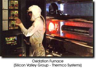
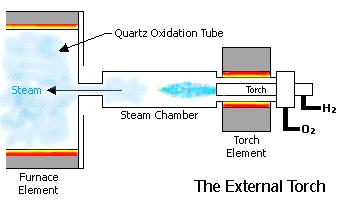
4 Steam generation for wet idation 4
5 Thickness of consumed during idation original surface O 2 X si X X si = X N N si molecular density of O2 atomic density of 22 3 = X = X molecules / cm atoms / cm 5
6 For -dimensional planar ide growth µm idized 2.7 µm O 2 Suggested calculation exercise: µm diameter sphere completely idized.3 µm diameter O 2 sphere O2 6
7 Kinetics of O 2 Growth Oxidant Flow (O 2 or H 2 O) Gas Diffusion Solid-state Diffusion O 2 Formation Gas Flow Stagnant Layer O 2 -Substrate 7
8 Deal-Grove Model C G stagnant layer C s O 2 Note C ss C o C o C i X 0x F F 2 F 3 gas transport flux diffusion flux through O 2 reaction flux at interface 8
9 F = h C C F 2 F = D 3 = ( ) G G S C x C D k C s i Mass transfer coefficient [cm/sec]. o X C i Fick s Law of Solid-state Diffusion Diffusivity [cm 2 /sec] Surface reaction rate constant [cm/sec] Comment: The derivation used in Jaeger textbook assumes F is large (not a rate-limiting factor for growth rate). Hence, the algebra looks simpler. However, the lecture notes derivation includes gas transport effect and can be directly applied to CVD growth rate which will be discussed in later weeks. 9
10 How to solve the idant concentrations? C S and C o are related by Henry s Law C G is a controlled process variable (proportional to the input idant gas pressure) Only C o and C i i are the 2 unknown variables which can be be solved from the steady-state condition: F = F 2 =F =F 3 (( 2 equations) 0
11 Derivation of Oxidation Growth Rate C = H P o s Henry s Law Henry s constant partial pressure of idant at surface [in gaseous form]. = H ( kt C ) s from ideal gas law PV= NkT C s = C o HkT
12 Derivation of Oxidation Growth Rate cont. Define C A F can be re-written as: h F = G HkT ( C C A o ) h ( HkT C G Using the steady-state condition: ) This is a control process variable. For a given idant pressure, C A is known. Conservation of mass flux F = = F F equations to to solve the 2 unknowns: C o & C i i 2
13 Derivation of Oxidation Growth Rate cont. Therefore C i = C k + + h A kx D s s C k = + s X Ci D o F ( = F = F = F ) 2 3 = k s C i = + k k s h C k + s A s X D 3
14 Now, convert F into Oxide Thickness Growth Rate F = N dx dt X Oxidant molecules/unit volume required to form a unit volume of O 2. O 2 F { t} Therefore, we have the ide growth rate eqn: N dx dt = + k k s h C A k + s s X D 4
15 Initial Condition: At t = 0, X = X i O 2 O 2 x Solution X 2 + AX = B( t +τ ) A B 2D( k 2 DC N s A + h ) Note: h >>k s for typical idation condition τ = X 2 i + AX B i 5
16 Note : dry and wet idation have different N factors N N 22 3 = / cm for O 2 as idant + O O = / cm for H 2 O as idant + 2H O O + 2H
17 X Summary of Deal-Grove Model t X 2 X 2 t + AX dx dt 0 x + = A B ( t dx dt + τ ) = B t dx dt = A B + 2X Oxide Growth Rate slows down with with increase of of ide thickness 7
18 A X = + 2 t+ τ A 2 4 B (Case ) Large t [ large X ] X Bt (Case 2) Small t [ Small X ] X B A t 8
19 Deal-Grove Model Parameters () 2 D C B A N D D e Q kt Q = activation energy for diffusion (2) B A = ( h + k s ) C N A k s e ' Q kt Q = activation energy for interface reaction For thermal idation of of,, h is is typically >> >> k s s B/A is is k s s (i.e. F is is rarely the rate-limiting step) 9
20 B = Parabolic Constant B/A = Linear Constant 20
21 Oxidation Charts The The charts are are based on on X i = i 0!! 2
22 Two Ways to Calculate Oxide Thickness Grown by Thermal Oxidation E.g. O 2 x i= 4000A 00 o C 33min steam O 2 x o x Method : Find B & B/A from Charts Solve X 2 + AX = B( t +τ ) 22
23 Method 2: Use Oxidation Charts 6500 o A 4000 o A Two Ways to Calculate Oxide Thickness Grown by Thermal Oxidation X 00 o C T 3 T 2 T The The charts are are based on on X i =0 i =0!! X i = 4000 A τ = 24 min Total effective idation time ( 24 33) min = 57min time(min) at 00 o C from chart + if start with = 0 X i 23
24 () Grown at 000 o C, 5hrs (3) CVD Oxide O o A x i O o A CVD Oxide (2) Grown at 00 o C, 24min O o A For same X i, i τ is the same for all three cases shown here 24
Oxidation of Si. Why spend a whole lecture on oxidation of Si? GaAs has high m and direct band no oxide
 Oxidation of Why spend a whole lecture on oxidation of? Ge has high m e, m h, Ge stable but no oxide GaAs has high m and direct band no oxide e Why? is stable down to 10-9 Torr, T > 900 C can be etched
Lecture 7 Oxidation. Chapter 7 Wolf and Tauber. ECE611 / CHE611 Electronic Materials Processing Fall John Labram 1/82
 Lecture 7 Oxidation Chapter 7 Wolf and Tauber 1/82 Announcements Homework: Homework will be returned to you today (please collect from me at front of class). Solutions will be also posted online on today
Diffusion. Diffusion = the spontaneous intermingling of the particles of two or more substances as a result of random thermal motion
 Diffusion Diffusion = the spontaneous intermingling of the particles of two or more substances as a result of random thermal motion Fick s First Law Γ ΔN AΔt Γ = flux ΔN = number of particles crossing
Oxide growth model. Known as the Deal-Grove or linear-parabolic model
 Oxide growth model Known as the Deal-Grove or linear-parabolic model Important elements of the model: Gas molecules (oxygen or water) are incident on the surface of the wafer. Molecules diffuse through
EE143 Fall 2016 Microfabrication Technologies. Lecture 6: Thin Film Deposition Reading: Jaeger Chapter 6
 EE143 Fall 2016 Microfabrication Technologies Lecture 6: Thin Film Deposition Reading: Jaeger Chapter 6 Prof. Ming C. Wu wu@eecs.berkeley.edu 511 Sutardja Dai Hall (SDH) 1 Vacuum Basics Units 1 atmosphere
EE 143 Microfabrication Technology Fall 2014
 EE 143 Microfabrication Technology Fall 2014 Prof. Clark T.-C. Nguyen Dept. of Electrical Engineering & Computer Sciences University of California at Berkeley Berkeley, CA 94720 EE 143: Microfabrication
Make sure the exam paper has 7 pages (including cover page) + 3 pages of data for reference
 + 3 pages of data for reference") UNIVERSITY OF CALIFORNIA College of Engineering Department of Electrical Engineering and Computer Sciences Fall 2005 EE143 Midterm Exam #1 Family Name First name SID Signature Make sure the exam paper
UNIVERSITY OF CALIFORNIA College of Engineering Department of Electrical Engineering and Computer Sciences Fall 2005 EE143 Midterm Exam #1 Family Name First name SID Signature Make sure the exam paper
Fabrication Technology, Part I
 EEL5225: Principles of MEMS Transducers (Fall 2004) Fabrication Technology, Part I Agenda: Microfabrication Overview Basic semiconductor devices Materials Key processes Oxidation Thin-film Deposition Reading:
3.155J/6.152J Microelectronic Processing Technology Fall Term, 2004
 3.155J/6.152J Microelectronic Processing Technology Fall Term, 2004 Bob O'Handley Martin Schmidt Quiz Nov. 17, 2004 Ion implantation, diffusion [15] 1. a) Two identical p-type Si wafers (N a = 10 17 cm
Section 7: Diffusion. Jaeger Chapter 4. EE143 Ali Javey
 Section 7: Diffusion Jaeger Chapter 4 Surface Diffusion: Dopant Sources (a) Gas Source: AsH 3, PH 3, B 2 H 6 (b) Solid Source BN Si BN Si (c) Spin-on-glass SiO 2 +dopant oxide (d) Liquid Source. Fick s
Make sure the exam paper has 9 pages (including cover page) + 3 pages of data for reference
 + 3 pages of data for reference") UNIVERSITY OF CALIFORNIA College of Engineering Department of Electrical Engineering and Computer Sciences Spring 2006 EE143 Midterm Exam #1 Family Name First name SID Signature Make sure the exam paper
UNIVERSITY OF CALIFORNIA College of Engineering Department of Electrical Engineering and Computer Sciences Spring 2006 EE143 Midterm Exam #1 Family Name First name SID Signature Make sure the exam paper
CVD: General considerations.
 CVD: General considerations. PVD: Move material from bulk to thin film form. Limited primarily to metals or simple materials. Limited by thermal stability/vapor pressure considerations. Typically requires
Semiconductors Reference: Chapter 4 Jaeger or Chapter 3 Ruska Recall what determines conductor, insulator and semiconductor Plot the electron energy
 Semiconductors Reference: Chapter 4 Jaeger or Chapter 3 Ruska Recall what determines conductor, insulator and semiconductor Plot the electron energy states of a material In some materials get the creation
Xing Sheng, 微纳光电子材料与器件工艺原理. Doping 掺杂. Xing Sheng 盛兴. Department of Electronic Engineering Tsinghua University
 微纳光电子材料与器件工艺原理 Doping 掺杂 Xing Sheng 盛兴 Department of Electronic Engineering Tsinghua University xingsheng@tsinghua.edu.cn 1 Semiconductor PN Junctions Xing Sheng, EE@Tsinghua LEDs lasers detectors solar
Dopant Diffusion. (1) Predeposition dopant gas. (2) Drive-in Turn off dopant gas. dose control. Doped Si region
 Predeposition dopant gas. (2) Drive-in Turn off dopant gas. dose control. Doped Si region") Dopant Diffusion (1) Predeposition dopant gas dose control SiO Si SiO Doped Si region () Drive-in Turn off dopant gas or seal surface with oxide profile control (junction depth; concentration) SiO SiO
Dopant Diffusion (1) Predeposition dopant gas dose control SiO Si SiO Doped Si region () Drive-in Turn off dopant gas or seal surface with oxide profile control (junction depth; concentration) SiO SiO
Self-study problems and questions Processing and Device Technology, FFF110/FYSD13
 Self-study problems and questions Processing and Device Technology, FFF110/FYSD13 Version 2016_01 In addition to the problems discussed at the seminars and at the lectures, you can use this set of problems
Diffusion and Ion implantation Reference: Chapter 4 Jaeger or Chapter 3 Ruska N & P Dopants determine the resistivity of material Note N lower
 Diffusion and Ion implantation Reference: Chapter 4 Jaeger or Chapter 3 Ruska N & P Dopants determine the resistivity of material Note N lower resistavity than p: due to higher carrier mobility Near linear
UNIVERSITY OF CALIFORNIA. College of Engineering. Department of Electrical Engineering and Computer Sciences. Professor Ali Javey.
 UNIVERSITY OF CALIFORNIA College of Engineering Department of Electrical Engineering and Computer Sciences EE 143 Professor Ali Javey Spring 2009 Exam 2 Name: SID: Closed book. One sheet of notes is allowed.
Chapter 3 Engineering Science for Microsystems Design and Fabrication
 Lectures on MEMS and MICROSYSTEMS DESIGN and MANUFACTURE Chapter 3 Engineering Science for Microsystems Design and Fabrication In this Chapter, we will present overviews of the principles of physical and
ECE611 / CHE611: Electronic Materials Processing Fall 2017 John Labram Solutions to Homework 2 Due at the beginning of class Thursday October 19 th
 ECE611 / CHE611: Electronic Materials Processing Fall 017 John Labram Solutions to Homework Due at the beginning of class Thursday October 19 th Question 1 [3 marks]: a) Piranha solution consists of a
EE143 LAB. Professor N Cheung, U.C. Berkeley
 EE143 LAB 1 1 EE143 Equipment in Cory 218 2 Guidelines for Process Integration * A sequence of Additive and Subtractive steps with lateral patterning Processing Steps Si wafer Watch out for materials compatibility
produced a sputter rate of 0.9 nm/s for the radially profiled, un-etched wires. A slightly
 Supporting Information: Beam Current and Sputtering Rate: Using a 16 kev Cs + primary ion beam and a 1 µm 2 rastered area, a 10 pa beam current produced a sputter rate of 0.9 nm/s for the radially profiled,
ECE 416/516 IC Technologies
 ECE 46/56 IC Technologies Professor James E. Morris Spring 0 Chapter 4 Thermal Oxidation THERMAL OXIDATION Basic Concepts SiO and the Si/SiO interface are the principal reasons for silicon s dominance
LECTURE 5 SUMMARY OF KEY IDEAS
 LECTURE 5 SUMMARY OF KEY IDEAS Etching is a processing step following lithography: it transfers a circuit image from the photoresist to materials form which devices are made or to hard masking or sacrificial
Section 3: Etching. Jaeger Chapter 2 Reader
 Section 3: Etching Jaeger Chapter 2 Reader Etch rate Etch Process - Figures of Merit Etch rate uniformity Selectivity Anisotropy d m Bias and anisotropy etching mask h f substrate d f d m substrate d f
Section 5: Thin Film Deposition part 1 : sputtering and evaporation. Jaeger Chapter 6. EE143 Ali Javey
 Section 5: Thin Film Deposition part 1 : sputtering and evaporation Jaeger Chapter 6 Vacuum Basics 1. Units 1 atmosphere = 760 torr = 1.013x10 5 Pa 1 bar = 10 5 Pa = 750 torr 1 torr = 1 mm Hg 1 mtorr =
Dopant and Self-Diffusion in Semiconductors: A Tutorial
 Dopant and Self-Diffusion in Semiconductors: A Tutorial Eugene Haller and Hughes Silvestri MS&E, UCB and LBNL FLCC Tutorial 1/26/04 1 FLCC Outline Motivation Background Fick s Laws Diffusion Mechanisms
Lecture 18 Molecular Motion and Kinetic Energy
 Physical Principles in Biology Biology 3550 Fall 2017 Lecture 18 Molecular Motion and Kinetic Energy Monday, 2 October c David P. Goldenberg University of Utah goldenberg@biology.utah.edu Fick s First
EE 212 FALL ION IMPLANTATION - Chapter 8 Basic Concepts
 EE 212 FALL 1999-00 ION IMPLANTATION - Chapter 8 Basic Concepts Ion implantation is the dominant method of doping used today. In spite of creating enormous lattice damage it is favored because: Large range
Lecture 6 Plasmas. Chapters 10 &16 Wolf and Tauber. ECE611 / CHE611 Electronic Materials Processing Fall John Labram 1/68
 Lecture 6 Plasmas Chapters 10 &16 Wolf and Tauber 1/68 Announcements Homework: Homework will be returned to you on Thursday (12 th October). Solutions will be also posted online on Thursday (12 th October)
Make sure the exam paper has 8 pages plus an appendix page at the end.
 UNIVERSITY OF CALIFORNIA College of Engineering Deartment of Electrical Engineering and Comuter Sciences Fall 2000 EE143 Midterm Exam #1 Family Name First name Signature Make sure the exam aer has 8 ages
EE C245 ME C218 Introduction to MEMS Design Fall 2007
 EE C245 ME C218 Introduction to MEMS Design Fall 2007 Prof. Clark T.-C. Nguyen Dept. of Electrical Engineering & Computer Sciences University of California at Berkeley Berkeley, CA 94720 Lecture 4: Film
Lecture 150 Basic IC Processes (10/10/01) Page ECE Analog Integrated Circuits and Systems P.E. Allen
 Page ECE Analog Integrated Circuits and Systems P.E. Allen") Lecture 150 Basic IC Processes (10/10/01) Page 1501 LECTURE 150 BASIC IC PROCESSES (READING: TextSec. 2.2) INTRODUCTION Objective The objective of this presentation is: 1.) Introduce the fabrication of
Lecture 150 Basic IC Processes (10/10/01) Page 1501 LECTURE 150 BASIC IC PROCESSES (READING: TextSec. 2.2) INTRODUCTION Objective The objective of this presentation is: 1.) Introduce the fabrication of
UNIVERSITY OF CALIFORNIA College of Engineering Department of Electrical Engineering and Computer Sciences. Fall Exam 1
 UNIVERSITY OF CALIFORNIA College of Engineering Department of Electrical Engineering and Computer Sciences EECS 143 Fall 2008 Exam 1 Professor Ali Javey Answer Key Name: SID: 1337 Closed book. One sheet
Lecture 10 Thin Film Growth
 Lecture 10 Thin Film Growth 1/76 Announcements Homework: Homework Number 2 is returned today, please pick it up from me at the end of the class. Solutions are online. Homework 3 will be set Thursday (2
DIFFUSION - Chapter 7
 DIFFUSION - Chapter 7 Doping profiles determine many short-channel characteristics in MOS devices. Resistance impacts drive current. Scaling implies all lateral and vertical dimensions scale by the same
Ion Implantation ECE723
 Ion Implantation Topic covered: Process and Advantages of Ion Implantation Ion Distribution and Removal of Lattice Damage Simulation of Ion Implantation Range of Implanted Ions Ion Implantation is the
ION IMPLANTATION - Chapter 8 Basic Concepts
 ION IMPLANTATION - Chapter 8 Basic Concepts Ion implantation is the dominant method of doping used today. In spite of creating enormous lattice damage it is favored because: Large range of doses - 1 11
Size-dependent Metal-insulator Transition Random Materials Crystalline & Amorphous Purely Electronic Switching
 Nanometallic RRAM I-Wei Chen Department of Materials Science and Engineering University of Pennsylvania Philadelphia, PA 19104 Nature Nano, 6, 237 (2011) Adv Mater,, 23, 3847 (2011) Adv Func Mater,, 22,
Dopant Diffusion Sources
 Dopant Diffusion (1) Predeposition dopant gas dose control SiO Si SiO Doped Si region () Drive-in Turn off dopant gas or seal surface with oide profile control (junction depth; concentration) SiO SiO Si
Quiz #1 Practice Problem Set
 Name: Student Number: ELEC 3908 Physical Electronics Quiz #1 Practice Problem Set? Minutes January 22, 2016 - No aids except a non-programmable calculator - All questions must be answered - All questions
EE115C Winter 2017 Digital Electronic Circuits. Lecture 3: MOS RC Model, CMOS Manufacturing
 EE115C Winter 2017 Digital Electronic Circuits Lecture 3: MOS RC Model, CMOS Manufacturing Agenda MOS Transistor: RC Model (pp. 104-113) S R on D CMOS Manufacturing Process (pp. 36-46) S S C GS G G C GD
nmos IC Design Report Module: EEE 112
 nmos IC Design Report Author: 1302509 Zhao Ruimin Module: EEE 112 Lecturer: Date: Dr.Zhao Ce Zhou June/5/2015 Abstract This lab intended to train the experimental skills of the layout designing of the
Etching Issues - Anisotropy. Dry Etching. Dry Etching Overview. Etching Issues - Selectivity
 Etching Issues - Anisotropy Dry Etching Dr. Bruce K. Gale Fundamentals of Micromachining BIOEN 6421 EL EN 5221 and 6221 ME EN 5960 and 6960 Isotropic etchants etch at the same rate in every direction mask
Semiconductor Integrated Process Design (MS 635)
") Semiconductor Integrated Process Design (MS 635) Instructor: Prof. Keon Jae Lee - Office: 응용공학동 #4306, Tel: #3343 - Email: keonlee@kaist.ac.kr Lecture: (Tu, Th), 1:00-2:15 #2425 Office hour: Tues & Thur
Semiconductor Integrated Process Design (MS 635) Instructor: Prof. Keon Jae Lee - Office: 응용공학동 #4306, Tel: #3343 - Email: keonlee@kaist.ac.kr Lecture: (Tu, Th), 1:00-2:15 #2425 Office hour: Tues & Thur
Properties of Error Function erf(z) And Complementary Error Function erfc(z)
 And Complementary Error Function erfc(z)") Properties of Error Function erf(z) And Complementary Error Function erfc(z) z erf (z) π e -y dy erfc (z) 1 - erf (z) erf () erf( ) 1 erf(- ) - 1 erf (z) d erf(z) dz π z for z
Properties of Error Function erf(z) And Complementary Error Function erfc(z) z erf (z) π e -y dy erfc (z) 1 - erf (z) erf () erf( ) 1 erf(- ) - 1 erf (z) d erf(z) dz π z for z
UNIVERSITY OF CALIFORNIA College of Engineering Department of Electrical Engineering and Computer Sciences. Professor Chenming Hu.
 UNIVERSITY OF CALIFORNIA College of Engineering Department of Electrical Engineering and Computer Sciences EECS 130 Spring 2009 Professor Chenming Hu Midterm I Name: Closed book. One sheet of notes is
Plasma Deposition (Overview) Lecture 1
 Lecture 1") Plasma Deposition (Overview) Lecture 1 Material Processes Plasma Processing Plasma-assisted Deposition Implantation Surface Modification Development of Plasma-based processing Microelectronics needs (fabrication
Plasma Deposition (Overview) Lecture 1 Material Processes Plasma Processing Plasma-assisted Deposition Implantation Surface Modification Development of Plasma-based processing Microelectronics needs (fabrication
Chemical Vapor Deposition (CVD)
") Chemical Vapor Deposition (CVD) source chemical reaction film substrate More conformal deposition vs. PVD t Shown here is 100% conformal deposition ( higher temp has higher surface diffusion) t step 1
Chemical Vapor Deposition (CVD) source chemical reaction film substrate More conformal deposition vs. PVD t Shown here is 100% conformal deposition ( higher temp has higher surface diffusion) t step 1
Lecture 5: Diffusion Controlled Growth
 Materials Science & Metallurgy Master of Philosophy, Materials Modelling, Course MP6, Kinetics and Microstructure Modelling, H. K.. H. Bhadeshia Lecture 5: iffusion Controlled Growth Rate Controlling Processes
Microelectronic Device Fabrication I. Physics 445/545. David R. Evans
 Microelectronic Device Fabrication I (Basic Chemistry and Physics of Semiconductor Device Fabrication) Physics 445/545 David R. Evans Atomic Orbitals s-orbitals p-orbitals d-orbitals Chemical Bonding *
Introduction to Partial Differential Equations
 Introduction to Partial Differential Equations Philippe B. Laval KSU Current Semester Philippe B. Laval (KSU) 1D Heat Equation: Derivation Current Semester 1 / 19 Introduction The derivation of the heat
Solid State Physics SEMICONDUCTORS - IV. Lecture 25. A.H. Harker. Physics and Astronomy UCL
 Solid State Physics SEMICONDUCTORS - IV Lecture 25 A.H. Harker Physics and Astronomy UCL 9.9 Carrier diffusion and recombination Suppose we have a p-type semiconductor, i.e. n h >> n e. (1) Create a local
Session 0: Review of Solid State Devices. From Atom to Transistor
 Session 0: Review of Solid State Devices From Atom to Transistor 1 Objective To Understand: how Diodes, and Transistors operate! p n p+ n p- n+ n+ p 2 21 Century Alchemy! Ohm s law resistivity Resistivity
ETCHING Chapter 10. Mask. Photoresist
 ETCHING Chapter 10 Mask Light Deposited Substrate Photoresist Etch mask deposition Photoresist application Exposure Development Etching Resist removal Etching of thin films and sometimes the silicon substrate
EE 527 MICROFABRICATION. Lecture 24 Tai-Chang Chen University of Washington
 EE 527 MICROFABRICATION Lecture 24 Tai-Chang Chen University of Washington EDP ETCHING OF SILICON - 1 Ethylene Diamine Pyrocatechol Anisotropy: (100):(111) ~ 35:1 EDP is very corrosive, very carcinogenic,
Chapter 7. Solar Cell
 Chapter 7 Solar Cell 7.0 Introduction Solar cells are useful for both space and terrestrial application. Solar cells furnish the long duration power supply for satellites. It converts sunlight directly
Heat Removal of a Protection Chip after Surge Pulse Tom Graf Hochschule Luzern T&A Technikumstrasse 21 CH-6048 Horw Switzerland
 Heat Removal of a Protection Chip after Surge Pulse Tom Graf Hochschule Luzern T&A Technikumstrasse 21 CH-6048 Horw Switzerland 1 / 23 Abstract EMC protection elements experienced significant heating after
Reactive Ion Etching (RIE)
") Reactive Ion Etching (RIE) RF 13.56 ~ MHz plasma Parallel-Plate Reactor wafers Sputtering Plasma generates (1) Ions (2) Activated neutrals Enhance chemical reaction 1 2 Remote Plasma Reactors Plasma Sources
Reactive Ion Etching (RIE) RF 13.56 ~ MHz plasma Parallel-Plate Reactor wafers Sputtering Plasma generates (1) Ions (2) Activated neutrals Enhance chemical reaction 1 2 Remote Plasma Reactors Plasma Sources
Lecture 4. Ultrahigh Vacuum Science and Technology
 Lecture 4 Ultrahigh Vacuum Science and Technology Why do we need UHV? 1 Atmosphere = 760 torr; 1 torr = 133 Pa; N ~ 2.5 10 19 molecules/cm 3 Hertz-Knudsen equation p ZW 1/ 2 ( 2mk T) At p = 10-6 Torr it
Lecture 1. OUTLINE Basic Semiconductor Physics. Reading: Chapter 2.1. Semiconductors Intrinsic (undoped) silicon Doping Carrier concentrations
 silicon Doping Carrier concentrations") Lecture 1 OUTLINE Basic Semiconductor Physics Semiconductors Intrinsic (undoped) silicon Doping Carrier concentrations Reading: Chapter 2.1 EE105 Fall 2007 Lecture 1, Slide 1 What is a Semiconductor? Low
Lecture 1 OUTLINE Basic Semiconductor Physics Semiconductors Intrinsic (undoped) silicon Doping Carrier concentrations Reading: Chapter 2.1 EE105 Fall 2007 Lecture 1, Slide 1 What is a Semiconductor? Low
EE-612: Lecture 22: CMOS Process Steps
 EE-612: Lecture 22: CMOS Process Steps Mark Lundstrom Electrical and Computer Engineering Purdue University West Lafayette, IN USA Fall 2006 NCN www.nanohub.org Lundstrom EE-612 F06 1 outline 1) Unit Process
The goal of this project is to enhance the power density and lowtemperature efficiency of solid oxide fuel cells (SOFC) manufactured by atomic layer
 manufactured by atomic layer") Stanford University Michael Shandalov1, Shriram Ramanathan2, Changhyun Ko2 and Paul McIntyre1 1Department of Materials Science and Engineering, Stanford University 2Division of Engineering and Applied
Stanford University Michael Shandalov1, Shriram Ramanathan2, Changhyun Ko2 and Paul McIntyre1 1Department of Materials Science and Engineering, Stanford University 2Division of Engineering and Applied
Lecture 29: Kinetics of Oxidation of Metals: Part 2: Wagner Parabolic
 Lecture 9: Kinetics of Oxidat of Metals: Part : Wagner Parabolic Mod Today s topics Oxidat of metals: controlled by both the ic diffus (carried by M + and O - ) and the ectronic diffus (carried by e -
Electronics The basics of semiconductor physics
 Electronics The basics of semiconductor physics Prof. Márta Rencz, Gergely Nagy BME DED September 16, 2013 The basic properties of semiconductors Semiconductors conductance is between that of conductors
Vacuum Technology and film growth. Diffusion Resistor
 Vacuum Technology and film growth Poly Gate pmos Polycrystaline Silicon Source Gate p-channel Metal-Oxide-Semiconductor (MOSFET) Drain polysilicon n-si ion-implanted Diffusion Resistor Poly Si Resistor
Biology 3550 Physical Principles in Biology Fall Semester 2017 Mid-Term Exam 6 October 2017
 100 points total Please write your name on each page. In your answers you should: Biology 3550 Physical Principles in Biology Fall Semester 2017 Mid-Term Exam 6 October 2017 Show your work or provide an
Oxidation of hydrogenated crystalline silicon as an alternative approach for ultrathin SiO 2 growth
 Institute of Physics Publishing Journal of Physics: Conference Series 10 (2005) 246 250 doi:10.1088/1742-6596/10/1/061 Second Conference on Microelectronics, Microsystems and Nanotechnology Oxidation of
Lecture 2. Introduction to semiconductors Structures and characteristics in semiconductors
 Lecture 2 Introduction to semiconductors Structures and characteristics in semiconductors Semiconductor p-n junction Metal Oxide Silicon structure Semiconductor contact Literature Glen F. Knoll, Radiation
MATHEMATICS OF DOPING PROFILES. C(x,t) t. = D 2 C(x,t) x 2. 4Dt dx '
 t. = D 2 C(x,t) x 2. 4Dt dx '") EE43 MATHEMATICS OF DOPING PROFILES N. Cheung The diffusion equation with constant D : has the general solution: C(x,t) = C(x,t) = D 2 C(x,t) 4πDt F(x ' ) e -(x-x' ) 2 4Dt dx ' - where F(x') is the C(x,t)
EE43 MATHEMATICS OF DOPING PROFILES N. Cheung The diffusion equation with constant D : has the general solution: C(x,t) = C(x,t) = D 2 C(x,t) 4πDt F(x ' ) e -(x-x' ) 2 4Dt dx ' - where F(x') is the C(x,t)
Minority Carrier Diffusion Equation (MCDE)
") ECE-305: Spring 2015 Minority Carrier Diffusion Equation (MCDE) Professor Mark undstrom Electrical and Computer Engineering Purdue University, West afayette, IN USA lundstro@purdue.edu Pierret, Semiconductor
ECE-305: Spring 2015 Minority Carrier Diffusion Equation (MCDE) Professor Mark undstrom Electrical and Computer Engineering Purdue University, West afayette, IN USA lundstro@purdue.edu Pierret, Semiconductor
EE C245 ME C218 Introduction to MEMS Design Fall 2007
 EE C245 ME C218 Introduction to MEMS Design Fall 2007 Prof. Clark T.-C. Nguyen Dept. of Electrical Engineering & Computer Sciences University of California at Berkeley Berkeley, CA 94720 Lecture 12: Mechanics
Wet and Dry Etching. Theory
 Wet and Dry Etching Theory 1. Introduction Etching techniques are commonly used in the fabrication processes of semiconductor devices to remove selected layers for the purposes of pattern transfer, wafer
Ion Implantation. alternative to diffusion for the introduction of dopants essentially a physical process, rather than chemical advantages:
 Ion Implantation alternative to diffusion for the introduction of dopants essentially a physical process, rather than chemical advantages: mass separation allows wide varies of dopants dose control: diffusion
Modelling of Diamond Devices with TCAD Tools
 RADFAC Day - 26 March 2015 Modelling of Diamond Devices with TCAD Tools A. Morozzi (1,2), D. Passeri (1,2), L. Servoli (2), K. Kanxheri (2), S. Lagomarsino (3), S. Sciortino (3) (1) Engineering Department
EE 143 MICROFABRICATION TECHNOLOGY FALL 2014 C. Nguyen PROBLEM SET #7. Due: Friday, Oct. 24, 2014, 8:00 a.m. in the EE 143 homework box near 140 Cory
 Issued: Tuesday, Oct. 14, 2014 PROBLEM SET #7 Due: Friday, Oct. 24, 2014, 8:00 a.m. in the EE 143 homework box near 140 Cory Electroplating 1. Suppose you want to fabricate MEMS clamped-clamped beam structures
Finite difference method for solving Advection-Diffusion Problem in 1D
 Finite difference method for solving Advection-Diffusion Problem in 1D Author : Osei K. Tweneboah MATH 5370: Final Project Outline 1 Advection-Diffusion Problem Stationary Advection-Diffusion Problem in
EE C245 ME C218 Introduction to MEMS Design Fall 2007
 EE C245 ME C218 Introduction to MEMS Design Fall 2007 Prof. Clark T.-C. Nguyen Dept. of Electrical Engineering & Computer Sciences University of California at Berkeley Berkeley, CA 94720 Lecture 11: Bulk
TMT4320 Nanomaterials November 10 th, Thin films by physical/chemical methods (From chapter 24 and 25)
") 1 TMT4320 Nanomaterials November 10 th, 2015 Thin films by physical/chemical methods (From chapter 24 and 25) 2 Thin films by physical/chemical methods Vapor-phase growth (compared to liquid-phase growth)
1 TMT4320 Nanomaterials November 10 th, 2015 Thin films by physical/chemical methods (From chapter 24 and 25) 2 Thin films by physical/chemical methods Vapor-phase growth (compared to liquid-phase growth)
Carriers Concentration and Current in Semiconductors
 Carriers Concentration and Current in Semiconductors Carrier Transport Two driving forces for carrier transport: electric field and spatial variation of the carrier concentration. Both driving forces lead
Lecture 15: Optoelectronic devices: Introduction
 Lecture 15: Optoelectronic devices: Introduction Contents 1 Optical absorption 1 1.1 Absorption coefficient....................... 2 2 Optical recombination 5 3 Recombination and carrier lifetime 6 3.1
UNIT 3. By: Ajay Kumar Gautam Asst. Prof. Dev Bhoomi Institute of Technology & Engineering, Dehradun
 UNIT 3 By: Ajay Kumar Gautam Asst. Prof. Dev Bhoomi Institute of Technology & Engineering, Dehradun 1 Syllabus Lithography: photolithography and pattern transfer, Optical and non optical lithography, electron,
Lecture 3 Semiconductor Physics (II) Carrier Transport
 Carrier Transport") Lecture 3 Semiconductor Physics (II) Carrier Transport Thermal Motion Carrier Drift Carrier Diffusion Outline Reading Assignment: Howe and Sodini; Chapter 2, Sect. 2.4-2.6 6.012 Spring 2009 Lecture 3 1
Lecture 3 Semiconductor Physics (II) Carrier Transport Thermal Motion Carrier Drift Carrier Diffusion Outline Reading Assignment: Howe and Sodini; Chapter 2, Sect. 2.4-2.6 6.012 Spring 2009 Lecture 3 1
Classification of Solids
 Classification of Solids Classification by conductivity, which is related to the band structure: (Filled bands are shown dark; D(E) = Density of states) Class Electron Density Density of States D(E) Examples
Final Examination EE 130 December 16, 1997 Time allotted: 180 minutes
 Final Examination EE 130 December 16, 1997 Time allotted: 180 minutes Problem 1: Semiconductor Fundamentals [30 points] A uniformly doped silicon sample of length 100µm and cross-sectional area 100µm 2
Lecture 2. Introduction to semiconductors Structures and characteristics in semiconductors. Fabrication of semiconductor sensor
 Lecture 2 Introduction to semiconductors Structures and characteristics in semiconductors Semiconductor p-n junction Metal Oxide Silicon structure Semiconductor contact Fabrication of semiconductor sensor
CHAPTER 6: Etching. Chapter 6 1
 Chapter 6 1 CHAPTER 6: Etching Different etching processes are selected depending upon the particular material to be removed. As shown in Figure 6.1, wet chemical processes result in isotropic etching
Etching: Basic Terminology
 Lecture 7 Etching Etching: Basic Terminology Introduction : Etching of thin films and sometimes the silicon substrate are very common process steps. Usually selectivity, and directionality are the first
Fundamentals of ANALOG TO DIGITAL CONVERTERS: Part I.3. Technology
 Fundamentals of ANALOG TO DIGITAL CONVERTERS: Part I.3 Technology January 019 Texas A&M University 1 Spring, 019 Well-Diffusion Resistor Example shows two long resistors for K range Alternatively, serpentine
collisions of electrons. In semiconductor, in certain temperature ranges the conductivity increases rapidly by increasing temperature
 1.9. Temperature Dependence of Semiconductor Conductivity Such dependence is one most important in semiconductor. In metals, Conductivity decreases by increasing temperature due to greater frequency of
Film Deposition Part 1
 1 Film Deposition Part 1 Chapter 11 : Semiconductor Manufacturing Technology by M. Quirk & J. Serda Spring Semester 2013 Saroj Kumar Patra Semidonductor Manufacturing Technology, Norwegian University of
Review of Semiconductor Fundamentals
 ECE 541/ME 541 Microelectronic Fabrication Techniques Review of Semiconductor Fundamentals Zheng Yang (ERF 3017, email: yangzhen@uic.edu) Page 1 Semiconductor A semiconductor is an almost insulating material,
Hybrid Wafer Level Bonding for 3D IC
 Hybrid Wafer Level Bonding for 3D IC An Equipment Perspective Markus Wimplinger, Corporate Technology Development & IP Director History & Roadmap - BSI CIS Devices???? 2013 2 nd Generation 3D BSI CIS with
IC Fabrication Technology
 IC Fabrication Technology * History: 1958-59: J. Kilby, Texas Instruments and R. Noyce, Fairchild * Key Idea: batch fabrication of electronic circuits n entire circuit, say 10 7 transistors and 5 levels
A semiconductor is an almost insulating material, in which by contamination (doping) positive or negative charge carriers can be introduced.
 positive or negative charge carriers can be introduced.") Semiconductor A semiconductor is an almost insulating material, in which by contamination (doping) positive or negative charge carriers can be introduced. Page 2 Semiconductor materials Page 3 Energy levels
Semiconductor A semiconductor is an almost insulating material, in which by contamination (doping) positive or negative charge carriers can be introduced. Page 2 Semiconductor materials Page 3 Energy levels
Gas transfer rates If either phase concentration can not be predicted by Henry's law then there will be a transfer of mass across the interface until
 Gas transfer rates If either phase concentration can not be predicted by Henry's law then there will be a transfer of mass across the interface until equilibrium is reached. The mechanisms and rate expressions
Photovoltage phenomena in nanoscaled materials. Thomas Dittrich Hahn-Meitner-Institute Berlin
 Photovoltage phenomena in nanoscaled materials Thomas Dittrich Hahn-Meitner-Institute Berlin 1 2 Introduction From bulk to nanostructure: SPV on porous Si Retarded SPV response and its origin Photovoltage
Lecture 6 PN Junction and MOS Electrostatics(III) Metal-Oxide-Semiconductor Structure
 Metal-Oxide-Semiconductor Structure") Lecture 6 PN Junction and MOS Electrostatics(III) Metal-Oxide-Semiconductor Structure Outline 1. Introduction to MOS structure 2. Electrostatics of MOS in thermal equilibrium 3. Electrostatics of MOS with
Lecture 6 PN Junction and MOS Electrostatics(III) Metal-Oxide-Semiconductor Structure Outline 1. Introduction to MOS structure 2. Electrostatics of MOS in thermal equilibrium 3. Electrostatics of MOS with
Evaluation of plasma strip induced substrate damage Keping Han 1, S. Luo 1, O. Escorcia 1, Carlo Waldfried 1 and Ivan Berry 1, a
 Solid State Phenomena Vols. 14-146 (29) pp 249-22 Online available since 29/Jan/6 at www.scientific.net (29) Trans Tech Publications, Switzerland doi:.428/www.scientific.net/ssp.14-146.249 Evaluation of
1. Narrative Overview Questions
 Homework 4 Due Nov. 16, 010 Required Reading: Text and Lecture Slides on Downloadable from Course WEB site: http://courses.washington.edu/overney/nme498.html 1. Narrative Overview Questions Question 1