A Novel Approach to TSV Metallization based on Electrografted Copper Nucleation Layers. Claudio Truzzi, PhD Chief Technology Officer Alchimer
|
|
|
- Elvin Perkins
- 6 years ago
- Views:
Transcription
1 A Novel Approach to TSV Metallization based on Electrografted Copper Nucleation Layers Claudio Truzzi, PhD Chief Technology Officer Alchimer
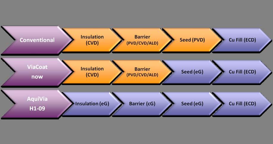
2 Overview Introduction Electrografting (eg) Technology Description Application to TSVs eg technical Characterization Resistivity Uniformity Step coverage Adhesion Electrografting Process Roadmap Fully Grafted Stack Step coverage Uniformity Adhesion Conclusion
3 Company Overview Started in 2001 as a spin off from the CEA, the French atomic energy authority Alchimer has developed materials and process IP for creating thin coatings on the inside of high-aspect ratio Through-Silicon Vias (TSVs) 22 patents families granted or filed Investors include Auriga Partners, AGF Private Equity, CEA Valorisation, Rothschild, Partech Partners, Intel Capital and Seventure Laboratory and offices located in Massy, near Paris, France Team of high level scientists in the fields of surface science, chemistry, electrochemistry, physics, materials science and semiconductors As an IP company, Alchimer s business model is based on licensing the technology to the users, as well as those providing production volumes of chemistry Page 3

4 Wet Chemical Nanofilm Technology Chemical functionalization of conducting and semi-conducting surfaces Proprietary wet technologies electrografting eg TM chemical grafting cg TM Permits the application of highly controlled, ultrathin coatings providing three key properties: Conformality Uniformity and Adhesion Enables economical TSVs with aspect ratios of 10:1 +


5 What is Electrografting? A breakthrough electrochemical process for creating nanoscale films on conductors and semiconductors Substrate is exposed to organic precursors Electrons from the biased surface serve as bonding seeds for precursor molecules This initiates the growth of a film that is grafted to the surface with co-valent bonds Provides nanometer thickness control from 5 to 500nm extended to 3000nm

6 Electro-initiated reactions yield conformality electro-deposition: F α grad(v) electro-grafting: F α grad(c) isopotential line isoconcentration line uniform density of electro-grafted precursors & purely chemical chain growth ultra-conformal electro-grafted layers

7 3-D IC barriers to adoption technological roadblocks TSV filling COST 30% + OF COST IS IN VIA ISOLATION/BARRIER/SEED/FIL L ipvd electro grafting Equipmen t Cost 6 MUS$ 2MUS$ 32% Source: Yole Developpement
8 Current TSV Process Challenges Via etch Bosch process scalloping Insulation deposition Organic: non integrated process step Barrier and Cu seed deposition High Aspect Ratio TSVs Sidewall coverage 0verburden Frequent adjustments to process parameters for different structures Via Fill by Electroplating voids if Cu seed is discontinuous 5:1 Via


9 TSV process flow with electrografting Via etch Films are very conformal to scalloped walls Insulation deposition Uniform growth of organic layer, integrated with subsequent steps Barrier and Cu seed deposition Excellent step coverage and adhesion in High Aspect Ratio TSVs Excellent Sidewall coverage No 0verburden Process parameters independent from via structures Via Fill by Electroplating No voids caused by discontinuities discontinuous barrier/adhesion layer Continuous, conformal electrografted film TiN barrier deposited by ASM Photos courtesy of NEXX

10 Electrografting Cu Seed performance Enables void free
11 Electrografted copper resistivity resistivity vs. eg layer thickness 1.8 Confidential Alchimer s.a.


12 Step Coverage on 5*50µm TSVs Dense Via : step coverage 90% TiN barrier deposited by ASM eg ViaCoat 98nm eg ViaCoat 109nm eg ViaCoat 129nm
 35 30 25")
 adhesion failure at ECP Cu /")

13 Adhesion of Electrografting Layers Adhesion Energy Gc (J/m²) Disp. (mm) adhesion failure at ECP Cu / glue interface eg Seed + ECP 4PB measurement Confidential Alchimer s.a.
14 Infrastructural Compatibility of Electrografting Fully compatible with electrochemical deposition of copper seed layers for the metallization of Thru Silicon Vias ready-to-use, mildly acidic, ultra-pure aqueous copperbased electrolyte solution compatible with industry-standard copper electroplating equipment and CMP processing compatible with standard blend waste stream and on-line monitoring systems
15 Electrografting Process Roadmap
16 Full Wet stack on 5 x 25 µm vias AquiVia
17 Initial characterization on 200-mm wafers eg ViaCoat Barrier Insulation eg insulator Thickness: 36 to 53nm Uniformity: 9% Adhesion: Passes scribe 16/16 squares tests without anneal up to 0.6µm thick Step Coverage: Insulator : 70% Barrier : 80% Cu : 66% eg Isolation Parameter MRS obj. Unit Thickness 400 nm Resistivity 5E14 µohm.cm Step coverage % Via diameter µm Aspect ratio >10 :1 Refraction index 1,5 / Dielectric constant / Dielectric strength 3.6E6 V/cm eg Barrier Parameter MRS obj. Unit Thickness nm nm Resistivity 25 µohm.cm Step coverage % Via diameter µm Aspect ratio >10 :1
18 Cost of Ownership per Wafer - Comparison Table ViaCoat Description Dry Process Grafting Process Benefit AquiVia Description Dry Process Grafting Process Benefit Equipment $10.0 $2.0 80% Consumables $15.0 $3.0 80% Labor $2.3 $0.5 78% Clean Room $0.9 $0.4 56% Overhead $2.8 $0.6 79% Total $31.0 $6.5 79% Equipment $33 $19 42% Consumables $36 $12 67% Labor $8 $6 25% Clean Room $4 $2 50% Overhead $8 $4 52% Total $89 $43 52% Assumptions: Wafers: 50K 300mm wafer starts per month; 95% process yield; TSVs: 5μm diameter, 50μm deep TSVs Clean Room: Cost = 250US$/sqft; Equipment footprint ratio = 2.5 (Source: Sematech) Dry Process Seed Deposition: - CoC for 10:1 AR TSV Wafer is 10X that of 1:1 AR Dual Damascene - Throughput for 10:1 AR TSV Wafer is 20% that of 1:1 AR Dual Damascene (Internal Source) Notes: 1) Dry Process - Number of Tools: - PECVD: 3 - i-pvd: 10 - ECD: 8 E3 Process Number of Tools: - ECD-eG: 8 - ECD-Fill: 7 2) 1 operator every 2 machines; 1 technician every 4 machines; 5 shifts 3) Includes equipment, facilities, operating costs

19 Conclusion Electrografting and chemical grafting approach to TSV layer deposition solves all current TSV technical challenges for isolation, barrier and seed ViaCoat TSV seed is a low cost high performance solution to a wide range of via dimensions exceeding 10:1 A/R AquiVia breaks down cost barriers preventing large scale adoption of 3D-IC applications For further information and reader enquiries: Emmanuel Guidotti Tel: emmanuel.guidotti@alchimer.com Fax: Web:
Electrografted insulator layer as copper diffusion barrier for TSV interposers
 Electrografted insulator layer as copper diffusion barrier for TSV interposers V. Mevellec, D. Suhr, T. Dequivre, P. Blondeau, L. Religieux and F. Raynal Scottsdale/Fountain Hills March 12-14, 2013 3D
Alternative deposition solution for cost reduction of TSV integration
 Alternative deposition solution for cost reduction of TSV integration J. Vitiello, F. Piallat, L. Bonnet KOBUS 611 rue Aristide Bergès, Z.A. de Pré Millet, Montbonnot-Saint-Martin, 38330 France Ph: +33
Thin Wafer Handling Debonding Mechanisms
 Thin Wafer Handling Debonding Mechanisms Jonathan Jeauneau, Applications Manager Alvin Lee, Technology Strategist Dongshun Bai, Scientist, 3-D IC R&D Materials Outline Requirements of Thin Wafer Handling
Passionately Innovating With Customers To Create A Connected World
 Passionately Innovating With Customers To Create A Connected World Multi Die Integration Can Material Suppliers Meet the Challenge? Nov 14, 2012 Jeff Calvert - R&D Director, Advanced Packaging Technologies
Hybrid Wafer Level Bonding for 3D IC
 Hybrid Wafer Level Bonding for 3D IC An Equipment Perspective Markus Wimplinger, Corporate Technology Development & IP Director History & Roadmap - BSI CIS Devices???? 2013 2 nd Generation 3D BSI CIS with
EV Group. Enabling processes for 3D interposer. Dr. Thorsten Matthias EV Group
 EV Group Enabling processes for 3D interposer Dr. Thorsten Matthias EV Group EV Group in a Nutshell st Our philosophy Our mission in serving next generation application in semiconductor technology Equipment
Film Deposition Part 1
 1 Film Deposition Part 1 Chapter 11 : Semiconductor Manufacturing Technology by M. Quirk & J. Serda Spring Semester 2013 Saroj Kumar Patra Semidonductor Manufacturing Technology, Norwegian University of
A Temporary Bonding and Debonding Technology for TSV Fabrication
 A Temporary Bonding and Debonding Technology for TSV Fabrication Taku Kawauchi, Masatoshi Shiraishi, Satoshi Okawa, Masahiro Yamamoto Tokyo Electron Ltd, Japan Taku Kawauchi, Tokyo Electron Ltd./Slide
Thin Wafer Handling Challenges and Emerging Solutions
 1 Thin Wafer Handling Challenges and Emerging Solutions Dr. Shari Farrens, Mr. Pete Bisson, Mr. Sumant Sood and Mr. James Hermanowski SUSS MicroTec, 228 Suss Drive, Waterbury Center, VT 05655, USA 2 Thin
MICROCHIP MANUFACTURING by S. Wolf
 by S. Wolf Chapter 15 ALUMINUM THIN-FILMS and SPUTTER-DEPOSITION 2004 by LATTICE PRESS CHAPTER 15 - CONTENTS Aluminum Thin-Films Sputter-Deposition Process Steps Physics of Sputter-Deposition Magnetron-Sputtering
LATEST INSIGHTS IN MATERIAL AND PROCESS TECHNOLOGIES FOR INTERPOSER AND 3D STACKING
 LATEST INSIGHTS IN MATERIAL AND PROCESS TECHNOLOGIES FOR INTERPOSER AND 3D STACKING European 3D TSV Summit, January 22-23, 2013, Grenoble Dr. Rainer Knippelmeyer, CTO and VP of R&D, GM Product Line Bonder
Model 2300XP PSL & Process-Particle Wafer Deposition System
 Model 2300XP PSL & Process-Particle Wafer Deposition System Deposit PSL spheres on wafers to create NISTtraceable PSL size standards for - calibrating wafer inspection systems - providing fab-wide and
Update in Material and Process Technologies for 2.5/3D IC Dr. Rainer Knippelmeyer CTO and VP R&D, SÜSS MicroTec AG
 Update in Material and Process Technologies for 2.5/3D IC Dr. Rainer Knippelmeyer CTO and VP R&D, SÜSS MicroTec AG TEMPORARY BONDING / DEBONDING AS THIN WAFER HANDLING SOLUTION FOR 3DIC & INTERPOSERS Device
CVD: General considerations.
 CVD: General considerations. PVD: Move material from bulk to thin film form. Limited primarily to metals or simple materials. Limited by thermal stability/vapor pressure considerations. Typically requires
Solliance. Perovskite based PV (PSC) Program. TKI Urban Energy Days l e d b y i m e c, E C N a n d T N O
 Program. TKI Urban Energy Days l e d b y i m e c, E C N a n d T N O") Solliance Perovskite based PV (PSC) Program TKI Urban Energy Days - 2017-06-21 l e d b y i m e c, E C N a n d T N O 2 Bringing together research and industry Providing insight and know-how to all partners
Solliance Perovskite based PV (PSC) Program TKI Urban Energy Days - 2017-06-21 l e d b y i m e c, E C N a n d T N O 2 Bringing together research and industry Providing insight and know-how to all partners
Lecture 8. Photoresists and Non-optical Lithography
 Lecture 8 Photoresists and Non-optical Lithography Reading: Chapters 8 and 9 and notes derived from a HIGHLY recommended book by Chris Mack, Fundamental Principles of Optical Lithography. Any serious student
Fabrication Technology, Part I
 EEL5225: Principles of MEMS Transducers (Fall 2004) Fabrication Technology, Part I Agenda: Microfabrication Overview Basic semiconductor devices Materials Key processes Oxidation Thin-film Deposition Reading:
Structuring and bonding of glass-wafers. Dr. Anke Sanz-Velasco
 Structuring and bonding of glass-wafers Dr. Anke Sanz-Velasco Outline IMT Why glass? Components for life science Good bond requirements and evaluation Wafer bonding 1. Fusion bonding 2. UV-adhesive bonding
UNIVERSITY OF CALIFORNIA College of Engineering Department of Electrical Engineering and Computer Sciences. Fall Exam 1
 UNIVERSITY OF CALIFORNIA College of Engineering Department of Electrical Engineering and Computer Sciences EECS 143 Fall 2008 Exam 1 Professor Ali Javey Answer Key Name: SID: 1337 Closed book. One sheet
The goal of this project is to enhance the power density and lowtemperature efficiency of solid oxide fuel cells (SOFC) manufactured by atomic layer
 manufactured by atomic layer") Stanford University Michael Shandalov1, Shriram Ramanathan2, Changhyun Ko2 and Paul McIntyre1 1Department of Materials Science and Engineering, Stanford University 2Division of Engineering and Applied
Stanford University Michael Shandalov1, Shriram Ramanathan2, Changhyun Ko2 and Paul McIntyre1 1Department of Materials Science and Engineering, Stanford University 2Division of Engineering and Applied
UHF-ECR Plasma Etching System for Dielectric Films of Next-generation Semiconductor Devices
 UHF-ECR Plasma Etching System for Dielectric Films of Next-generation Semiconductor Devices 1 UHF-ECR Plasma Etching System for Dielectric Films of Next-generation Semiconductor Devices Katsuya Watanabe
Case Study of Electronic Materials Packaging with Poor Metal Adhesion and the Process for Performing Root Cause Failure Analysis
 Case Study of Electronic Materials Packaging with Poor Metal Adhesion and the Process for Performing Root Cause Failure Analysis Dr. E. A. Leone BACKGRUND ne trend in the electronic packaging industry
XBC300 Gen2. Fully-automated debonder and Cleaner
 XBC300 Gen2 Fully-automated debonder and Cleaner XBC300 Gen2 FULLY AUTOMATED DEBONDER AND CLEANER The SUSS XBC300 Gen2 debonder and cleaner platform is designed for process development as well as high
Temporary Wafer Bonding - Key Technology for 3D-MEMS Integration
 Temporary Wafer Bonding - Key Technology for 3D-MEMS Integration 2016-06-15, Chemnitz Chemnitz University of Technology Basic Research Fraunhofer ENAS System-Packaging (SP) Back-End of Line (BEOL) Applied
Chapter 3 Basics Semiconductor Devices and Processing
 Chapter 3 Basics Semiconductor Devices and Processing Hong Xiao, Ph. D. www2.austin.cc.tx.us/hongxiao/book.htm Hong Xiao, Ph. D. www2.austin.cc.tx.us/hongxiao/book.htm 1 Objectives Identify at least two
Superconducting Ti/TiN thin films for mm wave absorption
 Superconducting /N thin films for mm wave absorption A.Aliane 1, M. Solana 2, V. Goudon 1, C. Vialle 1, S. Pocas 1, E. Baghe 1, L. Carle 1, W. Rabaud 1, L. Saminadayar 2, L. Dussopt 1, P.Agnese 1, N. Lio
Superconducting Through-Silicon Vias for Quantum Integrated Circuits
 Superconducting Through-Silicon Vias for Quantum Integrated Circuits Mehrnoosh Vahidpour, William O Brien, Jon Tyler Whyland, Joel Angeles, Jayss Marshall, Diego Scarabelli, Genya Crossman, Kamal Yadav,
Introduction to Photolithography
 http://www.ichaus.de/news/72 Introduction to Photolithography Photolithography The following slides present an outline of the process by which integrated circuits are made, of which photolithography is
EV Group. Engineered Substrates for future compound semiconductor devices
 EV Group Engineered Substrates for future compound semiconductor devices Engineered Substrates HB-LED: Engineered growth substrates GaN / GaP layer transfer Mobility enhancement solutions: III-Vs to silicon
Self-study problems and questions Processing and Device Technology, FFF110/FYSD13
 Self-study problems and questions Processing and Device Technology, FFF110/FYSD13 Version 2016_01 In addition to the problems discussed at the seminars and at the lectures, you can use this set of problems
OPTIMIZATION OF DIELECTRICS SURFACE PREPARATION FOR VACUUM COATING
 OPTIMIZATION OF DIELECTRICS SURFACE PREPARATION FOR VACUUM COATING Dr. Boris Statnikov Introduction Modern MICRO and NANO technologies in ultra- and high-frequency electronics are widely focused on application
Regents of the University of California
 Deep Reactive-Ion Etching (DRIE) DRIE Issues: Etch Rate Variance The Bosch process: Inductively-coupled plasma Etch Rate: 1.5-4 μm/min Two main cycles in the etch: Etch cycle (5-15 s): SF 6 (SF x+ ) etches
TCAD Modeling of Stress Impact on Performance and Reliability
 TCAD Modeling of Stress Impact on Performance and Reliability Xiaopeng Xu TCAD R&D, Synopsys March 16, 2010 SEMATECH Workshop on Stress Management for 3D ICs using Through Silicon Vias 1 Outline Introduction
EE 527 MICROFABRICATION. Lecture 25 Tai-Chang Chen University of Washington
 EE 527 MICROFABRICATION Lecture 25 Tai-Chang Chen University of Washington ION MILLING SYSTEM Kaufmann source Use e-beam to strike plasma A magnetic field applied to increase ion density Drawback Low etch
Plasma Deposition (Overview) Lecture 1
 Lecture 1") Plasma Deposition (Overview) Lecture 1 Material Processes Plasma Processing Plasma-assisted Deposition Implantation Surface Modification Development of Plasma-based processing Microelectronics needs (fabrication
Plasma Deposition (Overview) Lecture 1 Material Processes Plasma Processing Plasma-assisted Deposition Implantation Surface Modification Development of Plasma-based processing Microelectronics needs (fabrication
Developer-soluble Gap fill materials for patterning metal trenches in Via-first Dual Damascene process
 Developer-soluble Gap fill materials for patterning metal trenches in Via-first Dual Damascene process Mandar Bhave, Kevin Edwards, Carlton Washburn Brewer Science, Inc., 2401 Brewer Dr., Rolla, MO 65401,
VACUUM TECHNOLOGIES NEEDED FOR 3D DEVICE PROCESSING
 VACUUM TECHNOLOGIES NEEDED FOR 3D DEVICE PROCESSING Future ICs will use more 3D device structures such as finfets and gate-all-around (GAA) transistors, and so vacuum deposition processes are needed that
A Mechanical Model for Erosion in Copper Chemical-Mechanical Polishing
 A Mechanical Model for Erosion in Copper Chemical-Mechanical Polishing Kyungyoon Noh, Nannaji Saka and Jung-Hoon Chun Laboratory for Manufacturing and Productivity Massachusetts Institute of Technology
A New High Voltage 4H-SiC Lateral Dual Sidewall Schottky (LDSS) Rectifier: Theoretical Investigation and Analysis
 Rectifier: Theoretical Investigation and Analysis") M. Jagadesh Kumar and C. Linga Reddy, "A New High Voltage 4H-SiC Lateral Dual Sidewall Schottky (LDSS) Rectifier: Theoretical Investigation and Analysis", IEEE Trans. on Electron Devices, Vol.50, pp.1690-1693,
M. Jagadesh Kumar and C. Linga Reddy, "A New High Voltage 4H-SiC Lateral Dual Sidewall Schottky (LDSS) Rectifier: Theoretical Investigation and Analysis", IEEE Trans. on Electron Devices, Vol.50, pp.1690-1693,
Three Approaches for Nanopatterning
 Three Approaches for Nanopatterning Lithography allows the design of arbitrary pattern geometry but maybe high cost and low throughput Self-Assembly offers high throughput and low cost but limited selections
SCI. Scientific Computing International. Scientific Computing International. FilmTek. Raising Thin Film Metrology Performance to a New Level
 FilmTek Raising Thin Film Metrology Performance to a New Level 1 Through Silicon Via (TSV) Metrology FilmTek TM TM TSV TSV Metrology Advantages Measure high aspect ratio TSV structures (up to 30:1) Measure
Yield. Economics. Victor Ovchinnikov. Chapters 36, 37
 Yield. Economics Victor Ovchinnikov Chapters 36, 37 Previous material CMOS Released structural layers MEMS Multilayer metallization Aalto Nanofab, 2017 Microfabrication 2 Content Yield definition Yield
Carbon Nanotubes for Interconnect Applications Franz Kreupl, Andrew P. Graham, Maik Liebau, Georg S. Duesberg, Robert Seidel, Eugen Unger
 Carbon Nanotubes for Interconnect Applications Franz Kreupl, Andrew P. Graham, Maik Liebau, Georg S. Duesberg, Robert Seidel, Eugen Unger Infineon Technologies Corporate Research Munich, Germany Outline
LECTURE 5 SUMMARY OF KEY IDEAS
 LECTURE 5 SUMMARY OF KEY IDEAS Etching is a processing step following lithography: it transfers a circuit image from the photoresist to materials form which devices are made or to hard masking or sacrificial
Taurus-Topography. Topography Modeling for IC Technology
 SYSTEMS PRODUCTS LOGICAL PRODUCTS PHYSICAL IMPLEMENTATION SIMULATION AND ANALYSIS LIBRARIES TCAD Aurora DFM WorkBench Davinci Medici Raphael Raphael-NES Silicon Early Access TSUPREM-4 Taurus-Device Taurus-Lithography
From Hall Effect to TMR
 From Hall Effect to TMR 1 Abstract This paper compares the century old Hall effect technology to xmr technologies, specifically TMR (Tunnel Magneto-Resistance) from Crocus Technology. It covers the various
Sensors and Metrology. Outline
 Sensors and Metrology A Survey 1 Outline General Issues & the SIA Roadmap Post-Process Sensing (SEM/AFM, placement) In-Process (or potential in-process) Sensors temperature (pyrometry, thermocouples, acoustic
Chapter 10 3D Integration Based upon Dielectric Adhesive Bonding
 Chapter 10 3D Integration Based upon Dielectric Adhesive Bonding Jian-Qiang Lu, Timothy S. Cale, and Ronald J. Gutmann 10.1 Introduction Wafer bonding with intermediate polymer adhesives is one of the
EE C245 ME C218 Introduction to MEMS Design Fall 2007
 EE C245 ME C218 Introduction to MEMS Design Fall 2007 Prof. Clark T.-C. Nguyen Dept. of Electrical Engineering & Computer Sciences University of California at Berkeley Berkeley, CA 94720 Lecture 12: Mechanics
nmos IC Design Report Module: EEE 112
 nmos IC Design Report Author: 1302509 Zhao Ruimin Module: EEE 112 Lecturer: Date: Dr.Zhao Ce Zhou June/5/2015 Abstract This lab intended to train the experimental skills of the layout designing of the
Lecture 0: Introduction
 Lecture 0: Introduction Introduction q Integrated circuits: many transistors on one chip q Very Large Scale Integration (VLSI): bucketloads! q Complementary Metal Oxide Semiconductor Fast, cheap, low power
Nanoscale IR spectroscopy of organic contaminants
 The nanoscale spectroscopy company The world leader in nanoscale IR spectroscopy Nanoscale IR spectroscopy of organic contaminants Application note nanoir uniquely and unambiguously identifies organic
Thermo-structural Model of Stacked Field-programmable Gate Arrays (FPGAs) with Through-silicon Vias (TSVs)
 with Through-silicon Vias (TSVs)") Manuscript for Review Thermo-structural Model of Stacked Field-programmable Gate Arrays (FPGAs) with Through-silicon Vias (TSVs) Journal: Electronics Letters Manuscript ID: draft Manuscript Type: Letter
Manuscript for Review Thermo-structural Model of Stacked Field-programmable Gate Arrays (FPGAs) with Through-silicon Vias (TSVs) Journal: Electronics Letters Manuscript ID: draft Manuscript Type: Letter
SUPPLEMENTARY NOTES Supplementary Note 1: Fabrication of Scanning Thermal Microscopy Probes
 SUPPLEMENTARY NOTES Supplementary Note 1: Fabrication of Scanning Thermal Microscopy Probes Fabrication of the scanning thermal microscopy (SThM) probes is summarized in Supplementary Fig. 1 and proceeds
True Room Temperature Bonding a novel process for the creation of health tech consumables ATB. ir. Richard Bijlard Technogation - Invenios
 True Room Temperature Bonding a novel process for the creation of health tech consumables ATB ir. Richard Bijlard Technogation - Invenios Technogation Invenios Dec 2014 Presentation Overview Invenios Group
Solutions for Assignment-6
 Solutions for Assignment-6 Q1. What is the aim of thin film deposition? [1] (a) To maintain surface uniformity (b) To reduce the amount (or mass) of light absorbing materials (c) To decrease the weight
A STUDY OF ATOMIC LAYER DEPOSITION AND REACTIVE PLASMA COMPATIBILITY WITH MESOPOROUS ORGANOSILICATE GLASS FILMS
 A STUDY OF ATOMIC LAYER DEPOSITION AND REACTIVE PLASMA COMPATIBILITY ITH MESOPOROUS ORGANOSILICATE GLASS FILMS E. Todd Ryan*, Melissa Freeman, Lynne Svedberg, J.J. Lee, Todd Guenther, Jim Connor, Katie
Chapter 7 Plasma Basic
 Chapter 7 Plasma Basic Hong Xiao, Ph. D. hxiao89@hotmail.com www2.austin.cc.tx.us/hongxiao/book.htm Hong Xiao, Ph. D. www2.austin.cc.tx.us/hongxiao/book.htm 1 Objectives List at least three IC processes
Multi Beam Sputtering
 Equipment Manufacturer Multi Beam Sputtering Customization of ion beam deposition Our activities Compact ECR Ion sources Custom ion beam systems (ion implanter) Thin film deposition «on-demand» Thin film
Characterization of Post-etch Residue Clean By Chemical Bonding Transformation Mapping
 Characterization of Post-etch Residue Clean By Chemical Bonding Transformation Mapping Muthappan Asokan, Oliver Chyan*, Interfacial Electrochemistry and Materials Research Lab, University of North Texas
Advances in Back-side Via Etching of SiC for GaN Device Applications
 Advances in Back-side Via Etching of SiC for GaN Device Applications Anthony Barker, Kevin Riddell, Huma Ashraf & Dave Thomas SPTS Technologies, Ringland Way, Newport NP18 2TA, UK, dave.thomas@spts.com,
TECHCET s Review of Sematech s Surface Preparation & Cleaning Conference Saratoga Springs, NY, May 12-14, 2015 Part 1 of 2
 TECHCET s Review of Sematech s Surface Preparation & Cleaning Conference Saratoga Springs, NY, May 12-14, 2015 Part 1 of 2 Presentations from SPCC related to the latest Wet Cleaning / Etching / Surface
MaxCaps Next Generation Dielectrics for Integrated Capacitors
 MaxCaps Next Generation Dielectrics for Integrated Capacitors Guenther Ruhl Infineon Technologies AG Σ! 2365 Semicon Europa 2011 Dresden, October 11, 2011 October 11, 2011 1 Outline Introduction MaxCaps
ECE520 VLSI Design. Lecture 8: Interconnect Manufacturing and Modeling. Payman Zarkesh-Ha
 ECE520 VLSI Design Lecture 8: Interconnect Manufacturing and Modeling Payman Zarkesh-Ha Office: ECE Bldg. 230B Office hours: Wednesday 2:00-3:00PM or by appointment E-mail: pzarkesh@unm.edu Slide: 1 Review
SHRINK. STACK. INTEGRATE.
 SHRINK. STACK. INTEGRATE. SUSS MICROTEC PRODUCT PORTFOLIO SHAPING THE FUTURE With more than 60 years of engineering experience SUSS MicroTec is a leading supplier of process equipment for microstructuring
Südliche Stadtmauerstr. 15a Tel: D Erlangen Fax:
 Curriculum Vitae Lionel Santinacci 19.10.1974 Nationality: French Südliche Stadtmauerstr. 15a Tel: + 49 9131 852 7587 D-91054 Erlangen Fax: + 49 9131 852 7582 Germany e-mail: lionel@ww.uni-erlangen.de
Multilayer Wiring Technology with Grinding Planarization of Dielectric Layer and Via Posts
 Tani et al.: Multilayer Wiring Technology with Grinding Planarization (1/6) [Technical Paper] Multilayer Wiring Technology with Grinding Planarization of Dielectric Layer and Via Posts Motoaki Tani, Kanae
Competitive Advantages of Ontos7 Atmospheric Plasma
 Competitive Advantages of Ontos7 Atmospheric Plasma Eric Schulte Matt Phillips Keith Cooper SETNA Proprietary 1 Advantages of Ontos7 Atmospheric Plasma Process over Vacuum RIE Plasma for Die/Wafer Surface
UNIVERSITY OF CALIFORNIA. College of Engineering. Department of Electrical Engineering and Computer Sciences. Professor Ali Javey.
 UNIVERSITY OF CALIFORNIA College of Engineering Department of Electrical Engineering and Computer Sciences EE 143 Professor Ali Javey Spring 2009 Exam 2 Name: SID: Closed book. One sheet of notes is allowed.
Available online at ScienceDirect. Procedia Engineering 152 (2016 )
") Available online at www.sciencedirect.com ScienceDirect Procedia Engineering 152 (2016 ) 706 710 International Conference on Oil and Gas Engineering, OGE-2016 Synthesis of the carbon nanotubes-porous silicon
Available online at www.sciencedirect.com ScienceDirect Procedia Engineering 152 (2016 ) 706 710 International Conference on Oil and Gas Engineering, OGE-2016 Synthesis of the carbon nanotubes-porous silicon
Wet Clean Challenges for Various Applications
 Wet Clean Challenges for Various Applications Business of Cleans Conference 2018 Stephen Olson, Martin Rodgers, Satyavolu Papa Rao, Chris Borst solson@sunypoly.edu Outline SUNY Poly Introduction Background
Chapter 3 Engineering Science for Microsystems Design and Fabrication
 Lectures on MEMS and MICROSYSTEMS DESIGN and MANUFACTURE Chapter 3 Engineering Science for Microsystems Design and Fabrication In this Chapter, we will present overviews of the principles of physical and
Nanostructure. Materials Growth Characterization Fabrication. More see Waser, chapter 2
 Nanostructure Materials Growth Characterization Fabrication More see Waser, chapter 2 Materials growth - deposition deposition gas solid Physical Vapor Deposition Chemical Vapor Deposition Physical Vapor
EE130: Integrated Circuit Devices
 EE130: Integrated Circuit Devices (online at http://webcast.berkeley.edu) Instructor: Prof. Tsu-Jae King (tking@eecs.berkeley.edu) TA s: Marie Eyoum (meyoum@eecs.berkeley.edu) Alvaro Padilla (apadilla@eecs.berkeley.edu)
F R A U N H O F E R I N
 FRAUNHOFER Institute FoR Electronic NAno systems ENAS System Packaging 1 2 3 4 5 The actual developments of micro and nano technologies are fascinating. Undoubted they are playing a key role in today s
Research and Development of Parylene Thin-Film Deposition and Application for Water-Proofing
 Advanced Materials Research Online: 2012-06-14 ISSN: 1662-8985, Vols. 538-541, pp 23-28 doi:10.4028/www.scientific.net/amr.538-541.23 2012 Trans Tech Publications, Switzerland Research and Development
EE C245 ME C218 Introduction to MEMS Design Fall 2007
 EE C245 ME C218 Introduction to MEMS Design Fall 2007 Prof. Clark T.-C. Nguyen Dept. of Electrical Engineering & Computer Sciences University of California at Berkeley Berkeley, CA 94720 Lecture 4: Film
Reliability of 3D IC with Via-Middle TSV: Characterization and Modeling
 Reliability of 3D IC with Via-Middle TSV: Characterization and Modeling Victor Moroz *, Munkang Choi *, Geert Van der Plas, Paul Marchal, Kristof Croes, and Eric Beyne * Motivation: Build Reliable 3D IC
Nanostrukturphysik (Nanostructure Physics)
") Nanostrukturphysik (Nanostructure Physics) Prof. Yong Lei & Dr. Yang Xu Fachgebiet 3D-Nanostrukturierung, Institut für Physik Contact: yong.lei@tu-ilmenau.de; yang.xu@tu-ilmenau.de Office: Unterpoerlitzer
Nanostrukturphysik (Nanostructure Physics) Prof. Yong Lei & Dr. Yang Xu Fachgebiet 3D-Nanostrukturierung, Institut für Physik Contact: yong.lei@tu-ilmenau.de; yang.xu@tu-ilmenau.de Office: Unterpoerlitzer
Wet Chemical Processing with Megasonics Assist for the Removal of Bumping Process Photomasks
 Wet Chemical Processing with Megasonics Assist for the Removal of Bumping Process Photomasks Hongseong Sohn and John Tracy Akrion Systems 6330 Hedgewood Drive, Suite 150 Allentown, PA 18106, USA Abstract
THIN-FILM MEASUREMENT
 ADVANCED THIN-FILM MEASUREMENT SYSTEMS TAKING THE MYSTERY OUT OF THIN-FILM MEASUREMENT ABOUT THIN-FILM MEASUREMENTS THIN-FILM MEASUREMENT Introduction Thin film Thin films are very thin layers of material
Solutions for Assignment-8
 Solutions for Assignment-8 Q1. The process of adding impurities to a pure semiconductor is called: [1] (a) Mixing (b) Doping (c) Diffusing (d) None of the above In semiconductor production, doping intentionally
DEPOSITION OF THIN TiO 2 FILMS BY DC MAGNETRON SPUTTERING METHOD
 Chapter 4 DEPOSITION OF THIN TiO 2 FILMS BY DC MAGNETRON SPUTTERING METHOD 4.1 INTRODUCTION Sputter deposition process is another old technique being used in modern semiconductor industries. Sputtering
E SC 412 Nanotechnology: Materials, Infrastructure, and Safety Wook Jun Nam
 E SC 412 Nanotechnology: Materials, Infrastructure, and Safety Wook Jun Nam Lecture 10 Outline 1. Wet Etching/Vapor Phase Etching 2. Dry Etching DC/RF Plasma Plasma Reactors Materials/Gases Etching Parameters
EE C245 ME C218 Introduction to MEMS Design Fall 2007
 EE C245 ME C218 Introduction to MEMS Design Fall 2007 Prof. Clark T.-C. Nguyen Dept. of Electrical Engineering & Computer Sciences University of California at Berkeley Berkeley, CA 94720 Lecture 11: Bulk
Molecular Electronics For Fun and Profit(?)
") Molecular Electronics For Fun and Profit(?) Prof. Geoffrey Hutchison Department of Chemistry University of Pittsburgh geoffh@pitt.edu July 22, 2009 http://hutchison.chem.pitt.edu Moore s Law: Transistor
Molecular Electronics For Fun and Profit(?) Prof. Geoffrey Hutchison Department of Chemistry University of Pittsburgh geoffh@pitt.edu July 22, 2009 http://hutchison.chem.pitt.edu Moore s Law: Transistor
Top down and bottom up fabrication
 Lecture 24 Top down and bottom up fabrication Lithography ( lithos stone / graphein to write) City of words lithograph h (Vito Acconci, 1999) 1930 s lithography press Photolithography d 2( NA) NA=numerical
Thin Film Deposition. Reading Assignments: Plummer, Chap 9.1~9.4
 Thin Film Deposition Reading Assignments: Plummer, Chap 9.1~9.4 Thermally grown Deposition Thin Film Formation Thermally grown SiO 2 Deposition SiO 2 Oxygen is from gas phase Silicon from substrate Oxide
ORION NanoFab: An Overview of Applications. White Paper
 ORION NanoFab: An Overview of Applications White Paper ORION NanoFab: An Overview of Applications Author: Dr. Bipin Singh Carl Zeiss NTS, LLC, USA Date: September 2012 Introduction With the advancement
(12) Patent Application Publication (10) Pub. No.: US 2014/ A1
 Patent Application Publication (10) Pub. No.: US 2014/ A1") (19) United States US 20140238873A1 (12) Patent Application Publication (10) Pub. No.: US 2014/0238873 A1 Li et al. (43) Pub. Date: Aug. 28, 2014 (54) MODIFIED BUBBLING TRANSFER METHOD (52) U.S. Cl. FOR
(19) United States US 20140238873A1 (12) Patent Application Publication (10) Pub. No.: US 2014/0238873 A1 Li et al. (43) Pub. Date: Aug. 28, 2014 (54) MODIFIED BUBBLING TRANSFER METHOD (52) U.S. Cl. FOR
Hotwire-assisted Atomic Layer Deposition of Pure Metals and Metal Nitrides
 Hotwire-assisted Atomic Layer Deposition of Pure Metals and Metal Nitrides Alexey Kovalgin MESA+ Institute for Nanotechnology Semiconductor Components group a.y.kovalgin@utwente.nl 1 Motivation 1. Materials
EN2912C: Future Directions in Computing Lecture 08: Overview of Near-Term Emerging Computing Technologies
 EN2912C: Future Directions in Computing Lecture 08: Overview of Near-Term Emerging Computing Technologies Prof. Sherief Reda Division of Engineering Brown University Fall 2008 1 Near-term emerging computing
Lecture 18: Microfluidic MEMS, Applications
 MECH 466 Microelectromechanical Systems University of Victoria Dept. of Mechanical Engineering Lecture 18: Microfluidic MEMS, Applications 1 Overview Microfluidic Electrokinetic Flow Basic Microfluidic
Datasheet Rev Flexible Printed Circuits For the latest information please visit
 Flame-resistant polyimide (PI) film based flexible copperclad laminates: base materials Specification Thickness [µm] Single/Double Copper PI-film Cu-foil dhesive sided type SF302 051813SR 13,0 18 13 single
Ag Seed-Layer Formation by Electroless Plating for Ultra-Large-Scale Integration Interconnection
 Downloaded 4 Jul to 147.46.246.152. Redistribution subject to ECS license or copyright; see http://www.ecsdl.org/terms_use.jsp D558 Journal of The Electrochemical Society, 155 9 D558-D562 8 13-4651/8/155
Developments in CMP and Impact on CMP Consumables
 Developments in CMP and Impact on CMP Consumables Mike Corbett Semicon West CMPUG July 12, 2017 mcorbett@linx-consulting.com Surface Preparation & Cleaning Conference External Disclosure Not Permitted
Scaling up Chemical Vapor Deposition Graphene to 300 mm Si substrates
 Scaling up Chemical Vapor Deposition Graphene to 300 mm Si substrates Co- Authors Aixtron Alex Jouvray Simon Buttress Gavin Dodge Ken Teo The work shown here has received partial funding from the European
Etching Issues - Anisotropy. Dry Etching. Dry Etching Overview. Etching Issues - Selectivity
 Etching Issues - Anisotropy Dry Etching Dr. Bruce K. Gale Fundamentals of Micromachining BIOEN 6421 EL EN 5221 and 6221 ME EN 5960 and 6960 Isotropic etchants etch at the same rate in every direction mask
Ph D in Physics from the University of Toulouse (UPS) and Post Graduate Diploma in research (HDR) from University of Grenoble (France).
 and Post Graduate Diploma in research (HDR) from University of Grenoble (France).") Aziz ZENASNI Ph D in Physics from the University of Toulouse (UPS) and Post Graduate Diploma in research (HDR) from University of Grenoble (France). Currently a Research Staff Member of CEA-LETI, he has
Aziz ZENASNI Ph D in Physics from the University of Toulouse (UPS) and Post Graduate Diploma in research (HDR) from University of Grenoble (France). Currently a Research Staff Member of CEA-LETI, he has
EE 292L : Nanomanufacturing. Week 5: Advanced Process Technology. Oct
 EE 292L : Nanomanufacturing Week 5: Advanced Process Technology Oct 22 2012 1 Advanced Process Technology 1 HAR etch 2 3 HAR Gapfill Metal ALD 4 Reflow 5 6 SAC Airgap 7 8 Strain Ge/III-V Engineering 1