Efficient electron transport on helium with silicon integrated circuits
|
|
|
- Shanon Boone
- 5 years ago
- Views:
Transcription


1 Efficient electron transport on helium with silicon integrated circuits Forrest Bradbury 1 and Maika Takita 1, Kevin Eng 2, Tom M Gurrieri 2, Kathy J Wilkel 2, Stephen A Lyon 1 1 Princeton University 2 Sandia National Laboratories

2 Electron spins on helium are low density, but independent, flexible, and mobile: the Quantum Information American Dream
3 Electron spins on helium are low density, but independent, flexible, and mobile: Stationary qubits necessitate continual SWAP operations on neighboring qubits for information propagation Mobile qubits obviate this extra requirement Mobile electron spins in silicon are so far the best, but their coherence is limited by the Rashba interaction to T 2 = 3 µs Electron spins on helium expected T 2 > 100 seconds
4 Transport enabled computation Memory registers... Interaction Post Dot Single charge detection
5 twiddle sense door 3um He 2um Twiddle Sensing SiO 2 3um ~ ~ 3 twiddle sense door Plate Plate HEMT Preamp at 1.5 K
6 twiddle sense door 3um He 2um Twiddle Sensing SiO 2 3um ~ ~ 3 twiddle sense door Plate Plate HEMT Preamp at 1.5 K

7 twiddle sense door 3um He 2um Twiddle Sensing SiO 2 3um ~ ~ 3 twiddle sense door Plate Plate HEMT Preamp at 1.5 K


8 Twiddle Sensor: Potential Simulations Top metal plane held at -3V Twiddling right: Φ3 Twiddle Sense Door Plate1-400mV -80mV 0mV -320mV -400mV Twiddling left: Φ3 Twiddle Sense Door Plate1-400mV +80mV 0mV -480mV -400mV Electrical potential in volts at the helium surface above the channels
9 Calibration Twiddle Sensing Results Voltage signal is converted to number of electrons per channel via gain calibration of the amplification circuit and capacitance estimate of the sense line + HEMT input. This predicts the observed signal saturation where detector is no longer linear. Linearity
10 Calibration Twiddle Sensing Results Voltage signal is converted to number of electrons per channel via gain calibration of the amplification circuit and capacitance estimate of the sense line + HEMT input. This predicts the observed signal saturation where detector is no longer linear. Linearity Twiddle Sensing Sensitivity Noise in silicon samples ~ 360 electrons per Hz ½ with 120 parallel channels ~ 3 electrons per channel per Hz ½
11 Twiddle Sensing Results Twiddle Sensing Sensitivity Noise in silicon samples Electrons per Channel Quantization Measurements ~ 360 electrons per Hz ½ with 120 parallel channels ~ 3 electrons per channel per Hz ½ Electron turnstile for confinement Lower temperature

12 Twiddle Sensing with On-chip Amplification Better sensing by proximity: With HEMT preamp, ~2 pf With on-chip FET, ~0.02 pf Induced voltage is 100x 13.5 µm
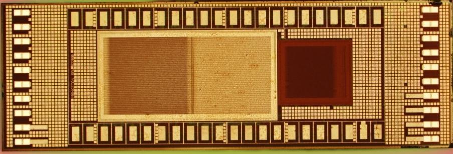

13 Multi-Project Wafer from Sandia CMOS7 Process
14 Potential Energy 3-phase CCD Potential Underlying gates Helium electron - +

15 Device structure 120 horizontal channels Measurement gates for electron detection Right and Left Memory Cell Gates Vccd2 Vccd3 twiddle sense door
16 Horizontal CCD Loading: Photoemit electrons on plates Load them to pixels by opening the door plate Clocking Sequence 10 pixel to the left 10 pixel back to the right door sense twiddle
17 # of electrons per channel Horizontal Clocking Efficiency Clock (pixel) rate = 240kHz pixels transferred No measurable loss after 10 9 cycles!
18 Vertical channel CCD Vertical Clocking Efficiency Cornering Efficiency Distribution of electrons in horizontal channels
19 Vertical channel CCD
20 Vertical channel CCD

21 Vertical channel CCD


22 Vertical channel CCD Distribution of electrons in horizontal channels
23 Vertical channel CCD Channel N+60 each packet of electrons travels up and down 60 channels C-cycling Demonstrates vertical channel CCD cornering efficiency 2D control Channel N
24 # of electrons per channel Vertical CCD Cornering 2D control Vertical channel CCD Channel 61 pixels transferred One packet of electrons travels between Channel occupancy after C-Cycle Channel 1 # of channels moved
25 Conclusion Electron detection with twiddle gate Unprecedented reliability of a Charge Coupled Device -Essentially a perfect Electron Transfer Efficiency 5 clock lines for full control -2D Scalability: Move anywhere in our ~5000 position gate & channel array Si-Processing -First, non-optimized design with standard silicon processing -Possibilities for on-chip amplification
Single Electron Transistor (SET)
") Single Electron Transistor (SET) SET: e - e - dot A single electron transistor is similar to a normal transistor (below), except 1) the channel is replaced by a small dot. C g 2) the dot is separated from
Single Electron Transistor (SET) SET: e - e - dot A single electron transistor is similar to a normal transistor (below), except 1) the channel is replaced by a small dot. C g 2) the dot is separated from
Fig. 1 CMOS Transistor Circuits (a) Inverter Out = NOT In, (b) NOR-gate C = NOT (A or B)
 Inverter Out = NOT In, (b) NOR-gate C = NOT (A or B)") 1 Introduction to Transistor-Level Logic Circuits 1 By Prawat Nagvajara At the transistor level of logic circuits, transistors operate as switches with the logic variables controlling the open or closed
1 Introduction to Transistor-Level Logic Circuits 1 By Prawat Nagvajara At the transistor level of logic circuits, transistors operate as switches with the logic variables controlling the open or closed
Developing Quantum Logic Gates: Spin-Resonance-Transistors
 Developing Quantum Logic Gates: Spin-Resonance-Transistors H. W. Jiang (UCLA) SRT: a Field Effect Transistor in which the channel resistance monitors electron spin resonance, and the resonance frequency
CIRCUIT QUANTUM ELECTRODYNAMICS WITH ELECTRONS ON HELIUM
 CIRCUIT QUANTUM ELECTRODYNAMICS WITH ELECTRONS ON HELIUM David Schuster Assistant Professor University of Chicago Chicago Ge Yang Bing Li Michael Geracie Yale Andreas Fragner Rob Schoelkopf Useful cryogenics
Lecture Notes 2 Charge-Coupled Devices (CCDs) Part I. Basic CCD Operation CCD Image Sensor Architectures Static and Dynamic Analysis
 Part I. Basic CCD Operation CCD Image Sensor Architectures Static and Dynamic Analysis") Lecture Notes 2 Charge-Coupled Devices (CCDs) Part I Basic CCD Operation CCD Image Sensor Architectures Static and Dynamic Analysis Charge Well Capacity Buried channel CCD Transfer Efficiency Readout Speed
Lecture Notes 2 Charge-Coupled Devices (CCDs) Part I Basic CCD Operation CCD Image Sensor Architectures Static and Dynamic Analysis Charge Well Capacity Buried channel CCD Transfer Efficiency Readout Speed
High Reliability Hallogic Hall- Effect Sensors OMH090, OMH3019, OMH3020, OMH3040, OMH3075, OMH3131 (B, S versions)
") High Reliability Hallogic Hall Features: Designed for noncontact switching operations Operates over a broad range of supply voltages Excellent temperature stability operates in harsh environments Suitable
High Reliability Hallogic Hall Features: Designed for noncontact switching operations Operates over a broad range of supply voltages Excellent temperature stability operates in harsh environments Suitable
Design Considerations for Integrated Semiconductor Control Electronics for a Large-scale Solid State Quantum Processor
 Design Considerations for Integrated Semiconductor Control Electronics for a Large-scale Solid State Quantum Processor Hendrik Bluhm Andre Kruth Lotte Geck Carsten Degenhardt 1 0 Ψ 1 Quantum Computing
single-electron electron tunneling (SET)
") single-electron electron tunneling (SET) classical dots (SET islands): level spacing is NOT important; only the charging energy (=classical effect, many electrons on the island) quantum dots: : level spacing
single-electron electron tunneling (SET) classical dots (SET islands): level spacing is NOT important; only the charging energy (=classical effect, many electrons on the island) quantum dots: : level spacing
CMOS Devices and CMOS Hybrid Devices. Array Detector Data Reduction and Problems
 Lecture 12: Image Detectors Outline 1 Overview 2 Photoconductive Detection 3 Charge Coupled Devices 4 CMOS Devices and CMOS Hybrid Devices 5 Array Detector Data Reduction and Problems Overview Photon Detection
Choice of V t and Gate Doping Type
 Choice of V t and Gate Doping Type To make circuit design easier, it is routine to set V t at a small positive value, e.g., 0.4 V, so that, at V g = 0, the transistor does not have an inversion layer and
CMSC 33001: Novel Computing Architectures and Technologies. Lecture 06: Trapped Ion Quantum Computing. October 8, 2018
 CMSC 33001: Novel Computing Architectures and Technologies Lecturer: Kevin Gui Scribe: Kevin Gui Lecture 06: Trapped Ion Quantum Computing October 8, 2018 1 Introduction Trapped ion is one of the physical
Designing Information Devices and Systems I Fall 2015 Anant Sahai, Ali Niknejad Homework 8. This homework is due October 26, 2015, at Noon.
 EECS 16A Designing Information Devices and Systems I Fall 2015 Anant Sahai, Ali Niknejad Homework 8 This homework is due October 26, 2015, at Noon. 1. Nodal Analysis Or Superposition? (a) Solve for the
Edgeless sensors for full-field X-ray imaging
 Edgeless sensors for full-field X-ray imaging 12 th iworid in Cambridge July 14 th, 2010 Marten Bosma 12 th iworid, Cambridge - July 14 th, 2010 Human X-ray imaging High spatial resolution Low-contrast
A final review session will be offered on Thursday, May 10 from 10AM to 12noon in 521 Cory (the Hogan Room).
.") A final review session will be offered on Thursday, May 10 from 10AM to 12noon in 521 Cory (the Hogan Room). The Final Exam will take place from 12:30PM to 3:30PM on Saturday May 12 in 60 Evans.» All of
A final review session will be offered on Thursday, May 10 from 10AM to 12noon in 521 Cory (the Hogan Room). The Final Exam will take place from 12:30PM to 3:30PM on Saturday May 12 in 60 Evans.» All of
Lecture 24. CMOS Logic Gates and Digital VLSI II
 ecture 24 CMOS ogic Gates and Digital VSI II In this lecture you will learn: Static CMOS ogic Gates FET Scaling CMOS Memory, SRM and DRM CMOS atches, and Registers (Flip-Flops) Clocked CMOS CCDs CMOS ogic:
Topics to be Covered. capacitance inductance transmission lines
 Topics to be Covered Circuit Elements Switching Characteristics Power Dissipation Conductor Sizes Charge Sharing Design Margins Yield resistance capacitance inductance transmission lines Resistance of
How we wanted to revolutionize X-ray radiography, and how we then "accidentally" discovered single-photon CMOS imaging
 How we wanted to revolutionize X-ray radiography, and how we then "accidentally" discovered single-photon CMOS imaging Stanford University EE Computer Systems Colloquium February 23 rd, 2011 EE380 Peter
Hallogic Hall-Effect Sensors OH090U, OH180U, OH360U OHN3000 series, OHS3000 series OHN3100 series, OHS3100 series
 Hallogic HallEffect Sensors OH9U, OH18U, OH36U OHN3 series, OHS3 series OHN3 series, OHS3 series Features: Designed for noncontact switching operations Operates over broad range of supply voltages (4.5
Switched-Capacitor Circuits David Johns and Ken Martin University of Toronto
 Switched-Capacitor Circuits David Johns and Ken Martin University of Toronto (johns@eecg.toronto.edu) (martin@eecg.toronto.edu) University of Toronto 1 of 60 Basic Building Blocks Opamps Ideal opamps usually
Technology Brief 9: Capacitive Sensors
 218 TEHNOLOGY BRIEF 9: APAITIVE SENSORS Technology Brief 9: apacitive Sensors To sense is to respond to a stimulus. (See Tech Brief 7 on resistive sensors.) A capacitor can function as a sensor if the
III-V CMOS: What have we learned from HEMTs? J. A. del Alamo, D.-H. Kim 1, T.-W. Kim, D. Jin, and D. A. Antoniadis
 III-V CMOS: What have we learned from HEMTs? J. A. del Alamo, D.-H. Kim 1, T.-W. Kim, D. Jin, and D. A. Antoniadis Microsystems Technology Laboratories, MIT 1 presently with Teledyne Scientific 23rd International
ANALYSIS AND MODELING OF 1/f NOISE IN IGZO TFTS
 ANALYSIS AND MODELING OF 1/f NOISE IN IGZO TFTS Gerard Uriarte, Wondwosen E. Muhea, Benjamin Iñiguez Dep. of Electronic Engineering, University Rovira i Virgili, Tarragona (Spain) Thomas Gneiting AdMOS
Peter Fischer, ziti, Universität Heidelberg. Silicon Detectors & Readout Electronics
 Silicon Detectors and Readout Electronics Peter Fischer, ziti, Universität Heidelberg 1 Content of the Lecture (sorted by subject) Introduction: Applications of silicon detectors Requirements, measured
Lecture 11: Direct Imaging 1. Overview. Photoconductive Detection. Charge Coupled Devices. Outline
 Lecture 11: Direct Imaging 1 Outline 1 Overview 2 Photoconductive Detection 3 Charge Coupled Devices Christoph U. Keller, Utrecht University, C.U.Keller@uu.nl Observational Astrophysics 2, Lecture 11:
What is a quantum computer? Quantum Architecture. Quantum Mechanics. Quantum Superposition. Quantum Entanglement. What is a Quantum Computer (contd.
 What is a quantum computer? Quantum Architecture by Murat Birben A quantum computer is a device designed to take advantage of distincly quantum phenomena in carrying out a computational task. A quantum
Device 3D. 3D Device Simulator. Nano Scale Devices. Fin FET
 Device 3D 3D Device Simulator Device 3D is a physics based 3D device simulator for any device type and includes material properties for the commonly used semiconductor materials in use today. The physical
Fundamentals of the Metal Oxide Semiconductor Field-Effect Transistor
 Triode Working FET Fundamentals of the Metal Oxide Semiconductor Field-Effect Transistor The characteristics of energy bands as a function of applied voltage. Surface inversion. The expression for the
Hallogic Hall-effect Sensors OH090U, OH180U, OH360U OHN3000 Series, OHS3000 Series OHN3100 Series, OHS3100 Series
 Hallogic Halleffect Sensors Features: Designed for noncontact switching operations Operates over broad range of supply voltages (4.5 V to 24 V) Operates with excellent temperature stability in harsh environments
KINGS COLLEGE OF ENGINEERING DEPARTMENT OF ELECTRONICS AND COMMUNICATION ENGINEERING QUESTION BANK
 KINGS COLLEGE OF ENGINEERING DEPARTMENT OF ELECTRONICS AND COMMUNICATION ENGINEERING QUESTION BANK SUBJECT CODE: EC 1354 SUB.NAME : VLSI DESIGN YEAR / SEMESTER: III / VI UNIT I MOS TRANSISTOR THEORY AND
CMOS Inverter. Performance Scaling
 Announcements Exam #2 regrade requests due today. Homework #8 due today. Final Exam: Th June 12, 8:30 10:20am, CMU 120 (extension to 11:20am requested). Grades available for viewing via Catalyst. CMOS
CMOS Inverter (static view)
") Review: Design Abstraction Levels SYSTEM CMOS Inverter (static view) + MODULE GATE [Adapted from Chapter 5. 5.3 CIRCUIT of G DEVICE Rabaey s Digital Integrated Circuits,, J. Rabaey et al.] S D Review:
Review: Design Abstraction Levels SYSTEM CMOS Inverter (static view) + MODULE GATE [Adapted from Chapter 5. 5.3 CIRCUIT of G DEVICE Rabaey s Digital Integrated Circuits,, J. Rabaey et al.] S D Review:
Lecture 8. Detectors for Ionizing Particles
 Lecture 8 Detectors for Ionizing Particles Content Introduction Overview of detector systems Sources of radiation Radioactive decay Cosmic Radiation Accelerators Interaction of Radiation with Matter General
Monolithic N-Channel JFET Duals
 Monolithic N-Channel JFET Duals N96/97/98/99 Part Number V GS(off) (V) V (BR)GSS Min (V) Min (ms) I G Max (pa) V GS V GS Max (mv) N96.7 to N97.7 to N98.7 to N99.7 to Monolithic Design High Slew Rate Low
Control of the fabrication process for the sensors of the CMS Silicon Strip Tracker. Anna Macchiolo. CMS Collaboration
 Control of the fabrication process for the sensors of the CMS Silicon Strip Tracker Anna Macchiolo Universita di Firenze- INFN Firenze on behalf of the CMS Collaboration 6 th International Conference on
Homework Assignment 08
 Homework Assignment 08 Question 1 (Short Takes) Two points each unless otherwise indicated. 1. Give one phrase/sentence that describes the primary advantage of an active load. Answer: Large effective resistance
The Pinned Photodiode
 1 FEE (Front End Electronics) 2016 June 2, 2016 The Pinned Photodiode Nobukazu Teranishi University of Hyogo Shizuoka University RIKEN Image Sensor (IS) Market 2 - IS sales amount has grown mainly by camera
Digital Integrated Circuits A Design Perspective. Semiconductor. Memories. Memories
 Digital Integrated Circuits A Design Perspective Semiconductor Chapter Overview Memory Classification Memory Architectures The Memory Core Periphery Reliability Case Studies Semiconductor Memory Classification
This presentation will describe my research here during SULI s summer 2012 program. My project was to fabricate nano-film capacitors.
 This presentation will describe my research here during SULI s summer 2012 program. My project was to fabricate nano-film capacitors. I was given this project because the Linac Coherent Light Source s
P. R. Nelson 1 ECE418 - VLSI. Midterm Exam. Solutions
 P. R. Nelson 1 ECE418 - VLSI Midterm Exam Solutions 1. (8 points) Draw the cross-section view for A-A. The cross-section view is as shown below.. ( points) Can you tell which of the metal1 regions is the
CMOS Technology for Computer Architects
 CMOS Technology for Computer Architects Recap Technology Trends Lecture 2: Transistor Inverter Iakovos Mavroidis Giorgos Passas Manolis Katevenis FORTH-ICS (University of Crete) 1 2 Recap Threshold Voltage
Monolithic N-Channel JFET Dual
 N9 Monolithic N-Channel JFET Dual V GS(off) (V) V (BR)GSS Min (V) g fs Min (ms) I G Max (pa) V GS V GS Max (mv). to. Monolithic Design High Slew Rate Low Offset/Drift Voltage Low Gate Leakage: pa Low Noise:
Effects of Transfer Gate Spill Back in Low Light High Performances CMOS Image Sensors
 Effects of Transfer Gate Spill Back in Low Light High Performances CMOS Image Sensors Photon Counting, Low Flux and High Dynamic Range Optoelectronic Detectors Workshop Toulouse 17th November 2016 Julien
Magnetic core memory (1951) cm 2 ( bit)
 cm 2 ( bit)") Magnetic core memory (1951) 16 16 cm 2 (128 128 bit) Semiconductor Memory Classification Read-Write Memory Non-Volatile Read-Write Memory Read-Only Memory Random Access Non-Random Access EPROM E 2 PROM
Magnetic core memory (1951) 16 16 cm 2 (128 128 bit) Semiconductor Memory Classification Read-Write Memory Non-Volatile Read-Write Memory Read-Only Memory Random Access Non-Random Access EPROM E 2 PROM
Supplementary Figures
 Supplementary Figures Supplementary Figure 1 Molecular structures of functional materials involved in our SGOTFT devices. Supplementary Figure 2 Capacitance measurements of a SGOTFT device. (a) Capacitance
Last Name _Di Tredici_ Given Name _Venere_ ID Number
 Last Name _Di Tredici_ Given Name _Venere_ ID Number 0180713 Question n. 1 Discuss noise in MEMS accelerometers, indicating the different physical sources and which design parameters you can act on (with
Transport of Electrons on Liquid Helium across a Tunable Potential Barrier in a Point Contact-like Geometry
 Journal of Low Temperature Physics - QFS2009 manuscript No. (will be inserted by the editor) Transport of Electrons on Liquid Helium across a Tunable Potential Barrier in a Point Contact-like Geometry
Prospects for Superconducting Qubits. David DiVincenzo Varenna Course CLXXXIII
 Prospects for Superconducting ubits David DiVincenzo 26.06.2012 Varenna Course CLXXXIII uantum error correction and the future of solid state qubits David DiVincenzo 26.06.2012 Varenna Course CLXXXIII
MOS Transistor Properties Review
 MOS Transistor Properties Review 1 VLSI Chip Manufacturing Process Photolithography: transfer of mask patterns to the chip Diffusion or ion implantation: selective doping of Si substrate Oxidation: SiO
Classification of Solids
 Classification of Solids Classification by conductivity, which is related to the band structure: (Filled bands are shown dark; D(E) = Density of states) Class Electron Density Density of States D(E) Examples
EE 466/586 VLSI Design. Partha Pande School of EECS Washington State University
 EE 466/586 VLSI Design Partha Pande School of EECS Washington State University pande@eecs.wsu.edu Lecture 8 Power Dissipation in CMOS Gates Power in CMOS gates Dynamic Power Capacitance switching Crowbar
ECE Branch GATE Paper The order of the differential equation + + = is (A) 1 (B) 2
 1 (B) 2") Question 1 Question 20 carry one mark each. 1. The order of the differential equation + + = is (A) 1 (B) 2 (C) 3 (D) 4 2. The Fourier series of a real periodic function has only P. Cosine terms if it is
Question 1 Question 20 carry one mark each. 1. The order of the differential equation + + = is (A) 1 (B) 2 (C) 3 (D) 4 2. The Fourier series of a real periodic function has only P. Cosine terms if it is
Beyond silicon electronics-fets with nanostructured graphene channels with high on-off ratio and highmobility
 Beyond silicon electronics-fets with nanostructured graphene channels with high on-off ratio and highmobility M.Dragoman 1, A.Dinescu 1, and D.Dragoman 2 1 National Institute for Research and Development
UNIVERSITY OF CALIFORNIA College of Engineering Department of Electrical Engineering and Computer Sciences. Professor Oldham Fall 1999
 UNIVERSITY OF CLIFORNI College of Engineering Department of Electrical Engineering and Computer Sciences Professor Oldham Fall 1999 EECS 40 FINL EXM 13 December 1999 Name: Last, First Student ID: T: Kusuma
B. Both A and R are correct but R is not correct explanation of A. C. A is true, R is false. D. A is false, R is true
 1. Assertion (A): A demultiplexer can be used as a decode r. Reason (R): A demultiplexer can be built by using AND gates only. A. Both A and R are correct and R is correct explanation of A B. Both A and
Supplementary Figure 1 shows overall fabrication process and detailed illustrations are given
 Supplementary Figure 1. Pressure sensor fabrication schematics. Supplementary Figure 1 shows overall fabrication process and detailed illustrations are given in Methods section. (a) Firstly, the sacrificial
ECE 438: Digital Integrated Circuits Assignment #4 Solution The Inverter
 ECE 438: Digital Integrated Circuits Assignment #4 The Inverter Text: Chapter 5, Digital Integrated Circuits 2 nd Ed, Rabaey 1) Consider the CMOS inverter circuit in Figure P1 with the following parameters.
VLSI GATE LEVEL DESIGN UNIT - III P.VIDYA SAGAR ( ASSOCIATE PROFESSOR) Department of Electronics and Communication Engineering, VBIT
 Department of Electronics and Communication Engineering, VBIT") VLSI UNIT - III GATE LEVEL DESIGN P.VIDYA SAGAR ( ASSOCIATE PROFESSOR) contents GATE LEVEL DESIGN : Logic Gates and Other complex gates, Switch logic, Alternate gate circuits, Time Delays, Driving large
VLSI UNIT - III GATE LEVEL DESIGN P.VIDYA SAGAR ( ASSOCIATE PROFESSOR) contents GATE LEVEL DESIGN : Logic Gates and Other complex gates, Switch logic, Alternate gate circuits, Time Delays, Driving large
Surfaces, Interfaces, and Layered Devices
 Surfaces, Interfaces, and Layered Devices Building blocks for nanodevices! W. Pauli: God made solids, but surfaces were the work of Devil. Surfaces and Interfaces 1 Interface between a crystal and vacuum
Advanced Topics In Solid State Devices EE290B. Will a New Milli-Volt Switch Replace the Transistor for Digital Applications?
 Advanced Topics In Solid State Devices EE290B Will a New Milli-Volt Switch Replace the Transistor for Digital Applications? August 28, 2007 Prof. Eli Yablonovitch Electrical Engineering & Computer Sciences
Capacitance of the GLAST Prototype Detectors
 SCIPP 96/75 July 1996 Capacitance of the GLAST Prototype Detectors Chastity Bedonie, Zach Dick, Robert Johnson U.C. Santa Cruz 9 July, 1996 About 40 single-sided silicon microstrip detectors of 500 µm
Semiconductor Memories
 Semiconductor References: Adapted from: Digital Integrated Circuits: A Design Perspective, J. Rabaey UCB Principles of CMOS VLSI Design: A Systems Perspective, 2nd Ed., N. H. E. Weste and K. Eshraghian
JRA3: Technology development for high-time-resolution astronomy
 JRA3: Technology development for high-time-resolution astronomy ( HTRA: ~ 10 ms -- 1μs ) Objectives: - To develop the most promising technologies for HTRA - Assess relative strengths/areas of application
NTE4501 Integrated Circuit CMOS, Dual 4 Input NAND Gate, 2 Input NOR/OR Gate, 8 Input AND/NAND Gate
 NTE4501 Integrated Circuit CMOS, Dual 4 Input NAND Gate, 2 Input NOR/OR Gate, 8 Input AND/NAND Gate Description: The NTE4501 is a triple gate device in a 16 Lead DIP type package constructed with MOS P
Preamplifier in 0.5µm CMOS
 A 2.125 Gbaud 1.6kΩ Transimpedance Preamplifier in 0.5µm CMOS Sunderarajan S. Mohan Thomas H. Lee Center for Integrated Systems Stanford University OUTLINE Motivation Shunt-peaked Amplifier Inductor Modeling
QUANTUM TECHNOLOGIES: THE SECOND QUANTUM REVOLUTION* Jonathan P. Dowling
 QUANTUM TECHNOLOGIES: THE SECOND QUANTUM REVOLUTION* Jonathan P. Dowling Quantum Science & Technologies Group Hearne Institute for Theoretical Physics Louisiana State University http://quantum.phys.lsu.edu
Quantum physics in quantum dots
 Quantum physics in quantum dots Klaus Ensslin Solid State Physics Zürich AFM nanolithography Multi-terminal tunneling Rings and dots Time-resolved charge detection Moore s Law Transistors per chip 10 9
Lecture 2, March 2, 2017
 Lecture 2, March 2, 2017 Last week: Introduction to topics of lecture Algorithms Physical Systems The development of Quantum Information Science Quantum physics perspective Computer science perspective
BSIM-CMG Model. Berkeley Common-Gate Multi-Gate MOSFET Model
 BSIM-CMG Model Why BSIM-CMG Model When we reach the end of the technology roadmap for the classical CMOS, multigate (MG) CMOS structures will likely take up the baton. Numerous efforts are underway to
MEASURING SMALL CURRENTS basic considerations Marco Sampietro
 Advanced course on ELECTICAL CHAACTEISATION OF NANOSCALE SAMPLES & BIO-CHEMICAL INTEFACES: methods and electronic instrumentation. MEASUING SMALL CUENTS basic considerations Marco Sampietro HOW to MEASUE
Semiconductor memories
 Semiconductor memories Semiconductor Memories Data in Write Memory cell Read Data out Some design issues : How many cells? Function? Power consuption? Access type? How fast are read/write operations? Semiconductor
NTE74HC165 Integrated Circuit TTL High Speed CMOS, 8 Bit Parallel In/Serial Out Shift Register
 NTE74HC165 Integrated Circuit TTL High Speed CMOS, 8 Bit Parallel In/Serial Out Shift Register Description: The NTE74HC165 is an 8 bit parallel in/serial out shift register in a 16 Lead DIP type package
Lecture 2, March 1, 2018
 Lecture 2, March 1, 2018 Last week: Introduction to topics of lecture Algorithms Physical Systems The development of Quantum Information Science Quantum physics perspective Computer science perspective
CMPEN 411 VLSI Digital Circuits. Lecture 03: MOS Transistor
 CMPEN 411 VLSI Digital Circuits Lecture 03: MOS Transistor Kyusun Choi [Adapted from Rabaey s Digital Integrated Circuits, Second Edition, 2003 J. Rabaey, A. Chandrakasan, B. Nikolic] CMPEN 411 L03 S.1
The Prospects for III-Vs
 10 nm CMOS: The Prospects for III-Vs J. A. del Alamo, Dae-Hyun Kim 1, Donghyun Jin, and Taewoo Kim Microsystems Technology Laboratories, MIT 1 Presently with Teledyne Scientific 2010 European Materials
Interconnects. Wire Resistance Wire Capacitance Wire RC Delay Crosstalk Wire Engineering Repeaters. ECE 261 James Morizio 1
 Interconnects Wire Resistance Wire Capacitance Wire RC Delay Crosstalk Wire Engineering Repeaters ECE 261 James Morizio 1 Introduction Chips are mostly made of wires called interconnect In stick diagram,
Electrical Characterization of 3D Through-Silicon-Vias
 Electrical Characterization of 3D Through-Silicon-Vias F. Liu, X. u, K. A. Jenkins, E. A. Cartier, Y. Liu, P. Song, and S. J. Koester IBM T. J. Watson Research Center Yorktown Heights, NY 1598, USA Phone:
Lecture 7 MOS Capacitor
 EE 471: Transport Phenomena in Solid State Devices Spring 2018 Lecture 7 MOS Capacitor Bryan Ackland Department of Electrical and Computer Engineering Stevens Institute of Technology Hoboken, NJ 07030
SCB10H Series Pressure Elements PRODUCT FAMILY SPEFICIFATION. Doc. No B
 PRODUCT FAMILY SPEFICIFATION SCB10H Series Pressure Elements SCB10H Series Pressure Elements Doc. No. 82 1250 00 B Table of Contents 1 General Description... 3 1.1 Introduction... 3 1.2 General Description...
ELEN0037 Microelectronic IC Design. Prof. Dr. Michael Kraft
 ELEN0037 Microelectronic IC Design Prof. Dr. Michael Kraft Lecture 2: Technological Aspects Technology Passive components Active components CMOS Process Basic Layout Scaling CMOS Technology Integrated
6.012 Electronic Devices and Circuits
 Page 1 of 10 YOUR NAME Department of Electrical Engineering and Computer Science Massachusetts Institute of Technology 6.012 Electronic Devices and Circuits Exam No. 2 Thursday, November 5, 2009 7:30 to
Cryogenic Characterization of 28 nm Bulk CMOS Technology for Quantum Computing
 Cryogenic Characterization of 8 nm Bulk CMOS Technology for Quantum Computing Arnout Beckers, Farzan Jazaeri, Andrea Ruffino, Claudio Bruschini, Andrea Baschirotto, and Christian Enz Integrated Circuits
Nanoelectronic Thermoelectric Energy Generation
 Nanoelectronic Thermoelectric Energy Generation Lourdes Ferre Llin l.ferre-llin.1@research.gla.ac.uk 1 Overview: Brief introduction on Thermoelectric generators. Goal of the project. Fabrication and Measurements
This article has been accepted and published on J-STAGE in advance of copyediting. Content is final as presented.
 This article has been accepted and published on J-STAGE in advance of copyediting. Content is final as presented. References IEICE Electronics Express, Vol.* No.*,*-* Effects of Gamma-ray radiation on
Quantum Computing: From Science to Application Dr. Andreas Fuhrer Quantum technology, IBM Research - Zurich
 Quantum Computing: From Science to Application Dr. Andreas Fuhrer Quantum technology, IBM Research - Zurich IBM Research - Zurich Established in 1956 Focus: science & technology, systems research, computer
Integrated Circuits & Systems
 Federal University of Santa Catarina Center for Technology Computer Science & Electronics Engineering Integrated Circuits & Systems INE 5442 Lecture 7 Interconnections 1: wire resistance, capacitance,
2. (2pts) What is the major difference between an epitaxial layer and a polysilicon layer?
 What is the major difference between an epitaxial layer and a polysilicon layer?") EE 330 Exam 1 Spring 2017 Name Instructions: Students may bring 1 page of notes (front and back) to this exam and a calculator but the use of any device that has wireless communication capability is prohibited.
EE 330 Exam 1 Spring 2017 Name Instructions: Students may bring 1 page of notes (front and back) to this exam and a calculator but the use of any device that has wireless communication capability is prohibited.
Single Electron Transistor (SET)
") Single Electron Transistor (SET) e - e - dot C g V g A single electron transistor is similar to a normal transistor (below), except 1) the channel is replaced by a small dot. 2) the dot is separated from
Single Electron Transistor (SET) e - e - dot C g V g A single electron transistor is similar to a normal transistor (below), except 1) the channel is replaced by a small dot. 2) the dot is separated from
An Autonomous Nonvolatile Memory Latch
 Radiant Technologies, Inc. 2835D Pan American Freeway NE Albuquerque, NM 87107 Tel: 505-842-8007 Fax: 505-842-0366 e-mail: radiant@ferrodevices.com www.ferrodevices.com An Autonomous Nonvolatile Memory
ECE 342 Electronic Circuits. Lecture 6 MOS Transistors
 ECE 342 Electronic Circuits Lecture 6 MOS Transistors Jose E. Schutt-Aine Electrical & Computer Engineering University of Illinois jesa@illinois.edu 1 NMOS Transistor Typically L = 0.1 to 3 m, W = 0.2
MOSIS REPORT. Spring MOSIS Report 1. MOSIS Report 2. MOSIS Report 3
 MOSIS REPORT Spring 2010 MOSIS Report 1 MOSIS Report 2 MOSIS Report 3 MOSIS Report 1 Design of 4-bit counter using J-K flip flop I. Objective The purpose of this project is to design one 4-bit counter
CS 152 Computer Architecture and Engineering
 CS 152 Computer Architecture and Engineering Lecture 12 VLSI II 2005-2-24 John Lazzaro (www.cs.berkeley.edu/~lazzaro) TAs: Ted Hong and David Marquardt www-inst.eecs.berkeley.edu/~cs152/ Last Time: Device
CMPEN 411 VLSI Digital Circuits. Lecture 04: CMOS Inverter (static view)
") CMPEN 411 VLSI Digital Circuits Lecture 04: CMOS Inverter (static view) Kyusun Choi [Adapted from Rabaey s Digital Integrated Circuits, Second Edition, 2003 J. Rabaey, A. Chandrakasan, B. Nikolic] CMPEN
CMPEN 411 VLSI Digital Circuits Lecture 04: CMOS Inverter (static view) Kyusun Choi [Adapted from Rabaey s Digital Integrated Circuits, Second Edition, 2003 J. Rabaey, A. Chandrakasan, B. Nikolic] CMPEN
Junction Diodes. Tim Sumner, Imperial College, Rm: 1009, x /18/2006
 Junction Diodes Most elementary solid state junction electronic devices. They conduct in one direction (almost correct). Useful when one converts from AC to DC (rectifier). But today diodes have a wide
!""#$%&'("')*+,%*-'$(,".,#-#,%'+,/' /.&$0#%#'/(1+,%&'.,',+,(&$+2#'3*24'5.' 6758!9&!
*+,%*-'$(,.,#-#,%'+,/' /.&$0#%#'/(1+,%&'.,',+,(&$+2#'3*24'5.' 6758!9&!") Università di Pisa!""#$%&'("')*+,%*-'$(,".,#-#,%'+,/' /.&$#%#'/(1+,%&'.,',+,(&$+#'3*'5.' 758!9&!!"#$%&'#()"*+"( H%8*'/%I-+/&#J%#)+-+-'%*#J-55K)+&'I*L%&+-M#5-//'&+%,*(#)+&'I*/%,*(#N-5-,&I=+%,*L%&+%(# @+%O-'.%/P#J%#F%.*#!"&,-..-(/#$$#''*$-(
Università di Pisa!""#$%&'("')*+,%*-'$(,".,#-#,%'+,/' /.&$#%#'/(1+,%&'.,',+,(&$+#'3*'5.' 758!9&!!"#$%&'#()"*+"( H%8*'/%I-+/&#J%#)+-+-'%*#J-55K)+&'I*L%&+-M#5-//'&+%,*(#)+&'I*/%,*(#N-5-,&I=+%,*L%&+%(# @+%O-'.%/P#J%#F%.*#!"&,-..-(/#$$#''*$-(
Switched Capacitor: Sampled Data Systems
 Switched Capacitor: Sampled Data Systems Basic switched capacitor theory How has Anadigm utilised this. Theory-Basic SC and Anadigm-1 Resistor & Charge Relationship I + V - I Resistance is defined in terms
Lecture 2. Introduction to semiconductors Structures and characteristics in semiconductors
 Lecture 2 Introduction to semiconductors Structures and characteristics in semiconductors Semiconductor p-n junction Metal Oxide Silicon structure Semiconductor contact Literature Glen F. Knoll, Radiation
Exam 2 Fall How does the total propagation delay (T HL +T LH ) for an inverter sized for equal
 for an inverter sized for equal") EE 434 Exam 2 Fall 2006 Name Instructions. Students may bring 2 pages of notes to this exam. There are 10 questions and 5 problems. The questions are worth 2 points each and the problems are all worth
EE 434 Exam 2 Fall 2006 Name Instructions. Students may bring 2 pages of notes to this exam. There are 10 questions and 5 problems. The questions are worth 2 points each and the problems are all worth
Carbon based Nanoscale Electronics
 Carbon based Nanoscale Electronics 09 02 200802 2008 ME class Outline driving force for the carbon nanomaterial electronic properties of fullerene exploration of electronic carbon nanotube gold rush of
EE371 - Advanced VLSI Circuit Design
 EE371 - Advanced VLSI Circuit Design Midterm Examination May 7, 2002 Name: No. Points Score 1. 18 2. 22 3. 30 TOTAL / 70 In recognition of and in the spirit of the Stanford University Honor Code, I certify
The effect of surface conductance on lateral gated quantum devices in Si/SiGe heterostructures
 The effect of surface conductance on lateral gated quantum devices in Si/SiGe heterostructures The MIT Faculty has made this article openly available. Please share how this access benefits you. Your story