Junction Diodes. Tim Sumner, Imperial College, Rm: 1009, x /18/2006
|
|
|
- Hortense Hancock
- 5 years ago
- Views:
Transcription
.")
1 Junction Diodes Most elementary solid state junction electronic devices. They conduct in one direction (almost correct). Useful when one converts from AC to DC (rectifier). But today diodes have a wide range of applications from LEDs, photodiodes, a variety of sensors and in optical communication 1
 Cathode (Lower V)")
2 The Diode Symbol The Diode Symbol: Current flows from Anode to Cathode Current Flow Anode Cathode This is how they look : Anode (Higher V) Cathode (Lower V) 2

3 The Diode Characteristics In Reverse Bias it draws significantly less current till it reaches the breakdown voltage In the Forward Bias Region the diode draws current if V anode = V cathode V 3
4 Forward Bias Characteristics In forward bias the diode draws current according to: I(V)= I S {e (V/nV T ) -1} I S is called Saturation Current V is the Diode Voltage V T = KT/q = 25.2 mv at T=20 C 0 K = Jules/Kelvin (Boltzmann s constant ) q = Cb n = 2 for discrete components n = 1 for diodes within ICs 4
5 Voltage Drop vs Current One can solve for V(I): I(V)= I S {e (V/nV T ) -1} to get V 2 -V 1 = nv T ln(i 2 /I 1 ) or V 2 -V 1 = 2.3 nv T log(i 2 /I 1 ) Conclusion: A factor of 10 in current results to 60 mv in voltage drop (n=1) or 120 mv n=2 5

6 Temperature Dependence (1N4001 in forward bias) Both I S and the exponent are temperature dependent in mv I(V)= I S {e (V/nV T ) -1} In fact most of the temperature dependence comes from I S Rule : -2 mv per 0 C C C 80 0 C C 0 0 C C C C 6 ma

7 Diodes in reverse bias In reverse bias the V<0 and as it becomes more negative the exponential term vanishes I(V)= I S {e (V/nV T ) -1} I R = - I S hence the name saturation. I S = A In practice the reverse current is much larger, of the order of na, because of leakage effects which dominate and have different temperature dependence. Rule of thumb: I S doubles every 5 0 C In reality I R doubles every 10 0 C (leakage) 7
8 Exercise 1-I: 1 Simple Rectifier Input Output I Only the positive part of the signal (shown in red) goes through But the output is hardly DC. 8
9 Exercise 1-II: 1 Add 5µF Capacitor XSC1 A B G T D1 1N4001GP Ripple V2 6V 50Hz 0Deg C2 5uF R1 5.5kohm Input: AC Output : DC + ripple Assume a output current of I out = 1 ma When the supply voltage is below ~ V out 0.7 the diode stops conducting and the capacitor discharges through the load resistor What capacitor do I need for 1% ripple noise ( = 55 mv)? 9
10 Exercise 1-III: 1 Calculating C This calculation is only valid when RC>>T Notice that when C = 5µF this approx. is not valid. 10

11 Exercise 1-1 IV: C =363.6 µf The output is almost DC XSC1 A B TG D1 V2 6V 50Hz 0Deg 1N4001GP C uF R1 5.5kohm DC Coupling 2 V/Div The resulting ripple is 45.3 mv ~ 1% The capacitor required is large!!!! DC Coupling AC Coupling 11
12 Exercise 1-VI: 1 Average Diode Current Average Current 752 ma 12
13 Exercise 1-VII: 1 Maximum Diode Current Maximum Current 1.5 A 13
 does the same job.")
14 Exercise 1-1 V: Bridge Supply The Signals without the capacitor DC Coupling 2 V/Div The Diode Bridge utilises both the positive and the negative part of the AC pulse. Hence, rectifying such a signal is easier and a smaller capacitor (half as big) does the same job. 14
15 Exercise 1-1 VI: Bridge Supply The Signals With the capacitor DC Coupling DC Coupling 2 V/Div AC Coupling: 20mV/div Since the output of the bridge rectifier has a period which is half the period of the one diode rectifier we need a filter capacitor which is half as large. The ripple voltage is shown to be 37 mv (even better than before). 15
16 Exercise 2: AND Gate VCC 5V XSC2 G 1000ohm R2 A B T Input 0 D2 1N4009 Input 1 D1 OutPut 1N4009 XFG2 Diodes in an AND gate configuration. One input disconnected (floats) The output (red) is 0.7 Volts shifted from the input (blue) 16
17 Clipping Circuits with Diodes In-Put Out-Put Often one needs to limit the range of some input analogue pulse or even to clip spikes on a digital signal. This can easily be done with a diode and a voltage source 17

18 Voltage Doubling Circuits XSC3 XSC2 XSC1 A B G T A B G T A B T G C1 D1 100uF 1N4001GP V1 10V 50Hz 0Deg D2 1N4001GP C2 100uF R1 10kohm 1mohm R3 1mohm R2 A XSC4 G T B D2 is Charging C1 here C1 Charges during the first half of the reverse phase. C1 is in series with the source during the forward phase. Hence it doubles the output voltage. The output voltage will approach to 2*V1-2*V D 18
 The charge stored in the cap. each time can be calculated. Hence, the time it takes to stabilize can also be calculated 19")
19 Voltage Doubling Circuits XSC3 XSC2 XSC1 A B G T A B G T A B G T C1 D1 100uF 1N4001GP V1 10V 50Hz 0Deg D2 1N4001GP C2 100uF R1 10kohm 1mohm R3 R2 XSC4 1mohm G A B T The First step is about 5 Volts (V/2) The charge stored in the cap. each time can be calculated. Hence, the time it takes to stabilize can also be calculated 19
20 Voltage Doubling Circuits Here is the proof that the first step is V/2 The next step can be calculated: V D 0.7 Volts but you need the diode equation in order to calculate the current and then the charge 20
21 Appendix I: Semiconductors For those of you who are interested to see how the diodes and in general the semiconductors work. For the students who are not taking the Instrumentation course. 21

22 Semiconductor Physics I A semiconductor diode is a pn-junction. Next: Silicon properties; electron and hole carriers What us a p-type and what is an n-type semiconductor Electrical properties of semiconductors 22
23 Semiconductor Physics II Silicon Lattice Bound electrons Silicon atoms are held in place by 4 covalent bonds. At sufficiently low Temperature there are no free electrons or holes (carriers) At room temperature some bonds brake (thermal excitation) and n free electrons and p holes are created. n = p = n i Si Si Si Hole Si Si Si Si Si Si Silicon atoms Free Electron 23
24 Semiconductor Physics III The number of carriers n i is obviously temperature dependent: n i2 = BT 3 e (-E G /KT) (proof in App. II) B= K -3 cm -6 E G = 1.12 ev (Si) K = ev/k At 300 K n i = to be compared with Si-Atoms/cm 3 The semiconductor conductivity rises with temperature 24

25 Semiconductor Physics IV Energy Bands Metals have no gap between the conduction band and the last bound band. Insulators have a large gap Semiconductors have a small gap ~ 1eV At T>0 thermally excited electrons move to the conduction band leaving holes behind. This is why the conductivity rises with Temperature 25
26 Semiconductor Physics III Diffusion Current The net current created by thermal excitation is of course zero because the motion is random and the silicon carrier density is uniform. But suppose that the carrier density is made non-uniform. In this case the thermal excitation results to the Diffusion Current: I D. Where p, n are the hole and electron densities 26
27 Semiconductor Physics IV Drift Velocity and Current The carriers (electrons/holes can also drift under the influence of an electric field E. The Drift velocity is proportional to the Electric field but different for electrons and holes: The constant µ p is the mobility for electrons and µ n the mobility for holes 27
28 Semiconductor Physics V Drift Current Density For Si the electron mobility is 1350 cm 2 /Vs and the hole mobility is 480 cm 2 /Vs. From first year physics one can calculate that the current density due to the drift velocity is: 28
29 Doped Semiconductors (VI) Doped semiconductors come either as n- or p-type (electrons or holes are predominately the carriers) Introducing small Phosphorus ( which has 5 valence electrons) impurities generates an n-semiconductor since one electron remains free. Hence Phosphorus is a Donor. Boron has three valence electrons. Introducing Boron in Si will crate holes because the Boron takes one electron from Si to form covalent bonds in the Si lattice. Hence Boson is an Acceptor. Donor Acceptor 29

30 Doped Semiconductors (VII) The donor electrons occupy energy states just below the conductivity band The holes created by the acceptors occupy energy states which are just above the zone with the bounded electrons. 30
31 Doped Semiconductors (VIII) The carriers created via implant of impurities are called majority carriers. In general carriers can always be created via thermal excitation. Therefore there are always also minority carriers. In a p-type semiconductor the majority carriers are the holes and the minority carriers are the electrons. In an n-type semiconductor the majority carriers are electrons and the minority carriers are holes Electron and hole densities obey : N-type n n0 =N D n n0 p n0 =n 2 i p n0 = n i2 /N D P-type p p0 =N A n p0 p p0 =n 2 i n p0 = n i2 /N A Notation: n n0 / p n0 = number of electrons/holes in n-type Semiconductor at thermal equilibrium N D = number of donors n p0 /p p0 = number of electrons/holes in p-type Semiconductor at thermal equilibrium N A = number of acceptors 31

32 pn-junction in open circuit (VII) As discussed before n-type of carriers will diffuse towards p-type and p-type of carriers will diffuse towards n-type creating I D. There they will recombine. This will leave + charges in the n-region and charges in the p-region mostly close to the junction. Therefore a carrier-depleted region is created close to the junction. This charge creates a field that eventually stops the process. In addition minority carriers (thermally excited holes from n-type region or electrons from the p-type region) will through the depletion region. This will crate I S (drift current). Since no net current is flowing through the diode we have : I D = I S The Junction potential is given by: V 0 =V T ln(n A N D /n i2 ) I D = I S 32

33 Depletion Region Depth (VIII) The charges from both sides of the depletion region are equal. Therefore: qx p AN A = qx n AN D x n /x p = N A /N D where x p, x n are the depths of each side of the depletion region and A is the area. The depletion region total depth is simply W dep =x p + x n : W dep = [(2ε s /q)(1/n A + 1/N D )V 0 ] 1/2 X p X n For Silicon: ε s = F/cm W = µm 33

34 pn-junction in reverse bias (IX) In reverse bias the n-side of the junction is connected to the + and the p-side to the of a source. The external field has the same direction with the depletion region field resulting to a stronger field in the depletion region. The depletion region grows as more holes are transported to the n-side and more electrons in the p-side No current flows except of a small I S I D leakage current. I = I S - I D I 34
35 The Depletion Capacitance (X) V R 35
36 The Depletion Capacitance (XI) 36

37 The Diode in Forward Bias XII Majority carriers are supplied on both sides. They neutralize some of the uncovered bound charge. The depletion layer narrows and the depletion voltage reduces The diffusion current grows I = I D - I s 37
38 The Diode in Forward Bias XIII The Saturation current can then be calculated 38
39 Diffusion Capacitance Diode display a capacitance also in forward bias. Results to a transit time τ T 39
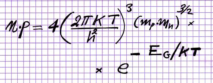
40 Appendix II: Number of Carriers in Semiconductors Fermi Statistics is used to calculate the number of electron and hole carriers in a semiconductor. The explicit calculation is shown 40


41 Appendix II: Number of Carriers in a Semiconductor 41

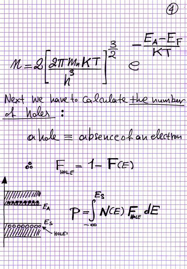
42 Appendix II: II 42

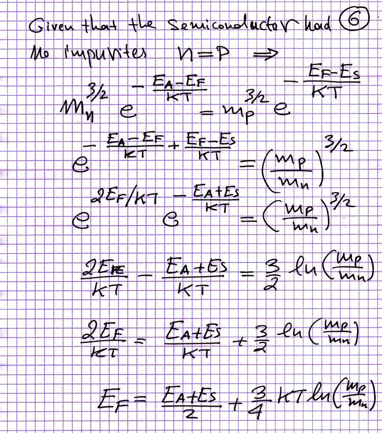
43 Appendix II: III 43

44 Appendix II: IV 44
ECE PN Junctions and Diodes
 ECE 342 2. PN Junctions and iodes Jose E. Schutt-Aine Electrical & Computer Engineering University of Illinois jschutt@emlab.uiuc.edu ECE 342 Jose Schutt Aine 1 B: material dependent parameter = 5.4 10
Basic Physics of Semiconductors
 Basic Physics of Semiconductors Semiconductor materials and their properties PN-junction diodes Reverse Breakdown EEM 205 Electronics I Dicle University, EEE Dr. Mehmet Siraç ÖZERDEM Semiconductor Physics
UNIVERSITY OF CALIFORNIA, BERKELEY College of Engineering Department of Electrical Engineering and Computer Sciences
 UNIVERSITY OF CALIFORNIA, BERKELEY College of Engineering Department of Electrical Engineering and Computer Sciences EE 105: Microelectronic Devices and Circuits Spring 2008 MIDTERM EXAMINATION #1 Time
Diodes. anode. cathode. cut-off. Can be approximated by a piecewise-linear-like characteristic. Lecture 9-1
 Diodes mplest nonlinear circuit element Basic operation sets the foundation for Bipolar Junction Transistors (BJTs) Also present in Field Effect Transistors (FETs) Ideal diode characteristic anode cathode
Electronic Circuits for Mechatronics ELCT 609 Lecture 2: PN Junctions (1)
") Electronic Circuits for Mechatronics ELCT 609 Lecture 2: PN Junctions (1) Assistant Professor Office: C3.315 E-mail: eman.azab@guc.edu.eg 1 Electronic (Semiconductor) Devices P-N Junctions (Diodes): Physical
Electronic Circuits for Mechatronics ELCT 609 Lecture 2: PN Junctions (1) Assistant Professor Office: C3.315 E-mail: eman.azab@guc.edu.eg 1 Electronic (Semiconductor) Devices P-N Junctions (Diodes): Physical
L03: pn Junctions, Diodes
 8/30/2012 Page 1 of 5 Reference:C:\Users\Bernhard Boser\Documents\Files\Lib\MathCAD\Default\defaults.mcd L03: pn Junctions, Diodes Intrinsic Si Q: What are n, p? Q: Is the Si charged? Q: How could we make
Lecture 1. OUTLINE Basic Semiconductor Physics. Reading: Chapter 2.1. Semiconductors Intrinsic (undoped) silicon Doping Carrier concentrations
 silicon Doping Carrier concentrations") Lecture 1 OUTLINE Basic Semiconductor Physics Semiconductors Intrinsic (undoped) silicon Doping Carrier concentrations Reading: Chapter 2.1 EE105 Fall 2007 Lecture 1, Slide 1 What is a Semiconductor? Low
Lecture 1 OUTLINE Basic Semiconductor Physics Semiconductors Intrinsic (undoped) silicon Doping Carrier concentrations Reading: Chapter 2.1 EE105 Fall 2007 Lecture 1, Slide 1 What is a Semiconductor? Low
For the following statements, mark ( ) for true statement and (X) for wrong statement and correct it.
 for true statement and (X) for wrong statement and correct it.") Benha University Faculty of Engineering Shoubra Electrical Engineering Department First Year communications. Answer all the following questions Illustrate your answers with sketches when necessary. The
Benha University Faculty of Engineering Shoubra Electrical Engineering Department First Year communications. Answer all the following questions Illustrate your answers with sketches when necessary. The
PN Junction
 P Junction 2017-05-04 Definition Power Electronics = semiconductor switches are used Analogue amplifier = high power loss 250 200 u x 150 100 u Udc i 50 0 0 50 100 150 200 250 300 350 400 i,u dc i,u u
Quiz #1 Practice Problem Set
 Name: Student Number: ELEC 3908 Physical Electronics Quiz #1 Practice Problem Set? Minutes January 22, 2016 - No aids except a non-programmable calculator - All questions must be answered - All questions
Diodes. EE223 Digital & Analogue Electronics Derek Molloy 2012/2013.
 Diodes EE223 Digital & Analogue Electronics Derek Molloy 2012/2013 Derek.Molloy@dcu.ie Diodes: A Semiconductor? Conductors Such as copper, aluminium have a cloud of free electrons weak bound valence electrons
n N D n p = n i p N A
 Summary of electron and hole concentration in semiconductors Intrinsic semiconductor: E G n kt i = pi = N e 2 0 Donor-doped semiconductor: n N D where N D is the concentration of donor impurity Acceptor-doped
Introduction to Transistors. Semiconductors Diodes Transistors
 Introduction to Transistors Semiconductors Diodes Transistors 1 Semiconductors Typical semiconductors, like silicon and germanium, have four valence electrons which form atomic bonds with neighboring atoms
Charge Carriers in Semiconductor
 Charge Carriers in Semiconductor To understand PN junction s IV characteristics, it is important to understand charge carriers behavior in solids, how to modify carrier densities, and different mechanisms
SEMICONDUCTORS. Conductivity lies between conductors and insulators. The flow of charge in a metal results from the
 SEMICONDUCTORS Conductivity lies between conductors and insulators The flow of charge in a metal results from the movement of electrons Electros are negatively charged particles (q=1.60x10⁻¹⁹ C ) The outermost
Lecture (02) PN Junctions and Diodes
 PN Junctions and Diodes") Lecture (02) PN Junctions and Diodes By: Dr. Ahmed ElShafee ١ I Agenda N type, P type semiconductors N Type Semiconductor P Type Semiconductor PN junction Energy Diagrams of the PN Junction and Depletion
Lecture (02) PN Junctions and Diodes By: Dr. Ahmed ElShafee ١ I Agenda N type, P type semiconductors N Type Semiconductor P Type Semiconductor PN junction Energy Diagrams of the PN Junction and Depletion
Electronics The basics of semiconductor physics
 Electronics The basics of semiconductor physics Prof. Márta Rencz, Gergely Nagy BME DED September 16, 2013 The basic properties of semiconductors Semiconductors conductance is between that of conductors
ECE-342 Test 2 Solutions, Nov 4, :00-8:00pm, Closed Book (one page of notes allowed)
") ECE-342 Test 2 Solutions, Nov 4, 2008 6:00-8:00pm, Closed Book (one page of notes allowed) Please use the following physical constants in your calculations: Boltzmann s Constant: Electron Charge: Free
ECE-342 Test 2 Solutions, Nov 4, 2008 6:00-8:00pm, Closed Book (one page of notes allowed) Please use the following physical constants in your calculations: Boltzmann s Constant: Electron Charge: Free
Lecture (02) Introduction to Electronics II, PN Junction and Diodes I
 Introduction to Electronics II, PN Junction and Diodes I") Lecture (02) Introduction to Electronics II, PN Junction and Diodes I By: Dr. Ahmed ElShafee ١ Agenda Current in semiconductors/conductors N type, P type semiconductors N Type Semiconductor P Type Semiconductor
Lecture (02) Introduction to Electronics II, PN Junction and Diodes I By: Dr. Ahmed ElShafee ١ Agenda Current in semiconductors/conductors N type, P type semiconductors N Type Semiconductor P Type Semiconductor
Semiconductor Physics fall 2012 problems
 Semiconductor Physics fall 2012 problems 1. An n-type sample of silicon has a uniform density N D = 10 16 atoms cm -3 of arsenic, and a p-type silicon sample has N A = 10 15 atoms cm -3 of boron. For each
KATIHAL FİZİĞİ MNT-510
 KATIHAL FİZİĞİ MNT-510 YARIİLETKENLER Kaynaklar: Katıhal Fiziği, Prof. Dr. Mustafa Dikici, Seçkin Yayıncılık Katıhal Fiziği, Şakir Aydoğan, Nobel Yayıncılık, Physics for Computer Science Students: With
Semiconductor Detectors
 Semiconductor Detectors Summary of Last Lecture Band structure in Solids: Conduction band Conduction band thermal conductivity: E g > 5 ev Valence band Insulator Charge carrier in conductor: e - Charge
Lecture 2. Introduction to semiconductors Structures and characteristics in semiconductors
 Lecture 2 Introduction to semiconductors Structures and characteristics in semiconductors Semiconductor p-n junction Metal Oxide Silicon structure Semiconductor contact Literature Glen F. Knoll, Radiation
REVISED HIGHER PHYSICS REVISION BOOKLET ELECTRONS AND ENERGY
 REVSED HGHER PHYSCS REVSON BOOKLET ELECTRONS AND ENERGY Kinross High School Monitoring and measuring a.c. Alternating current: Mains supply a.c.; batteries/cells supply d.c. Electrons moving back and forth,
Semiconductor Physics Problems 2015
 Semiconductor Physics Problems 2015 Page and figure numbers refer to Semiconductor Devices Physics and Technology, 3rd edition, by SM Sze and M-K Lee 1. The purest semiconductor crystals it is possible
Chapter 7. The pn Junction
 Chapter 7 The pn Junction Chapter 7 PN Junction PN junction can be fabricated by implanting or diffusing donors into a P-type substrate such that a layer of semiconductor is converted into N type. Converting
Lecture 2. Introduction to semiconductors Structures and characteristics in semiconductors
 Lecture 2 Introduction to semiconductors Structures and characteristics in semiconductors Semiconductor p-n junction Metal Oxide Silicon structure Semiconductor contact Literature Glen F. Knoll, Radiation
Semiconductors CHAPTER 3. Introduction The pn Junction with an Applied Voltage Intrinsic Semiconductors 136
 CHAPTER 3 Semiconductors Introduction 135 3.1 Intrinsic Semiconductors 136 3.2 Doped Semiconductors 139 3.3 Current Flow in Semiconductors 142 3.4 The pn Junction 148 3.5 The pn Junction with an Applied
Lecture 2. Semiconductor Physics. Sunday 4/10/2015 Semiconductor Physics 1-1
 Lecture 2 Semiconductor Physics Sunday 4/10/2015 Semiconductor Physics 1-1 Outline Intrinsic bond model: electrons and holes Charge carrier generation and recombination Intrinsic semiconductor Doping:
ESE 570: Digital Integrated Circuits and VLSI Fundamentals
 ESE 570: Digital Integrated Circuits and VLSI Fundamentals Lec 4: January 23, 2018 MOS Transistor Theory, MOS Model Penn ESE 570 Spring 2018 Khanna Lecture Outline! CMOS Process Enhancements! Semiconductor
ITT Technical Institute ET215 Devices I Unit 1
 ITT Technical Institute ET215 Devices I Unit 1 Chapter 1 Chapter 2, Sections 2.1-2.4 Chapter 1 Basic Concepts of Analog Circuits Recall ET115 & ET145 Ohms Law I = V/R If voltage across a resistor increases
Solid State Electronics. Final Examination
 The University of Toledo EECS:4400/5400/7400 Solid State Electronic Section elssf08fs.fm - 1 Solid State Electronics Final Examination Problems Points 1. 1. 14 3. 14 Total 40 Was the exam fair? yes no
Session 6: Solid State Physics. Diode
 Session 6: Solid State Physics Diode 1 Outline A B C D E F G H I J 2 Definitions / Assumptions Homojunction: the junction is between two regions of the same material Heterojunction: the junction is between
Classification of Solids
 Classification of Solids Classification by conductivity, which is related to the band structure: (Filled bands are shown dark; D(E) = Density of states) Class Electron Density Density of States D(E) Examples
ECE 340 Lecture 27 : Junction Capacitance Class Outline:
 ECE 340 Lecture 27 : Junction Capacitance Class Outline: Breakdown Review Junction Capacitance Things you should know when you leave M.J. Gilbert ECE 340 Lecture 27 10/24/11 Key Questions What types of
Section 12: Intro to Devices
 Section 12: Intro to Devices Extensive reading materials on reserve, including Robert F. Pierret, Semiconductor Device Fundamentals Bond Model of Electrons and Holes Si Si Si Si Si Si Si Si Si Silicon
ESE 570: Digital Integrated Circuits and VLSI Fundamentals
 ESE 570: Digital Integrated Circuits and VLSI Fundamentals Lec 4: January 29, 2019 MOS Transistor Theory, MOS Model Penn ESE 570 Spring 2019 Khanna Lecture Outline! CMOS Process Enhancements! Semiconductor
3.7 Physical Operation of Diodes
 10/4/2005 3_7 Physical Operation of Diodes blank.doc 1/2 3.7 Physical Operation of Diodes Reading Assignment: pp. 190200, 203205 A. Semiconductor Materials Q: So, what exactly is a junction diode made
Final Examination EE 130 December 16, 1997 Time allotted: 180 minutes
 Final Examination EE 130 December 16, 1997 Time allotted: 180 minutes Problem 1: Semiconductor Fundamentals [30 points] A uniformly doped silicon sample of length 100µm and cross-sectional area 100µm 2
Section 12: Intro to Devices
 Section 12: Intro to Devices Extensive reading materials on reserve, including Robert F. Pierret, Semiconductor Device Fundamentals EE143 Ali Javey Bond Model of Electrons and Holes Si Si Si Si Si Si Si
electronics fundamentals
 electronics fundamentals circuits, devices, and applications THOMAS L. FLOYD DAVID M. BUCHLA Lesson 1: Diodes and Applications Semiconductors Figure 1-1 The Bohr model of an atom showing electrons in orbits
Introduction to Semiconductor Physics. Prof.P. Ravindran, Department of Physics, Central University of Tamil Nadu, India
 Introduction to Semiconductor Physics 1 Prof.P. Ravindran, Department of Physics, Central University of Tamil Nadu, India http://folk.uio.no/ravi/cmp2013 Review of Semiconductor Physics Semiconductor fundamentals
Lecture 2. Introduction to semiconductors Structures and characteristics in semiconductors. Fabrication of semiconductor sensor
 Lecture 2 Introduction to semiconductors Structures and characteristics in semiconductors Semiconductor p-n junction Metal Oxide Silicon structure Semiconductor contact Fabrication of semiconductor sensor
CLASS 12th. Semiconductors
 CLASS 12th Semiconductors 01. Distinction Between Metals, Insulators and Semi-Conductors Metals are good conductors of electricity, insulators do not conduct electricity, while the semiconductors have
Schottky Rectifiers Zheng Yang (ERF 3017,
 ECE442 Power Semiconductor Devices and Integrated Circuits Schottky Rectifiers Zheng Yang (ERF 3017, email: yangzhen@uic.edu) Power Schottky Rectifier Structure 2 Metal-Semiconductor Contact The work function
p-n junction biasing, p-n I-V characteristics, p-n currents Norlaili Mohd. Noh EEE /09
 CLASS 6&7 p-n junction biasing, p-n I-V characteristics, p-n currents 1 p-n junction biasing Unbiased p-n junction: the potential barrier is 0.7 V for Si and 0.3 V for Ge. Nett current across the p-n junction
1 Name: Student number: DEPARTMENT OF PHYSICS AND PHYSICAL OCEANOGRAPHY MEMORIAL UNIVERSITY OF NEWFOUNDLAND. Fall :00-11:00
 1 Name: DEPARTMENT OF PHYSICS AND PHYSICAL OCEANOGRAPHY MEMORIAL UNIVERSITY OF NEWFOUNDLAND Final Exam Physics 3000 December 11, 2012 Fall 2012 9:00-11:00 INSTRUCTIONS: 1. Answer all seven (7) questions.
UNIVERSITY OF CALIFORNIA, BERKELEY College of Engineering Department of Electrical Engineering and Computer Sciences
 UNIVERSITY OF CALIFORNIA, BERKELEY College of Engineering Department of Electrical Engineering and Computer Sciences EECS 40 Spring 2000 Introduction to Microelectronic Devices Prof. King MIDTERM EXAMINATION
Engineering 2000 Chapter 8 Semiconductors. ENG2000: R.I. Hornsey Semi: 1
 Engineering 2000 Chapter 8 Semiconductors ENG2000: R.I. Hornsey Semi: 1 Overview We need to know the electrical properties of Si To do this, we must also draw on some of the physical properties and we
Electro - Principles I
 Electro - Principles I Page 10-1 Atomic Theory It is necessary to know what goes on at the atomic level of a semiconductor so the characteristics of the semiconductor can be understood. In many cases a
A SEMICONDUCTOR DIODE. P-N Junction
 A SEMICONDUCTOR DIODE P-N Junction Analog Electronics Pujianto Department of Physics Edu. State University of Yogyakarta A Semiconductor Devices A Semiconductor devices can be defined as a unit which consists,
ECE 250 Electronic Devices 1. Electronic Device Modeling
 ECE 250 Electronic Devices 1 ECE 250 Electronic Device Modeling ECE 250 Electronic Devices 2 Introduction to Semiconductor Physics You should really take a semiconductor device physics course. We can only
Higher Physics. Electricity. Summary Notes. Monitoring and measuring a.c. Current, potential difference, power and resistance
 Higher Physics Electricity Summary Notes Monitoring and measuring a.c. Current, potential difference, power and resistance Electrical sources and internal resistance Capacitors Conductors, semiconductors
Semiconductor Physics fall 2012 problems
 Semiconductor Physics fall 2012 problems 1. An n-type sample of silicon has a uniform density N D = 10 16 atoms cm -3 of arsenic, and a p-type silicon sample has N A = 10 15 atoms cm -3 of boron. For each
Semiconductor-Detectors
 Semiconductor-Detectors 1 Motivation ~ 195: Discovery that pn-- junctions can be used to detect particles. Semiconductor detectors used for energy measurements ( Germanium) Since ~ 3 years: Semiconductor
Electronic PRINCIPLES
 MALVINO & BATES Electronic PRINCIPLES SEVENTH EDITION Chapter 2 Semiconductors Topics Covered in Chapter 2 Conductors Semiconductors Silicon crystals Intrinsic semiconductors Two types of flow Doping a
Semiconductor Physics and Devices
 The pn Junction 1) Charge carriers crossing the junction. 3) Barrier potential Semiconductor Physics and Devices Chapter 8. The pn Junction Diode 2) Formation of positive and negative ions. 4) Formation
Midterm I - Solutions
 UNIVERSITY OF CALIFORNIA College of Engineering Department of Electrical Engineering and Computer Sciences EECS 130 Spring 2008 Professor Chenming Hu Midterm I - Solutions Name: SID: Grad/Undergrad: Closed
PHYSICAL ELECTRONICS(ECE3540) CHAPTER 9 METAL SEMICONDUCTOR AND SEMICONDUCTOR HETERO-JUNCTIONS
 CHAPTER 9 METAL SEMICONDUCTOR AND SEMICONDUCTOR HETERO-JUNCTIONS") PHYSICAL ELECTRONICS(ECE3540) CHAPTER 9 METAL SEMICONDUCTOR AND SEMICONDUCTOR HETERO-JUNCTIONS Tennessee Technological University Wednesday, October 30, 013 1 Introduction Chapter 4: we considered the
PHYSICAL ELECTRONICS(ECE3540) CHAPTER 9 METAL SEMICONDUCTOR AND SEMICONDUCTOR HETERO-JUNCTIONS Tennessee Technological University Wednesday, October 30, 013 1 Introduction Chapter 4: we considered the
PN Junctions. Lecture 7
 Lecture 7 PN Junctions Kathy Aidala Applied Physics, G2 Harvard University 10 October, 2002 Wei 1 Active Circuit Elements Why are they desirable? Much greater flexibility in circuit applications. What
Solid State Physics SEMICONDUCTORS - IV. Lecture 25. A.H. Harker. Physics and Astronomy UCL
 Solid State Physics SEMICONDUCTORS - IV Lecture 25 A.H. Harker Physics and Astronomy UCL 9.9 Carrier diffusion and recombination Suppose we have a p-type semiconductor, i.e. n h >> n e. (1) Create a local
Silicon Detectors in High Energy Physics
 Thomas Bergauer (HEPHY Vienna) IPM Teheran 22 May 2011 Sunday: Schedule Silicon Detectors in Semiconductor Basics (45 ) Detector concepts: Pixels and Strips (45 ) Coffee Break Strip Detector Performance
Electron Energy, E E = 0. Free electron. 3s Band 2p Band Overlapping energy bands. 3p 3s 2p 2s. 2s Band. Electrons. 1s ATOM SOLID.
 Electron Energy, E Free electron Vacuum level 3p 3s 2p 2s 2s Band 3s Band 2p Band Overlapping energy bands Electrons E = 0 1s ATOM 1s SOLID In a metal the various energy bands overlap to give a single
Review Energy Bands Carrier Density & Mobility Carrier Transport Generation and Recombination
 Review Energy Bands Carrier Density & Mobility Carrier Transport Generation and Recombination The Metal-Semiconductor Junction: Review Energy band diagram of the metal and the semiconductor before (a)
Chapter 1 Overview of Semiconductor Materials and Physics
 Chapter 1 Overview of Semiconductor Materials and Physics Professor Paul K. Chu Conductivity / Resistivity of Insulators, Semiconductors, and Conductors Semiconductor Elements Period II III IV V VI 2 B
! CMOS Process Enhancements. ! Semiconductor Physics. " Band gaps. " Field Effects. ! MOS Physics. " Cut-off. " Depletion.
 ESE 570: Digital Integrated Circuits and VLSI Fundamentals Lec 4: January 3, 018 MOS Transistor Theory, MOS Model Lecture Outline! CMOS Process Enhancements! Semiconductor Physics " Band gaps " Field Effects!
ESE 570: Digital Integrated Circuits and VLSI Fundamentals
 ESE 570: Digital Integrated Circuits and VLSI Fundamentals Lec 4: January 24, 2017 MOS Transistor Theory, MOS Model Penn ESE 570 Spring 2017 Khanna Lecture Outline! Semiconductor Physics " Band gaps "
16EC401 BASIC ELECTRONIC DEVICES UNIT I PN JUNCTION DIODE. Energy Band Diagram of Conductor, Insulator and Semiconductor:
 16EC401 BASIC ELECTRONIC DEVICES UNIT I PN JUNCTION DIODE Energy bands in Intrinsic and Extrinsic silicon: Energy Band Diagram of Conductor, Insulator and Semiconductor: 1 2 Carrier transport: Any motion
The pn junction. [Fonstad, Ghione]
![The pn junction. [Fonstad, Ghione]](/thumbs/93/112370833.jpg "The pn junction. [Fonstad, Ghione]") The pn junction [Fonstad, Ghione] Band diagram On the vertical axis: potential energy of the electrons On the horizontal axis: now there is nothing: later we ll put the position qf s : work function (F
The pn junction [Fonstad, Ghione] Band diagram On the vertical axis: potential energy of the electrons On the horizontal axis: now there is nothing: later we ll put the position qf s : work function (F
SEMICONDUCTOR DIODE. Unbiased (non-polarized) PN junction
 PN junction") SEMICONDUCTOR DIODE Semiconductor diode is an electronic element made of different types of extrinsic semiconductor: N-type semiconductor doped by donor impurities and P-type semiconductor doped by acceptor
SEMICONDUCTOR DIODE Semiconductor diode is an electronic element made of different types of extrinsic semiconductor: N-type semiconductor doped by donor impurities and P-type semiconductor doped by acceptor
ELECTRONIC I Lecture 1 Introduction to semiconductor. By Asst. Prof Dr. Jassim K. Hmood
 ELECTRONIC I Lecture 1 Introduction to semiconductor By Asst. Prof Dr. Jassim K. Hmood SOLID-STATE ELECTRONIC MATERIALS Electronic materials generally can be divided into three categories: insulators,
PN Junction Diode. Diode Cases. Semiconductor Elements. 2009, EE141Associate Professor PhD. T.Vasileva
 PN Junction Diode Semiconductor Elements 1 Diode Cases 2 1 Basic Diode Feature The essential feature of a diode is at e magnitude of e current greatly depends on e polarity of applied voltage. Basicaly
EE 446/646 Photovoltaic Devices I. Y. Baghzouz
 EE 446/646 Photovoltaic Devices I Y. Baghzouz What is Photovoltaics? First used in about 1890, the word has two parts: photo, derived from the Greek word for light, volt, relating to electricity pioneer
! CMOS Process Enhancements. ! Semiconductor Physics. " Band gaps. " Field Effects. ! MOS Physics. " Cut-off. " Depletion.
 ESE 570: Digital Integrated Circuits and VLSI Fundamentals Lec 4: January 9, 019 MOS Transistor Theory, MOS Model Lecture Outline CMOS Process Enhancements Semiconductor Physics Band gaps Field Effects
Semiconductor Devices and Circuits Fall Midterm Exam. Instructor: Dr. Dietmar Knipp, Professor of Electrical Engineering. Name: Mat. -Nr.
 Semiconductor Devices and Circuits Fall 2003 Midterm Exam Instructor: Dr. Dietmar Knipp, Professor of Electrical Engineering Name: Mat. -Nr.: Guidelines: Duration of the Midterm: 1 hour The exam is a closed
Electrical Characteristics of MOS Devices
 Electrical Characteristics of MOS Devices The MOS Capacitor Voltage components Accumulation, Depletion, Inversion Modes Effect of channel bias and substrate bias Effect of gate oide charges Threshold-voltage
The photovoltaic effect occurs in semiconductors where there are distinct valence and
 How a Photovoltaic Cell Works The photovoltaic effect occurs in semiconductors where there are distinct valence and conduction bands. (There are energies at which electrons can not exist within the solid)
UNIVERSITY OF CALIFORNIA College of Engineering Department of Electrical Engineering and Computer Sciences. EECS 130 Professor Ali Javey Fall 2006
 UNIVERSITY OF CALIFORNIA College of Engineering Department of Electrical Engineering and Computer Sciences EECS 130 Professor Ali Javey Fall 2006 Midterm 2 Name: SID: Closed book. Two sheets of notes are
UNIVERSITY OF CALIFORNIA College of Engineering Department of Electrical Engineering and Computer Sciences. EECS 130 Professor Ali Javey Fall 2006
 UNIVERSITY OF CALIFORNIA College of Engineering Department of Electrical Engineering and Computer Sciences EECS 130 Professor Ali Javey Fall 2006 Midterm I Name: Closed book. One sheet of notes is allowed.
Unit IV Semiconductors Engineering Physics
 Introduction A semiconductor is a material that has a resistivity lies between that of a conductor and an insulator. The conductivity of a semiconductor material can be varied under an external electrical
CEMTool Tutorial. Semiconductor physics
 EMTool Tutorial Semiconductor physics Overview This tutorial is part of the EMWARE series. Each tutorial in this series will teach you a specific topic of common applications by explaining theoretical
Qualitative Picture of the Ideal Diode. G.R. Tynan UC San Diego MAE 119 Lecture Notes
 Qualitative Picture of the Ideal Diode G.R. Tynan UC San Diego MAE 119 Lecture Notes Band Theory of Solids: From Single Attoms to Solid Crystals Isolated Li atom (conducting metal) Has well-defined, isolated
EECS130 Integrated Circuit Devices
 EECS130 Integrated Circuit Devices Professor Ali Javey 9/18/2007 P Junctions Lecture 1 Reading: Chapter 5 Announcements For THIS WEEK OLY, Prof. Javey's office hours will be held on Tuesday, Sept 18 3:30-4:30
EE105 Fall 2015 Microelectronic Devices and Circuits: Semiconductor Fabrication and PN Junctions
 EE105 Fall 2015 Microelectronic Devices and Circuits: Semiconductor Fabrication and PN Junctions Prof. Ming C. Wu wu@eecs.berkeley.edu 511 Sutardja Dai Hall (SDH) 1 pn Junction p-type semiconductor in
Semiconductor physics I. The Crystal Structure of Solids
 Lecture 3 Semiconductor physics I The Crystal Structure of Solids 1 Semiconductor materials Types of solids Space lattices Atomic Bonding Imperfection and doping in SOLIDS 2 Semiconductor Semiconductors
Contents CONTENTS. Page 2 of 47
 J. A. Hargreaves Lockerbie Academy June 2015 Contents CONTENTS Contents... 2 CHAPTER 7 CONDUCTORS, SEMICONDUCTORS AND INSULATORS... 4 Summary of Content... 4 Summary of this chapter- notes from column
Chemistry Instrumental Analysis Lecture 8. Chem 4631
 Chemistry 4631 Instrumental Analysis Lecture 8 UV to IR Components of Optical Basic components of spectroscopic instruments: stable source of radiant energy transparent container to hold sample device
Introduction to Semiconductor Devices
 Physics 233 Experiment 48 Introduction to Semiconductor Devices References 1. G.W. Neudeck, The PN Junction Diode, Addison-Wesley MA 1989 2. Background notes (Appendix A) 3. Specification sheet for Diode
Lecture #11. Lecture
 Lecture #11 Semiconductor Diodes and Basic Circuits Outline/Learning Objectives: Simple circuits using ideal diode model, constant voltage drop model, and mathematical (exponential) model. Use of graphical
PHYSICAL ELECTRONICS(ECE3540) CHAPTER 9 METAL SEMICONDUCTOR AND SEMICONDUCTOR HETERO-JUNCTIONS
 CHAPTER 9 METAL SEMICONDUCTOR AND SEMICONDUCTOR HETERO-JUNCTIONS") PHYSICAL ELECTRONICS(ECE3540) CHAPTER 9 METAL SEMICONDUCTOR AND SEMICONDUCTOR HETERO-JUNCTIONS Tennessee Technological University Monday, November 11, 013 1 Introduction Chapter 4: we considered the semiconductor
PHYSICAL ELECTRONICS(ECE3540) CHAPTER 9 METAL SEMICONDUCTOR AND SEMICONDUCTOR HETERO-JUNCTIONS Tennessee Technological University Monday, November 11, 013 1 Introduction Chapter 4: we considered the semiconductor
6.012 Electronic Devices and Circuits
 Page 1 of 1 YOUR NAME Department of Electrical Engineering and Computer Science Massachusetts Institute of Technology 6.12 Electronic Devices and Circuits Exam No. 1 Wednesday, October 7, 29 7:3 to 9:3
Lecture 04 Review of MOSFET
 ECE 541/ME 541 Microelectronic Fabrication Techniques Lecture 04 Review of MOSFET Zheng Yang (ERF 3017, email: yangzhen@uic.edu) What is a Transistor? A Switch! An MOS Transistor V GS V T V GS S Ron D
Energetic particles and their detection in situ (particle detectors) Part II. George Gloeckler
 Part II. George Gloeckler") Energetic particles and their detection in situ (particle detectors) Part II George Gloeckler University of Michigan, Ann Arbor, MI University of Maryland, College Park, MD Simple particle detectors Gas-filled
Energetic particles and their detection in situ (particle detectors) Part II George Gloeckler University of Michigan, Ann Arbor, MI University of Maryland, College Park, MD Simple particle detectors Gas-filled
Spring Semester 2012 Final Exam
 Spring Semester 2012 Final Exam Note: Show your work, underline results, and always show units. Official exam time: 2.0 hours; an extension of at least 1.0 hour will be granted to anyone. Materials parameters
Fundamentals of the Metal Oxide Semiconductor Field-Effect Transistor
 Triode Working FET Fundamentals of the Metal Oxide Semiconductor Field-Effect Transistor The characteristics of energy bands as a function of applied voltage. Surface inversion. The expression for the
Introduction to Semiconductor Devices
 Physics 233 Experiment 48 Introduction to Semiconductor Devices References 1. G.W. Neudeck, The PN Junction Diode, Addison-Wesley MA 1989 2. Background notes (Appendix A) 3. Specification sheet for Diode
Electronic Devices & Circuits
 Electronic Devices & Circuits For Electronics & Communication Engineering By www.thegateacademy.com Syllabus Syllabus for Electronic Devices Energy Bands in Intrinsic and Extrinsic Silicon, Carrier Transport,
Lecture 12: MOS Capacitors, transistors. Context
 Lecture 12: MOS Capacitors, transistors Context In the last lecture, we discussed PN diodes, and the depletion layer into semiconductor surfaces. Small signal models In this lecture, we will apply those
Chapter 1 Semiconductor basics
 Chapter 1 Semiconductor basics ELEC-H402/CH1: Semiconductor basics 1 Basic semiconductor concepts Semiconductor basics Semiconductors, silicon and hole-electron pair Intrinsic silicon properties Doped
Semiconductor Detectors are Ionization Chambers. Detection volume with electric field Energy deposited positive and negative charge pairs
 1 V. Semiconductor Detectors V.1. Principles Semiconductor Detectors are Ionization Chambers Detection volume with electric field Energy deposited positive and negative charge pairs Charges move in field