Single Electron Transistor (SET)
|
|
|
- Claud Lawrence
- 6 years ago
- Views:
Transcription
1 Single Electron Transistor (SET) e - e - dot C g V g A single electron transistor is similar to a normal transistor (below), except 1) the channel is replaced by a small dot. 2) the dot is separated from source and drain by thin insulators. An electron tunnels in two steps: source dot drain source gate channel drain The gate voltage V g is used to control the charge on the gate-dot capacitor C g. How can the charge be controlled with the precision of a single electron? Kouwenhoven et al., Few Electron Quantum Dots, Rep. Prog. Phys. 64, 701 (2001).


2 Designs for Single Electron Transistors Nanoparticle attracted electrostatically to the gap between source and drain electrodes. The gate is underneath.
3 Charging a Dot, One Electron at a Time e - e - dot C g V g Sweeping the gate voltage V g changes the charge Q g on the gate-dot capacitor C g. To add one electron requires the voltage ΔV g e/c g since C g =Q g /V g. The source-drain conductance G is zero for most gate voltages, because putting even one extra electron onto the dot would cost too much Coulomb energy. This is called Coulomb blockade. N-1 Electrons on the dot N-½ N N+½ ΔV g e/c g Electrons can hop onto the dot only at a gate voltage where the number of electrons on the dot flip-flops between N and N+1. Their time-averaged number is N+½ in that case. The spacing between these halfinteger conductance peaks is an integer.
4 The SET as Extremely Sensitive Charge Detector At low temperature, the conductance peaks in a SET become very sharp. Consequently, a very small change in the gate voltage half-way up a peak produces a large current change, i.e. a large amplification. That makes the SET extremely sensitive to tiny charges. The flip side of this sensitivity is that a SET detects every nearby electron. When it hops from one trap to another, the SET produces a noise peak. Sit here:
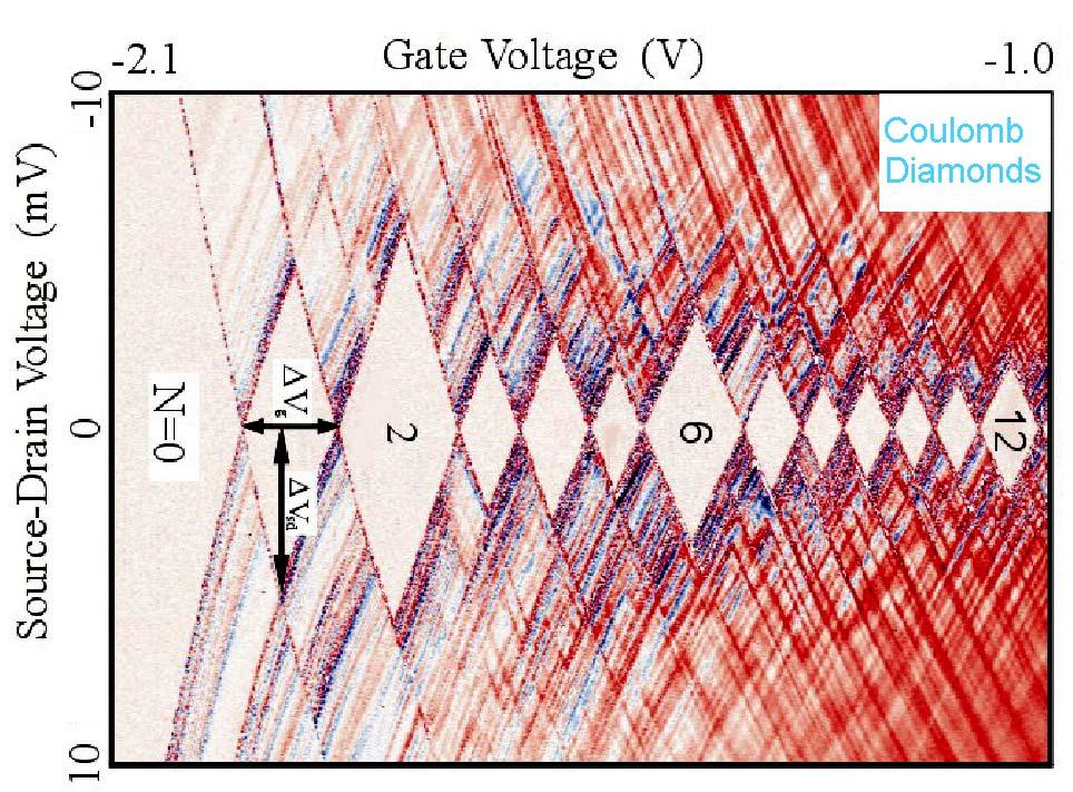
5 Gate Voltage versus Source-Drain Voltage The situation gets a bit confusing, because there are two voltages that can be varied, the gate voltage V g and the source-drain voltage V s-d. Both affect the conductance. Therefore, one often plots the conductance G against both voltages (see the next slide for data). Schematically, one obtains Coulomb diamonds, which are regions with a stable electron number N on the dot (and consequently zero conductance). G 1 /2 3 /2 5 /2 7 /2 V g V s-d V g
6
7 Including the Energy Levels of a Quantum Dot Contrary to the Coulomb blockade model, the data show Coulomb diamonds with uneven size. Some electron numbers have particularly large diamonds, indicating that the corresponding electron number is particularly stable. This is reminiscent of the closed electron shells in atoms. Small dots behave like artificial atoms when their size shrinks down to the electron wavelength. Continuous energy bands become quantized (see Lecture 8). Adding one electron requires the Coulomb energy U plus the difference ΔE between two quantum levels (next slide). If a second electron is added to the same quantum level (the same shell in an atom), ΔE vanishes and only the Coulomb energy U is needed. The quantum energy levels can be extracted from the spacing between the conductance peaks by subtracting the Coulomb energy U = e 2 /C.

8 Quantum Dot in 2D (Disk) Filling the Electron Shells in 2D
9 Shell Structure of Energy Levels for Various Potentials Magic Numbers (in 3D) E Potentials:
 drain (For a detailed explanation see the annotation in the.")
10 Two Step Tunneling source dot drain dot empty empty N+1 filled source N (filled) drain (For a detailed explanation see the annotation in the.ppt version.)

11 Coulomb Energy U Two stable charge states of a dot with N and N+1 electrons are separated by the Coulomb energy U=e 2 /C. The dot capacitance C decreases when shrinking the dot. Consequently, the Coulomb energy U increases. When U exceeds the thermal energy k B T, single electron charging can be detected. At room temperature ( k B T 25 mev ) this requires dots smaller than 10 nm (Lect. 2, Slide 2). Coulomb energy U=e 2 /C of a spherical dot embedded in a medium with dielectric constant ε, with the counter electrode at infinity : 2e 2 /ε d d
12 Conditions for a Coulomb Blockade 1) The Coulomb energy e 2 /C needs to exceed the thermal energy k B T. Otherwise an extra electron can get onto the dot with thermal energy instead of being blocked by the Coulomb energy. A dot needs to be either small (<10 nm at 300K) or cold (< 1K for a μm sized dot). 2) The residence time Δt=RC of an electron on the dot needs to be so long that the corresponding energy uncertainty ΔE=h/Δt = h/rc is less than the Coulomb energy e 2 /C. That leads to a condition for the tunnel resistance between the dot and source/drain: R > h/e 2 26 kω


13 Superconducting SET A superconducting SET sample with a 2 μm long island and 70 nm wide leads. The gate at the bottom allows control of the number of electrons on the island.
14 Superconducting SET Current vs. charge curves for a superconducting dot with normal metals as source and drain. At low temperatures (bottom) the period changes from e to 2e, indicating the involvement of Cooper pairs.

15 Single Electron Turnstile
16 Precision Standards from Single Electronics Count individual electrons, pairs, flux quanta Current I Coulomb Blockade Voltage V Josephson Effect I = e f V = h/2e f V/I = R = h/e 2 Resistance R Quantum Hall Effect (f = frequency)
Single Electron Transistor (SET)
") Single Electron Transistor (SET) SET: e - e - dot A single electron transistor is similar to a normal transistor (below), except 1) the channel is replaced by a small dot. C g 2) the dot is separated from
Single Electron Transistor (SET) SET: e - e - dot A single electron transistor is similar to a normal transistor (below), except 1) the channel is replaced by a small dot. C g 2) the dot is separated from
Coulomb Blockade and Kondo Effect in Nanostructures
 Coulomb Blockade and Kondo Effect in Nanostructures Marcin M. Wysokioski 1,2 1 Institute of Physics Albert-Ludwigs-Universität Freiburg 2 Institute of Physics Jagiellonian University, Cracow, Poland 2.VI.2010
Quantum transport in nanostructures
 Quantum transport in nanostructures About the manifestations of quantum mechanics on the electrical transport properties of conductors V At macro scale I = V/R (Ohm s law) = σv At nano scale I? V Moore
Building blocks for nanodevices
 Building blocks for nanodevices Two-dimensional electron gas (2DEG) Quantum wires and quantum point contacts Electron phase coherence Single-Electron tunneling devices - Coulomb blockage Quantum dots (introduction)
single-electron electron tunneling (SET)
") single-electron electron tunneling (SET) classical dots (SET islands): level spacing is NOT important; only the charging energy (=classical effect, many electrons on the island) quantum dots: : level spacing
single-electron electron tunneling (SET) classical dots (SET islands): level spacing is NOT important; only the charging energy (=classical effect, many electrons on the island) quantum dots: : level spacing
Electronic transport in low dimensional systems
 Electronic transport in low dimensional systems For example: 2D system l
Nanoelectronics. Topics
 Nanoelectronics Topics Moore s Law Inorganic nanoelectronic devices Resonant tunneling Quantum dots Single electron transistors Motivation for molecular electronics The review article Overview of Nanoelectronic
Fig. 8.1 : Schematic for single electron tunneling arrangement. For large system this charge is usually washed out by the thermal noise
 Part 2 : Nanostuctures Lecture 1 : Coulomb blockade and single electron tunneling Module 8 : Coulomb blockade and single electron tunneling Coulomb blockade and single electron tunneling A typical semiconductor
Lectures: Condensed Matter II 1 Electronic Transport in Quantum dots 2 Kondo effect: Intro/theory. 3 Kondo effect in nanostructures
 Lectures: Condensed Matter II 1 Electronic Transport in Quantum dots 2 Kondo effect: Intro/theory. 3 Kondo effect in nanostructures Luis Dias UT/ORNL Lectures: Condensed Matter II 1 Electronic Transport
No reason one cannot have double-well structures: With MBE growth, can control well thicknesses and spacings at atomic scale.
 The story so far: Can use semiconductor structures to confine free carriers electrons and holes. Can get away with writing Schroedinger-like equation for Bloch envelope function to understand, e.g., -confinement
ESE370: Circuit-Level Modeling, Design, and Optimization for Digital Systems
 ESE370: Circuit-Level Modeling, Design, and Optimization for Digital Systems Lec 6: September 14, 2015 MOS Model You are Here: Transistor Edition! Previously: simple models (0 and 1 st order) " Comfortable
Fabrication / Synthesis Techniques
 Quantum Dots Physical properties Fabrication / Synthesis Techniques Applications Handbook of Nanoscience, Engineering, and Technology Ch.13.3 L. Kouwenhoven and C. Marcus, Physics World, June 1998, p.35
ESE370: Circuit-Level Modeling, Design, and Optimization for Digital Systems. Today MOS MOS. Capacitor. Idea
 ESE370: Circuit-Level Modeling, Design, and Optimization for Digital Systems Day 9: September 26, 2011 MOS Model Today MOS Structure Basic Idea Semiconductor Physics Metals, insulators Silicon lattice
! Previously: simple models (0 and 1 st order) " Comfortable with basic functions and circuits. ! This week and next (4 lectures)
 Comfortable with basic functions and circuits. ! This week and next (4 lectures)") ESE370: CircuitLevel Modeling, Design, and Optimization for Digital Systems Lec 6: September 14, 2015 MOS Model You are Here: Transistor Edition! Previously: simple models (0 and 1 st order) " Comfortable
ESE370: CircuitLevel Modeling, Design, and Optimization for Digital Systems Lec 6: September 14, 2015 MOS Model You are Here: Transistor Edition! Previously: simple models (0 and 1 st order) " Comfortable
Transport through Andreev Bound States in a Superconductor-Quantum Dot-Graphene System
 Transport through Andreev Bound States in a Superconductor-Quantum Dot-Graphene System Nadya Mason Travis Dirk, Yung-Fu Chen, Cesar Chialvo Taylor Hughes, Siddhartha Lal, Bruno Uchoa Paul Goldbart University
ESE370: Circuit-Level Modeling, Design, and Optimization for Digital Systems
 ESE370: Circuit-Level Modeling, Design, and Optimization for Digital Systems Lec 6: September 18, 2017 MOS Model You are Here: Transistor Edition! Previously: simple models (0 and 1 st order) " Comfortable
Lecture 20: Semiconductor Structures Kittel Ch 17, p , extra material in the class notes
 Lecture 20: Semiconductor Structures Kittel Ch 17, p 494-503, 507-511 + extra material in the class notes MOS Structure Layer Structure metal Oxide insulator Semiconductor Semiconductor Large-gap Semiconductor
Counting Individual Electrons on Liquid Helium
 Counting Individual Electrons on Liquid Helium G. Papageorgiou 1, P. Glasson 1, K. Harrabi 1, V.Antonov 1, E.Collin 2, P.Fozooni 1, P.G.Frayne 1, M.J.Lea 1, Y.Mukharsky 2 and D.G.Rees 1. 1 Department of
Lecture 8, April 12, 2017
 Lecture 8, April 12, 2017 This week (part 2): Semiconductor quantum dots for QIP Introduction to QDs Single spins for qubits Initialization Read-Out Single qubit gates Book on basics: Thomas Ihn, Semiconductor
Lecture 20 - Semiconductor Structures
 Lecture 0: Structures Kittel Ch 17, p 494-503, 507-511 + extra material in the class notes MOS Structure metal Layer Structure Physics 460 F 006 Lect 0 1 Outline What is a semiconductor Structure? Created
Solids. Solids are everywhere. Looking around, we see solids. Composite materials make airplanes and cars lighter, golf clubs more powerful,
 Solids Solids are everywhere. Looking around, we see solids. Most of our electronics is solid state. Composite materials make airplanes and cars lighter, golf clubs more powerful, In addition to hard matter
GRAPHENE the first 2D crystal lattice
 GRAPHENE the first 2D crystal lattice dimensionality of carbon diamond, graphite GRAPHENE realized in 2004 (Novoselov, Science 306, 2004) carbon nanotubes fullerenes, buckyballs what s so special about
Classification of Solids
 Classification of Solids Classification by conductivity, which is related to the band structure: (Filled bands are shown dark; D(E) = Density of states) Class Electron Density Density of States D(E) Examples
Temperature dependence of Andreev spectra in a superconducting carbon nanotube quantum dot
 Temperature dependence of Andreev spectra in a superconducting carbon nanotube quantum dot A. Kumar, M. Gaim, D. Steininger, A. Levy Yeyati, A. Martín-Rodero, A. K. Hüttel, and C. Strunk Phys. Rev. B 89,
! Previously: simple models (0 and 1 st order) " Comfortable with basic functions and circuits. ! This week and next (4 lectures)
 Comfortable with basic functions and circuits. ! This week and next (4 lectures)") ESE370: CircuitLevel Modeling, Design, and Optimization for Digital Systems Lec 6: September 18, 2017 MOS Model You are Here: Transistor Edition! Previously: simple models (0 and 1 st order) " Comfortable
ESE370: CircuitLevel Modeling, Design, and Optimization for Digital Systems Lec 6: September 18, 2017 MOS Model You are Here: Transistor Edition! Previously: simple models (0 and 1 st order) " Comfortable
Solid-State Spin Quantum Computers
 Solid-State Spin Quantum Computers 1 NV-Centers in Diamond P Donors in Silicon Kane s Computer (1998) P- doped silicon with metal gates Silicon host crystal + 31 P donor atoms + Addressing gates + J- coupling
SUPPLEMENTARY INFORMATION
 SUPPLEMENTARY INFORMATION Flexible, high-performance carbon nanotube integrated circuits Dong-ming Sun, Marina Y. Timmermans, Ying Tian, Albert G. Nasibulin, Esko I. Kauppinen, Shigeru Kishimoto, Takashi
Introduction)! Electrostatics is the study of stationary electric charges and fields (as opposed to moving charges and currents)
! Electrostatics is the study of stationary electric charges and fields (as opposed to moving charges and currents)") Higher'Physics'1B Electricity) Electrostatics)) Introduction) Electrostatics is the study of stationary electric charges and fields (as opposed to moving charges and currents) Properties)of)Electric)Charges)
Higher'Physics'1B Electricity) Electrostatics)) Introduction) Electrostatics is the study of stationary electric charges and fields (as opposed to moving charges and currents) Properties)of)Electric)Charges)
Electronic Quantum Transport in Mesoscopic Semiconductor Structures
 Thomas Ihn Electronic Quantum Transport in Mesoscopic Semiconductor Structures With 90 Illustrations, S in Full Color Springer Contents Part I Introduction to Electron Transport l Electrical conductance
Demonstration of a functional quantum-dot cellular automata cell
 Demonstration of a functional quantum-dot cellular automata cell Islamshah Amlani, a) Alexei O. Orlov, Gregory L. Snider, Craig S. Lent, and Gary H. Bernstein Department of Electrical Engineering, University
Analysis of flip flop design using nanoelectronic single electron transistor
 Int. J. Nanoelectronics and Materials 10 (2017) 21-28 Analysis of flip flop design using nanoelectronic single electron transistor S.Rajasekaran*, G.Sundari Faculty of Electronics Engineering, Sathyabama
Quantum-dot cellular automata
 Quantum-dot cellular automata G. L. Snider, a) A. O. Orlov, I. Amlani, X. Zuo, G. H. Bernstein, C. S. Lent, J. L. Merz, and W. Porod Department of Electrical Engineering, University of Notre Dame, Notre
Single-Electron Tunneling
 247 9 Single-Electron Tunneling The charge stored on a capacitor is not quantized: it consists of polarization charges generated by displacing the electron gas with respect to the positive lattice ions
M.C. Escher. Angels and devils (detail), 1941
, 1941") M.C. Escher Angels and devils (detail), 1941 1 Coherent Quantum Phase Slip: Exact quantum dual to Josephson Tunneling (Coulomb blockade is a partial dual) Degree of freedom in superconductor: Phase and
M.C. Escher Angels and devils (detail), 1941 1 Coherent Quantum Phase Slip: Exact quantum dual to Josephson Tunneling (Coulomb blockade is a partial dual) Degree of freedom in superconductor: Phase and
Supercondcting Qubits
 Supercondcting Qubits Patricia Thrasher University of Washington, Seattle, Washington 98195 Superconducting qubits are electrical circuits based on the Josephson tunnel junctions and have the ability to
Lecture 2 Thin Film Transistors
 Lecture 2 Thin Film Transistors 1/60 Announcements Homework 1/4: Will be online after the Lecture on Tuesday October 2 nd. Total of 25 marks. Each homework contributes an equal weight. All homework contributes
ELECTRON TRANSPORT IN SEMICONDUCTOR QUANTUM DOTS. University of Technology, P.O. Box 5046, 2600 GA DELFT, The Netherlands
 ELECTRON TRANSPORT IN SEMICONDUCTOR QUANTUM DOTS Seigo Tarucha 1, 2, David Guy Austing 2 and Toshimasa Fujisawa 2 and L.P. Kouwenhoven 3 1 Department of Physics and ERATO Mesoscopic Correlation Project
Single-Electron Devices
 Single-Electron Devices Jürgen Weis Max-Planck-Institut für Festkörperforschung, Heisenbergstr. 1, 7569 Stuttgart, Germany 1 Introduction The electrical charge is quantized in the elementary quantum e
Lecture 17 Field-Effect Transistors 2
 Lecture 17 Field-Effect Transistors chroder: Chapters, 4, 6 1/57 Announcements Homework 4/6: Is online now. ue Monday May 1st at 10:00am. I will return it the following Monday (8 th May). Homework 5/6:
Information processing in nanoscale systems
 Information processing in nanoscale systems Mark Rudner Niels Bohr International Academy Image from: www.upscale.utoronto.ca 100 years after Bohr, the basic laws and players are established 1913 2013 Image
EN2912C: Future Directions in Computing Lecture 08: Overview of Near-Term Emerging Computing Technologies
 EN2912C: Future Directions in Computing Lecture 08: Overview of Near-Term Emerging Computing Technologies Prof. Sherief Reda Division of Engineering Brown University Fall 2008 1 Near-term emerging computing
SUPPLEMENTARY INFORMATION
 Collapse of superconductivity in a hybrid tin graphene Josephson junction array by Zheng Han et al. SUPPLEMENTARY INFORMATION 1. Determination of the electronic mobility of graphene. 1.a extraction from
Electrostatics of Nanowire Transistors
 Electrostatics of Nanowire Transistors Jing Guo, Jing Wang, Eric Polizzi, Supriyo Datta and Mark Lundstrom School of Electrical and Computer Engineering Purdue University, West Lafayette, IN, 47907 ABSTRACTS
Single Electron Tunneling Examples
 Single Electron Tunneling Examples Danny Porath 2002 (Schönenberger et. al.) It has long been an axiom of mine that the little things are infinitely the most important Sir Arthur Conan Doyle Books and
Charge spectrometry with a strongly coupled superconducting single-electron transistor
 PHYSICAL REVIEW B, VOLUME 64, 245116 Charge spectrometry with a strongly coupled superconducting single-electron transistor C. P. Heij, P. Hadley, and J. E. Mooij Applied Physics and Delft Institute of
SPIN-POLARIZED CURRENT IN A MAGNETIC TUNNEL JUNCTION: MESOSCOPIC DIODE BASED ON A QUANTUM DOT
 66 Rev.Adv.Mater.Sci. 14(2007) 66-70 W. Rudziński SPIN-POLARIZED CURRENT IN A MAGNETIC TUNNEL JUNCTION: MESOSCOPIC DIODE BASED ON A QUANTUM DOT W. Rudziński Department of Physics, Adam Mickiewicz University,
Coulomb blockade in metallic islands and quantum dots
 Coulomb blockade in metallic islands and quantum dots Charging energy and chemical potential of a metallic island Coulomb blockade and single-electron transistors Quantum dots and the constant interaction
Quantum Information Processing with Semiconductor Quantum Dots
 Quantum Information Processing with Semiconductor Quantum Dots slides courtesy of Lieven Vandersypen, TU Delft Can we access the quantum world at the level of single-particles? in a solid state environment?
Mesoscopic Nano-Electro-Mechanics of Shuttle Systems
 * Mesoscopic Nano-Electro-Mechanics of Shuttle Systems Robert Shekhter University of Gothenburg, Sweden Lecture1: Mechanically assisted single-electronics Lecture2: Quantum coherent nano-electro-mechanics
Lecture 2, March 2, 2017
 Lecture 2, March 2, 2017 Last week: Introduction to topics of lecture Algorithms Physical Systems The development of Quantum Information Science Quantum physics perspective Computer science perspective
Lecture 5: CMOS Transistor Theory
 Lecture 5: CMOS Transistor Theory Slides courtesy of Deming Chen Slides based on the initial set from David Harris CMOS VLSI Design Outline q q q q q q q Introduction MOS Capacitor nmos I-V Characteristics
Supplementary Information
 Supplementary Information Quantum supercurrent transistors in carbon nanotubes Pablo Jarillo-Herrero, Jorden A. van Dam, Leo P. Kouwenhoven Device Fabrication The nanotubes were grown by chemical vapour
Lecture 18 Field-Effect Transistors 3
 Lecture 18 Field-Effect Transistors 3 Schroder: Chapters, 4, 6 1/38 Announcements Homework 4/6: Is online now. Due Today. I will return it next Wednesday (30 th May). Homework 5/6: It will be online later
The Nanotube SQUID. uhu,, M. Monthioux,, V. Bouchiat, W. Wernsdorfer, CEMES-Toulouse, CRTBT & LLN Grenoble
 The Nanotube SQUID J.-P. Cleuziou,, Th. Ondarçuhu uhu,, M. Monthioux,, V. Bouchiat, W. Wernsdorfer, CEMES-Toulouse, CRTBT & LLN Grenoble Outline Sample fabrication Proximity effect in CNT The CNT superconducting
Class 05: Device Physics II
 Topics: 1. Introduction 2. NFET Model and Cross Section with Parasitics 3. NFET as a Capacitor 4. Capacitance vs. Voltage Curves 5. NFET as a Capacitor - Band Diagrams at V=0 6. NFET as a Capacitor - Accumulation
THE UNIVERSITY OF NEW SOUTH WALES SCHOOL OF PHYSICS FINAL EXAMINATION JUNE/JULY PHYS3080 Solid State Physics
 THE UNIVERSITY OF NEW SOUTH WALES SCHOOL OF PHYSICS FINAL EXAMINATION JUNE/JULY 006 PHYS3080 Solid State Physics Time Allowed hours Total number of questions - 5 Answer ALL questions All questions are
(a) (b) Supplementary Figure 1. (a) (b) (a) Supplementary Figure 2. (a) (b) (c) (d) (e)
 (b) Supplementary Figure 1. (a) (b) (a) Supplementary Figure 2. (a) (b) (c) (d) (e)") (a) (b) Supplementary Figure 1. (a) An AFM image of the device after the formation of the contact electrodes and the top gate dielectric Al 2 O 3. (b) A line scan performed along the white dashed line
(a) (b) Supplementary Figure 1. (a) An AFM image of the device after the formation of the contact electrodes and the top gate dielectric Al 2 O 3. (b) A line scan performed along the white dashed line
Quantum Information Processing with Semiconductor Quantum Dots. slides courtesy of Lieven Vandersypen, TU Delft
 Quantum Information Processing with Semiconductor Quantum Dots slides courtesy of Lieven Vandersypen, TU Delft Can we access the quantum world at the level of single-particles? in a solid state environment?
Quantum physics in quantum dots
 Quantum physics in quantum dots Klaus Ensslin Solid State Physics Zürich AFM nanolithography Multi-terminal tunneling Rings and dots Time-resolved charge detection Moore s Law Transistors per chip 10 9
Capacitors II. Physics 2415 Lecture 9. Michael Fowler, UVa
 Capacitors II Physics 2415 Lecture 9 Michael Fowler, UVa Today s Topics First, some review then Storing energy in a capacitor How energy is stored in the electric field Dielectrics: why they strengthen
Formation of unintentional dots in small Si nanostructures
 Superlattices and Microstructures, Vol. 28, No. 5/6, 2000 doi:10.1006/spmi.2000.0942 Available online at http://www.idealibrary.com on Formation of unintentional dots in small Si nanostructures L. P. ROKHINSON,
Coulomb Blockade IV characteristics in. (La,Pr,Ca)MnO3
MnO3") Coulomb Blockade IV characteristics in (La,Pr,Ca)MnO3 Sarah Joy Advisor: Dr. Selman Hershfield 2008 REU University of Florida July 29, 2008 Abstract In a sample of manganite at 70K, ferromagnetic islands
Coulomb Blockade IV characteristics in (La,Pr,Ca)MnO3 Sarah Joy Advisor: Dr. Selman Hershfield 2008 REU University of Florida July 29, 2008 Abstract In a sample of manganite at 70K, ferromagnetic islands
Enhancement-mode quantum transistors for single electron spin
 Purdue University Purdue e-pubs Other Nanotechnology Publications Birck Nanotechnology Center 8-1-2006 Enhancement-mode quantum transistors for single electron spin G. M. Jones B. H. Hu C. H. Yang M. J.
SUPPLEMENTARY INFORMATION
 Electrical control of single hole spins in nanowire quantum dots V. S. Pribiag, S. Nadj-Perge, S. M. Frolov, J. W. G. van den Berg, I. van Weperen., S. R. Plissard, E. P. A. M. Bakkers and L. P. Kouwenhoven
Stability Diagram of a Few-Electron Triple Dot
 Stability Diagram of a Few-Electron Triple Dot L. Gaudreau Institute For Microstructural Sciences, NRC, Ottawa, Canada K1A 0R6 Régroupement Québécois sur les Matériaux de Pointe, Université de Sherbrooke,
Observation of ionic Coulomb blockade in nanopores
 Observation of ionic Coulomb blockade in nanopores Jiandong Feng 1 *, Ke Liu 1, Michael Graf 1, Dumitru Dumcenco 2, Andras Kis 2, Massimiliano Di Ventra 3, & Aleksandra Radenovic 1 * 1 Laboratory of Nanoscale
Herre van der Zant. interplay between molecular spin and electron transport (molecular spintronics) Gate
 Gate") transport through the single molecule magnet Mn12 Herre van der Zant H.B. Heersche, Z. de Groot (Delft) C. Romeike, M. Wegewijs (RWTH Aachen) D. Barreca, E. Tondello (Padova) L. Zobbi, A. Cornia (Modena)
transport through the single molecule magnet Mn12 Herre van der Zant H.B. Heersche, Z. de Groot (Delft) C. Romeike, M. Wegewijs (RWTH Aachen) D. Barreca, E. Tondello (Padova) L. Zobbi, A. Cornia (Modena)
Superconductivity at nanoscale
 Superconductivity at nanoscale Superconductivity is the result of the formation of a quantum condensate of paired electrons (Cooper pairs). In small particles, the allowed energy levels are quantized and
Lecture 2, March 1, 2018
 Lecture 2, March 1, 2018 Last week: Introduction to topics of lecture Algorithms Physical Systems The development of Quantum Information Science Quantum physics perspective Computer science perspective
PHYS102 - Gauss s Law.
 PHYS102 - Gauss s Law. Dr. Suess February 2, 2007 PRS Questions 2 Question #1.............................................................................. 2 Answer to Question #1......................................................................
THEORETICAL DESCRIPTION OF SHELL FILLING IN CYLINDRICAL QUANTUM DOTS
 Vol. 94 (1998) ACTA PHYSICA POLONICA A No. 3 Proc. of the XXVII Intern. School on Physics of Semiconducting Compounds, Jaszowiec 1998 THEORETICAL DESCRIPTION OF SHELL FILLING IN CYLINDRICAL QUANTUM DOTS
Determination of the tunnel rates through a few-electron quantum dot
 Determination of the tunnel rates through a few-electron quantum dot R. Hanson 1,I.T.Vink 1, D.P. DiVincenzo 2, L.M.K. Vandersypen 1, J.M. Elzerman 1, L.H. Willems van Beveren 1 and L.P. Kouwenhoven 1
Dissipation in Transmon
 Dissipation in Transmon Muqing Xu, Exchange in, ETH, Tsinghua University Muqing Xu 8 April 2016 1 Highlight The large E J /E C ratio and the low energy dispersion contribute to Transmon s most significant
Charging and Kondo Effects in an Antidot in the Quantum Hall Regime
 Semiconductor Physics Group Cavendish Laboratory University of Cambridge Charging and Kondo Effects in an Antidot in the Quantum Hall Regime M. Kataoka C. J. B. Ford M. Y. Simmons D. A. Ritchie University
Electronic Devices & Circuits
 Electronic Devices & Circuits For Electronics & Communication Engineering By www.thegateacademy.com Syllabus Syllabus for Electronic Devices Energy Bands in Intrinsic and Extrinsic Silicon, Carrier Transport,
Lecture 6: 2D FET Electrostatics
 Lecture 6: 2D FET Electrostatics 2016-02-01 Lecture 6, High Speed Devices 2014 1 Lecture 6: III-V FET DC I - MESFETs Reading Guide: Liu: 323-337 (he mainly focuses on the single heterostructure FET) Jena:
Chapter 3 Properties of Nanostructures
 Chapter 3 Properties of Nanostructures In Chapter 2, the reduction of the extent of a solid in one or more dimensions was shown to lead to a dramatic alteration of the overall behavior of the solids. Generally,
Nano devices for single photon source and qubit
 Nano devices for single photon source and qubit, Acknowledgement K. Gloos, P. Utko, P. Lindelof Niels Bohr Institute, Denmark J. Toppari, K. Hansen, S. Paraoanu, J. Pekola University of Jyvaskyla, Finland
Observation of switching in a quantum-dot cellular automata cell
 Nanotechnology 10 (1999) 166 173. Printed in the UK PII: S0957-4484(99)97404-4 Observation of switching in a quantum-dot cellular automata cell Gary H Bernstein, Islamshah Amlani, Alexei O Orlov, Craig
chiral m = n Armchair m = 0 or n = 0 Zigzag m n Chiral Three major categories of nanotube structures can be identified based on the values of m and n
 zigzag armchair Three major categories of nanotube structures can be identified based on the values of m and n m = n Armchair m = 0 or n = 0 Zigzag m n Chiral Nature 391, 59, (1998) chiral J. Tersoff,
Review. Spring Semester /21/14. Physics for Scientists & Engineers 2 1
 Review Spring Semester 2014 Physics for Scientists & Engineers 2 1 Notes! Homework set 13 extended to Tuesday, 4/22! Remember to fill out SIRS form: https://sirsonline.msu.edu Physics for Scientists &
Coulomb blockade and single electron tunnelling
 Coulomb blockade and single electron tunnelling Andrea Donarini Institute of theoretical physics, University of Regensburg Three terminal device Source System Drain Gate Variation of the electrostatic
CBSE 12th Physics 2016 Unsolved Paper Delhi Board ARYAN INSTITUTE
 CBSE 12th Physics 2016 Unsolved Paper Delhi Board CBSE 12th Physics 2016 Unsolved Paper Delhi Board TIME - 3HR. QUESTIONS - 26 THE MARKS ARE MENTIONED ON EACH QUESTION SECTION-A Q.1. A point charge +Q
Carbon Nanotubes part 2 CNT s s as a toy model for basic science. Niels Bohr Institute School 2005
 Carbon Nanotubes part 2 CNT s s as a toy model for basic science Niels Bohr Institute School 2005 1 Carbon Nanotubes as a model system 2 Christian Schönenberger University of Basel B. Babic W. Belzig M.
Physics 115. Energy in E fields Electric Current Batteries Resistance. General Physics II. Session 21
 Physics 115 General Physics II Session 21 Energy in E fields Electric Current Batteries Resistance R. J. Wilkes Email: phy115a@u.washington.edu Home page: http://courses.washington.edu/phy115a/ 5/6/14
Single Electron transistors (SET) are one of the possible
 are one of the possible") Modulation of Coulomb Blockade Behavior of Room Temperature Operational Single Electron Transistors by Tunnel Junction P. Santosh Kumar Karre 1, Student Member, IEEE, Aditya Kapoor 2, Govind Mallick 3,
Modulation of Coulomb Blockade Behavior of Room Temperature Operational Single Electron Transistors by Tunnel Junction P. Santosh Kumar Karre 1, Student Member, IEEE, Aditya Kapoor 2, Govind Mallick 3,
Electrical Control of Single Spins in Semiconductor Quantum Dots Jason Petta Physics Department, Princeton University
 Electrical Control of Single Spins in Semiconductor Quantum Dots Jason Petta Physics Department, Princeton University g Q 2 m T + S Mirror U 3 U 1 U 2 U 3 Mirror Detector See Hanson et al., Rev. Mod. Phys.
Large Storage Window in a-sinx/nc-si/a-sinx Sandwiched Structure
 2017 Asia-Pacific Engineering and Technology Conference (APETC 2017) ISBN: 978-1-60595-443-1 Large Storage Window in a-sinx/nc-si/a-sinx Sandwiched Structure Xiang Wang and Chao Song ABSTRACT The a-sin
Quantum Confinement in Graphene
 Quantum Confinement in Graphene from quasi-localization to chaotic billards MMM dominikus kölbl 13.10.08 1 / 27 Outline some facts about graphene quasibound states in graphene numerical calculation of
EE141- Fall 2002 Lecture 27. Memory EE141. Announcements. We finished all the labs No homework this week Projects are due next Tuesday 9am EE141
 - Fall 2002 Lecture 27 Memory Announcements We finished all the labs No homework this week Projects are due next Tuesday 9am 1 Today s Lecture Memory:» SRAM» DRAM» Flash Memory 2 Floating-gate transistor
Supporting Online Material for
 www.sciencemag.org/cgi/content/full/320/5874/356/dc1 Supporting Online Material for Chaotic Dirac Billiard in Graphene Quantum Dots L. A. Ponomarenko, F. Schedin, M. I. Katsnelson, R. Yang, E. W. Hill,
FABRICATION AND CHARACTERIZATION OF SINGLE ELECTRON DEVICE AND STUDY OF ENERGY FILTERING IN SINGLE ELECTRON TRANSPORT LIANG-CHIEH MA
 FABRICATION AND CHARACTERIZATION OF SINGLE ELECTRON DEVICE AND STUDY OF ENERGY FILTERING IN SINGLE ELECTRON TRANSPORT by LIANG-CHIEH MA Presented to the Faculty of the Graduate School of The University
Lecture 9 Superconducting qubits Ref: Clarke and Wilhelm, Nature 453, 1031 (2008).
.") Lecture 9 Superconducting qubits Ref: Clarke and Wilhelm, Nature 453, 1031 (2008). Newcomer in the quantum computation area ( 2000, following experimental demonstration of coherence in charge + flux qubits).
Lecture 9 Superconducting qubits Ref: Clarke and Wilhelm, Nature 453, 1031 (2008). Newcomer in the quantum computation area ( 2000, following experimental demonstration of coherence in charge + flux qubits).
MOS Capacitors ECE 2204
 MOS apacitors EE 2204 Some lasses of Field Effect Transistors Metal-Oxide-Semiconductor Field Effect Transistor MOSFET, which will be the type that we will study in this course. Metal-Semiconductor Field
From nanophysics research labs to cell phones. Dr. András Halbritter Department of Physics associate professor
 From nanophysics research labs to cell phones Dr. András Halbritter Department of Physics associate professor Curriculum Vitae Birth: 1976. High-school graduation: 1994. Master degree: 1999. PhD: 2003.
Sharpen thinking about connections among electric field, electric potential difference, potential energy
 PHYS 2015 -- Week 6 Sharpen thinking about connections among electric field, electric potential difference, potential energy Apply the ideas to capacitance and the parallel plate capacitor For exclusive
From Last Time. Partially full bands = metal Bands completely full or empty = insulator / seminconductor
 From Last Time Solids are large numbers of atoms arranged in a regular crystal structure. Each atom has electron quantum states, but interactions shift the energies. End result is each type atomic electron
Shell-Filling Effects in Circular Quantum Dots
 VLSI DESIGN 1998, Vol. 8, Nos. (1-4), pp. 443-447 Reprints available directly from the publisher Photocopying permitted by license only (C) 1998 OPA (Overseas Publishers Association) N.V. Published by
ECE 340 Lecture 39 : MOS Capacitor II
 ECE 340 Lecture 39 : MOS Capacitor II Class Outline: Effects of Real Surfaces Threshold Voltage MOS Capacitance-Voltage Analysis Things you should know when you leave Key Questions What are the effects
Three-terminal quantum-dot thermoelectrics
 Three-terminal quantum-dot thermoelectrics Björn Sothmann Université de Genève Collaborators: R. Sánchez, A. N. Jordan, M. Büttiker 5.11.2013 Outline Introduction Quantum dots and Coulomb blockade Quantum