Edgeless sensors for full-field X-ray imaging
|
|
|
- Derick Smith
- 6 years ago
- Views:
Transcription

1 Edgeless sensors for full-field X-ray imaging 12 th iworid in Cambridge July 14 th, 2010 Marten Bosma 12 th iworid, Cambridge - July 14 th, 2010
 High detective quantum efficiency Good charge")
 Good spectrometric properties Medipix 3 12 th iworid, Cambridge - July")
2 Human X-ray imaging High spatial resolution Low-contrast resolution High dynamic range Medipix Good noise performance Human X-ray imaging ( kev) High detective quantum efficiency Good charge collection efficiency Good quality high-z sensors High absorption (CdTe-based) Full field imaging Large area (edgeless detectors) Good spectrometric properties Medipix 3 12 th iworid, Cambridge - July 14 th, 2010

3 Current status Four Medipix chips underneath one large sensor (Quad module). ~ 7.5 cm Four Quads in one cooling rig. ~ 0.5 cm Inactive seam of ~ 0.5 cm along one dimension. 12 th iworid, Cambridge - July 14 th, 2010


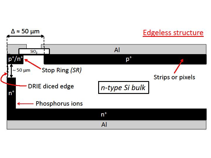
4 Edgeless modules Quad Sensor with Guard Ring Medipix ASIC Medipix ASIC PCB Ball-Grid-Array Through-Silicon-Via Medipix ASIC Edgeless Quad Sensor Medipix ASIC PCB
 Design: Active edge Current termination (stop ring) Pixel Detectors")
5 Edge termination Edge issues: Minimization of charge injection; Confinement of the depletion region; Prevention of high-field regions. Edgeless reduction of inactive periphery by: Less-deleterious dicing: Etching Laser dicing (stealth dicing) Design: Active edge Current termination (stop ring) Pixel Detectors Rossi 12 th iworid, Cambridge - July 14 th, 2010
6 Separation steps 1 st etch (SF 6 C 4 F 8 SF 6 etc.) 1. p + n + n-type Si bulk 2. phosphorus diffusion for: ii. i. Edge activation Surface state passivation Mask material 3. Phosphorus (n + ) 2 nd etch
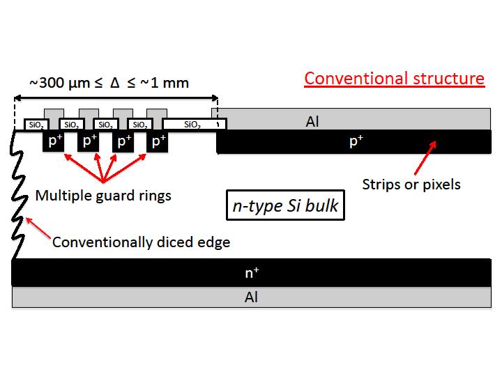
7 Conventional vs. Edgeless 500 µm 50 µm

8 Stop ring functionality Effect of grounding the stop ring n + stop ring V bias p + stop ring 12 th iworid, Cambridge - July 14 th, 2010 V bias
 TOTEM strip")
 Circular test")


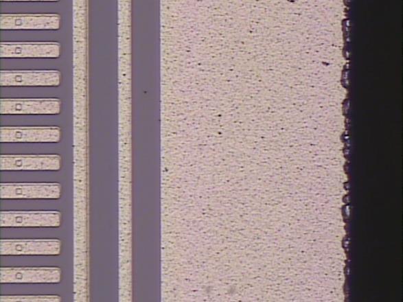
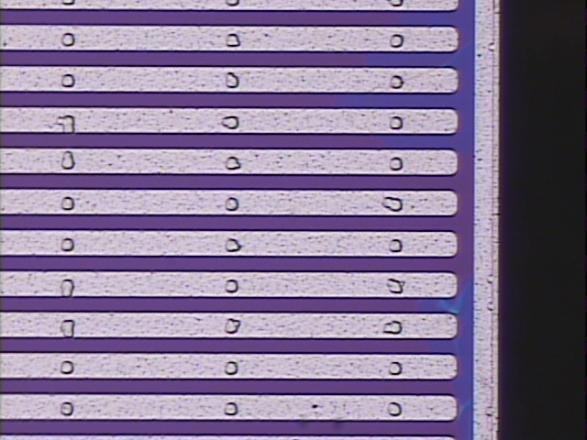
9 Fabrication by Canberra Samples Medipix pixel sensors (10 30 µm edge distance) TOTEM strip sensors (30 µm and 50 µm edge distance) Rectangular test diodes ( µm edge distance) Circular test diodes ( µm edge distance) DRIE dicing and phosphorus diffusion by IMEC Characterization by Nikhef Medipix sensor TOTEM strip sensor Rectangular diode Circular diode 12 th iworid, Cambridge - July 14 th, 2010
10 Humidity No significant dependence on humidity level (except for severely damaged structures)
11 Temperature Normal temperature dependence of thermal generation current
12 J V curves T = K R.H. = % V dep 25 V (from J-V fits) N d (substrate) cm -3 (from resistivity) V fd (V) J 50V (na/cm 2 ) J 50V (na/cm 2 ) Conv Edgeless At 50 V reverse bias, current density levels are: na/cm 2 for p + stop ring structures; na/cm 2 for n + stop ring structures; having a 50 µm edge distance (one pixel column). Breakdown at ( ) V
13 C V curves T = 295 K; R.H. = 30 % f = 100 khz; V AC = 30 mv RMS V dep V (from C-V curves) N d (substrate) (5 7) cm -3 (1/C 2 -V curves) At V dep the capacitance is approx. 10 pf

14 Proof-of-principle Edgeless vs. Conventional

15 J V measurements Inverse correlation: Edge distance and stop ring width current density Structures with a 50 µm edge distance and a 15µm wide stop ring show acceptable current densities at 50 V reverse bias.

16 300 µm edge dist. and 25 µm SR C V curve effects 13 µm edge dist. and 5 µm SR
17 Charges at Si/SiO 2 interface charges/cm 3 at the Si/SiO 2 interface TCAD simulation 12 th iworid, Cambridge - July 14 th, 2010
18 Summary Integrity checks: No significant influence of humidity and normal temperature dependence. Depletion voltage is approximately 25 V; Breakdown at ( ) V reverse bias; The edgeless and conventionally processed devices show comparable current densities. The p+ stop ring structures show lower current densities than the n+ stop ring ones: na/cm 2 for p + stop ring structures; na/cm 2 for n + stop ring structures; with 50 um edge distance, at 50 V reverse bias. Inverse correlation between leakage-current density and both edge distance and stop ring width: Structures with a 50 µm edge distance and a 15 µm wide stop ring show acceptable current-density values. 12 th iworid, Cambridge - July 14 th, 2010

19 What s next? Edge effects in CdTe-based (high-z) sensors. Examination of other dicing techniques (e.g. stealth dicing) Blade diced Stealth diced 12 th iworid, Cambridge - July 14 th, 2010


20 Acknowledgements Canberra: P. Burger, O. Evrard Imec: P. De Moor, K. De Munck, D. S. Tezcan Nikhef: J.L. Visschers, J. Visser 12 th iworid, Cambridge - July 14 th, 2010
21 Back-up slides 12 th iworid, Cambridge - July 14 th, 2010

22 12 th iworid, Cambridge - July 14 th, 2010


23 Dicing Blade dicing Deep Reactive Ion Etching
24 Humidity Severely damaged edge No significant dependence on humidity level (except for severely damaged structures)
25 Integrity checks Temperature
![J V curve fits V V V V FD FD : : I A V BV C leak I A V BV C leak FD A [na/( Vcm 2 )] B [na/(vcm 2 )] C [na/cm 2 ]](/docs-images/78/78445190/images/26-0.jpg "V fd (V) J gen @ 50V (na/cm 2 ) J surf @ 50V (na/cm 2 ) Conv. 0.80 0.03 22 26 4.1 1.5 Edgeless 10 1.4-1.")
26 J V curve fits V V V V FD FD : : I A V BV C leak I A V BV C leak FD A [na/( Vcm 2 )] B [na/(vcm 2 )] C [na/cm 2 ] V fd (V) J 50V (na/cm 2 ) J 50V (na/cm 2 ) Conv Edgeless
27 Electrostatic potential p + stop ring 5 µm SR; 10 µm edge dist. 50 µm SR; 100 µm edge dist SR floating SR biased


28 Stop ring functionality No stop ring 50 µm wide stop ring Hole-current density (changing parameter: electron and hole recombination velocity at the edge)
Silicon Detectors in High Energy Physics
 Thomas Bergauer (HEPHY Vienna) IPM Teheran 22 May 2011 Sunday: Schedule Silicon Detectors in Semiconductor Basics (45 ) Detector concepts: Pixels and Strips (45 ) Coffee Break Strip Detector Performance
Semiconductor Detectors
 Semiconductor Detectors Summary of Last Lecture Band structure in Solids: Conduction band Conduction band thermal conductivity: E g > 5 ev Valence band Insulator Charge carrier in conductor: e - Charge
X-ray induced radiation damage in segmented p + n silicon sensors
 in segmented p + n silicon sensors Jiaguo Zhang, Eckhart Fretwurst, Robert Klanner, Joern Schwandt Hamburg University, Germany E-mail: jiaguo.zhang@desy.de Deutsches Elektronen-Synchrotron (DESY), Germany
A t XFEL experiment, sensors should have. Capacitance calculations in p + n silicon pixel sensors using three dimensional TCAD simulation approach
 Capacitance calculations in p + n silicon pixel sensors using three dimensional TCAD simulation approach Ajay K. Srivastava a,1 E. Fretwurst a, R.Klanner a a Institute for Experimental Physics, University
Development of High-Z Semiconductor Detectors and Their Applications to X-ray/gamma-ray Astronomy
 Development of High-Z Semiconductor Detectors and Their Applications to X-ray/gamma-ray Astronomy Taka Tanaka (SLAC/KIPAC) 9/19/2007 SLAC Advanced Instrumentation Seminar Outline Introduction CdTe Diode
Schottky Rectifiers Zheng Yang (ERF 3017,
 ECE442 Power Semiconductor Devices and Integrated Circuits Schottky Rectifiers Zheng Yang (ERF 3017, email: yangzhen@uic.edu) Power Schottky Rectifier Structure 2 Metal-Semiconductor Contact The work function
EE C245 ME C218 Introduction to MEMS Design Fall 2007
 EE C245 ME C218 Introduction to MEMS Design Fall 2007 Prof. Clark T.-C. Nguyen Dept. of Electrical Engineering & Computer Sciences University of California at Berkeley Berkeley, CA 94720 Lecture 11: Bulk
Challenges for Silicon Pixel Sensors at the XFEL. Table of Content
 Challenges for Silicon Pixel Sensors at the XFEL R.Klanner (Inst. Experimental Physics, Hamburg University) work by J.Becker, E.Fretwurst, I.Pintilie, T.Pöhlsen, J.Schwandt, J.Zhang Table of Content 1.Introduction:
The Hermes Recoil Silicon Detector
 The Hermes Recoil Silicon Detector Introduction Detector design considerations Silicon detector overview TIGRE microstrip sensors Readout electronics Test beam results Vertex 2002 J. Stewart DESY Zeuthen
Simulation of Radiation Effects on Semiconductors
 Simulation of Radiation Effects on Semiconductors Design of Low Gain Avalanche Detectors Dr. David Flores (IMB-CNM-CSIC) Barcelona, Spain david.flores@imb-cnm.csic.es Outline q General Considerations Background
Session 6: Solid State Physics. Diode
 Session 6: Solid State Physics Diode 1 Outline A B C D E F G H I J 2 Definitions / Assumptions Homojunction: the junction is between two regions of the same material Heterojunction: the junction is between
OPTI510R: Photonics. Khanh Kieu College of Optical Sciences, University of Arizona Meinel building R.626
 OPTI510R: Photonics Khanh Kieu College of Optical Sciences, University of Arizona kkieu@optics.arizona.edu Meinel building R.626 Announcements Homework #6 is assigned, due May 1 st Final exam May 8, 10:30-12:30pm
Lecture 2. Introduction to semiconductors Structures and characteristics in semiconductors
 Lecture 2 Introduction to semiconductors Structures and characteristics in semiconductors Semiconductor p-n junction Metal Oxide Silicon structure Semiconductor contact Literature Glen F. Knoll, Radiation
Characterization of 3D thermal neutron semiconductor detectors
 Characterization of 3D thermal neutron semiconductor detectors J.Uher 1, C.Fröjdh 2, J.Jakůbek 1, C.Kenney 3, Z.Kohout 4, V.Linhart 1, S.Parker 5, S.Petersson 2, S.Pospíšil 1, G.Thungström 2 (1),, Czech
Status Report: Charge Cloud Explosion
 Status Report: Charge Cloud Explosion J. Becker, D. Eckstein, R. Klanner, G. Steinbrück University of Hamburg Detector laboratory 1. Introduction and Motivation. Set-up available for measurement 3. Measurements
Lecture 2. Introduction to semiconductors Structures and characteristics in semiconductors
 Lecture 2 Introduction to semiconductors Structures and characteristics in semiconductors Semiconductor p-n junction Metal Oxide Silicon structure Semiconductor contact Literature Glen F. Knoll, Radiation
Midterm I - Solutions
 UNIVERSITY OF CALIFORNIA College of Engineering Department of Electrical Engineering and Computer Sciences EECS 130 Spring 2008 Professor Chenming Hu Midterm I - Solutions Name: SID: Grad/Undergrad: Closed
Simulation results from double-sided and standard 3D detectors
 Simulation results from double-sided and standard 3D detectors David Pennicard, University of Glasgow Celeste Fleta, Chris Parkes, Richard Bates University of Glasgow G. Pellegrini, M. Lozano - CNM, Barcelona
Guard Ring Width Impact on Impact Parameter Performances and Structure Simulations
 LHCb-2003-034, VELO Note 13th May 2003 Guard Ring Width Impact on Impact Parameter Performances and Structure Simulations authors A Gouldwell, C Parkes, M Rahman, R Bates, M Wemyss, G Murphy The University
Device 3D. 3D Device Simulator. Nano Scale Devices. Fin FET
 Device 3D 3D Device Simulator Device 3D is a physics based 3D device simulator for any device type and includes material properties for the commonly used semiconductor materials in use today. The physical
Impact of high photon densities on AGIPD requirements
 Impact of high photon densities on AGIPD requirements Julian Becker University of Hamburg Detector Laboratory new data 1. Heating estimations 2. Confined breakdown 3. Range switching in adjacent pixels
Junction Diodes. Tim Sumner, Imperial College, Rm: 1009, x /18/2006
 Junction Diodes Most elementary solid state junction electronic devices. They conduct in one direction (almost correct). Useful when one converts from AC to DC (rectifier). But today diodes have a wide
Status Report: Multi-Channel TCT
 Status Report: Multi-Channel TCT J. Becker, D. Eckstein, R. Klanner, G. Steinbrück University of Hamburg 1. Introduction 2. Set-up and measurement techniques 3. First results from single-channel measurements
Impact of high photon densities on AGIPD requirements
 Impact of high photon densities on AGIPD requirements Julian Becker University of Hamburg Detector Laboratory 1. Si-type influence on charge collection time 2. Measurements on charge collection time 3.
Final Examination EE 130 December 16, 1997 Time allotted: 180 minutes
 Final Examination EE 130 December 16, 1997 Time allotted: 180 minutes Problem 1: Semiconductor Fundamentals [30 points] A uniformly doped silicon sample of length 100µm and cross-sectional area 100µm 2
Chapter 7. The pn Junction
 Chapter 7 The pn Junction Chapter 7 PN Junction PN junction can be fabricated by implanting or diffusing donors into a P-type substrate such that a layer of semiconductor is converted into N type. Converting
Lecture 2. Introduction to semiconductors Structures and characteristics in semiconductors. Fabrication of semiconductor sensor
 Lecture 2 Introduction to semiconductors Structures and characteristics in semiconductors Semiconductor p-n junction Metal Oxide Silicon structure Semiconductor contact Fabrication of semiconductor sensor
1) CMOS-Sensors for vertex-detectors 2) CMOS-Sensors for X-ray imaging 3) Sensor with a 3-T-preamplifier 4) Sensor with nearly full depletion
 CMOS-Sensors for vertex-detectors 2) CMOS-Sensors for X-ray imaging 3) Sensor with a 3-T-preamplifier 4) Sensor with nearly full depletion") AD vanced MO nolithic ensors for S CMOS-sensors for energy-resolved X-ray imaging Dennis Doering, Samir Amar, Jerome Baudot², Michael Deveaux, Wojciech Dulinski², Maciej Kachel², Tomasz Hemperek³, Christian
AD vanced MO nolithic ensors for S CMOS-sensors for energy-resolved X-ray imaging Dennis Doering, Samir Amar, Jerome Baudot², Michael Deveaux, Wojciech Dulinski², Maciej Kachel², Tomasz Hemperek³, Christian
Silicon Detectors. Particle Physics
 Mitglied der Helmholtz-Gemeinschaft Silicon Detectors for Particle Physics 9. August 2012 Ralf Schleichert, Institut für Kernphysik Outline Different Cameras Silicon Detectors Taking Pictures in Particle
Semiconductor-Detectors
 Semiconductor-Detectors 1 Motivation ~ 195: Discovery that pn-- junctions can be used to detect particles. Semiconductor detectors used for energy measurements ( Germanium) Since ~ 3 years: Semiconductor
Development of Radiation Hard Si Detectors
 Development of Radiation Hard Si Detectors Dr. Ajay K. Srivastava On behalf of Detector Laboratory of the Institute for Experimental Physics University of Hamburg, D-22761, Germany. Ajay K. Srivastava
Lecture 8. Detectors for Ionizing Particles
 Lecture 8 Detectors for Ionizing Particles Content Introduction Overview of detector systems Sources of radiation Radioactive decay Cosmic Radiation Accelerators Interaction of Radiation with Matter General
SILICON PARTICLE DETECTOR
 SILICON PARTICLE DETECTOR Supervised Learning Project Eslikumar Adiandhra 12D260012 Department of Physics, IIT Bombay Guide: Prof. Raghava Varma Department of Physics, IIT Bombay November 8, 2015 Abstract
NEW X-RAY DETECTORS FOR XRF ANALYSIS. Jan S. Iwanczyk & Bradley E. Patt Photon Imaging, Inc., Northridge, CA 91324
 951 NEW X-RAY DETECTORS FOR XRF ANALYSIS Jan S. Iwanczyk & Bradley E. Patt Photon Imaging, Inc., Northridge, CA 91324 Abstract The use of miniaturized XRF instrumentation for in-vivo applications imposes
Dark Current Limiting Mechanisms in CMOS Image Sensors
 Dark Current Limiting Mechanisms in CMOS Image Sensors Dan McGrath BAE Systems Information and Electronic Systems Integration Inc., Lexington, MA 02421, USA,
CTU Prague RD50 Group
 CTU Prague RD50 Group Detector structures on GaAs (Mesa with Guard Rings) T. Horazdovský, D. Chren, Z. Kohout, M. Solar, B. Sopko ME CTU V. Jurka, E. Hulicius IP ASCR S. Pospisil IEAP CTU Contents Motivation
Efficient electron transport on helium with silicon integrated circuits
 Efficient electron transport on helium with silicon integrated circuits - - + - - Forrest Bradbury 1 and Maika Takita 1, Kevin Eng 2, Tom M Gurrieri 2, Kathy J Wilkel 2, Stephen A Lyon 1 1 Princeton University
Mara Bruzzi INFN and University of Florence, Italy and SCIPP, UC Santa Cruz, USA
 SCIPP 06/16 September 2006 Capacitance-Voltage analysis at different temperatures in heavily irradiated silicon detectors Mara Bruzzi INFN and University of Florence, Italy and SCIPP, UC Santa Cruz, USA
physics/ Sep 1997
 GLAS-PPE/97-6 28 August 1997 Department of Physics & Astronomy Experimental Particle Physics Group Kelvin Building, University of Glasgow, Glasgow, G12 8QQ, Scotland. Telephone: +44 - ()141 3398855 Fax:
Energetic particles and their detection in situ (particle detectors) Part II. George Gloeckler
 Part II. George Gloeckler") Energetic particles and their detection in situ (particle detectors) Part II George Gloeckler University of Michigan, Ann Arbor, MI University of Maryland, College Park, MD Simple particle detectors Gas-filled
Energetic particles and their detection in situ (particle detectors) Part II George Gloeckler University of Michigan, Ann Arbor, MI University of Maryland, College Park, MD Simple particle detectors Gas-filled
Components of a generic collider detector
 Lecture 24 Components of a generic collider detector electrons - ionization + bremsstrahlung photons - pair production in high Z material charged hadrons - ionization + shower of secondary interactions
Lecture 18. New gas detectors Solid state trackers
 Lecture 18 New gas detectors Solid state trackers Time projection Chamber Full 3-D track reconstruction x-y from wires and segmented cathode of MWPC z from drift time de/dx information (extra) Drift over
ECE-342 Test 2 Solutions, Nov 4, :00-8:00pm, Closed Book (one page of notes allowed)
") ECE-342 Test 2 Solutions, Nov 4, 2008 6:00-8:00pm, Closed Book (one page of notes allowed) Please use the following physical constants in your calculations: Boltzmann s Constant: Electron Charge: Free
ECE-342 Test 2 Solutions, Nov 4, 2008 6:00-8:00pm, Closed Book (one page of notes allowed) Please use the following physical constants in your calculations: Boltzmann s Constant: Electron Charge: Free
Development and characterization of 3D semiconductor X-rays detectors for medical imaging
 Development and characterization of 3D semiconductor X-rays detectors for medical imaging Marie-Laure Avenel, Eric Gros d Aillon CEA-LETI, DETectors Laboratory marie-laure.avenel@cea.fr Outlines Problematic
Segmented 1.55um Laser with 400% Differential Quantum Efficiency J. Getty, E. Skogen, L. Coldren, University of California, Santa Barbara, CA.
 Segmented 1.55um Laser with 400% Differential Quantum Efficiency J. Getty, E. Skogen, L. Coldren, University of California, Santa Barbara, CA. Abstract: By electrically segmenting, and series-connecting
UNIVERSITY OF CALIFORNIA College of Engineering Department of Electrical Engineering and Computer Sciences. EECS 130 Professor Ali Javey Fall 2006
 UNIVERSITY OF CALIFORNIA College of Engineering Department of Electrical Engineering and Computer Sciences EECS 130 Professor Ali Javey Fall 2006 Midterm 2 Name: SID: Closed book. Two sheets of notes are
FYS3410 Condensed matter physics
 FYS3410 Condensed matter physics Lecture 23 and 24: pn-junctions and electrooptics Randi Haakenaasen UniK/UiO Forsvarets forskningsinstitutt 11.05.2016 and 18.05.2016 Outline Why pn-junctions are important
Solid State Detectors Semiconductor detectors Halbleiterdetektoren
 Solid State Detectors Semiconductor detectors Halbleiterdetektoren Doris Eckstein DESY Where are solid state detectors used? > Nuclear Physics: Energy measurement of charged particles (particles up to
Regents of the University of California
 Deep Reactive-Ion Etching (DRIE) DRIE Issues: Etch Rate Variance The Bosch process: Inductively-coupled plasma Etch Rate: 1.5-4 μm/min Two main cycles in the etch: Etch cycle (5-15 s): SF 6 (SF x+ ) etches
LAYOUT TECHNIQUES. Dr. Ivan Grech
 LAYOUT TECHNIQUES OUTLINE Transistor Layout Resistor Layout Capacitor Layout Floor planning Mixed A/D Layout Automatic Analog Layout Layout Techniques Main Layers in a typical Double-Poly, Double-Metal
Fabrication of a 600V/20A 4H-SiC Schottky Barrier Diode
 Fabrication of a 600V/20A 4H-SiC Schottky Barrier Diode In-Ho Kang, Sang-Cheol Kim, Jung-Hyeon Moon, Wook Bahng, and Nam-Kyun Kim Power Ssemiconductor Research Center, Korea Electrotechnology Research
Lecture #27. The Short Channel Effect (SCE)
") Lecture #27 ANNOUNCEMENTS Design Project: Your BJT design should meet the performance specifications to within 10% at both 300K and 360K. ( β dc > 45, f T > 18 GHz, V A > 9 V and V punchthrough > 9 V )
Lecture #27 ANNOUNCEMENTS Design Project: Your BJT design should meet the performance specifications to within 10% at both 300K and 360K. ( β dc > 45, f T > 18 GHz, V A > 9 V and V punchthrough > 9 V )
Fundamentals of ANALOG TO DIGITAL CONVERTERS: Part I.3. Technology
 Fundamentals of ANALOG TO DIGITAL CONVERTERS: Part I.3 Technology January 019 Texas A&M University 1 Spring, 019 Well-Diffusion Resistor Example shows two long resistors for K range Alternatively, serpentine
A study of silicon sensor for ILD ECAL
 A study of silicon sensor for ILD ECAL arxiv:1403.7953v1 [physics.ins-det] 31 Mar 2014 Tatsuhiko Tomita Shion Chen, Daniel Jeans, Yoshio Kamiya, Kiyotomo Kawagoe, Sachio Komamiya, Chihiro Kozakai, Yohei
EECS130 Integrated Circuit Devices
 EECS130 Integrated Circuit Devices Professor Ali Javey 9/18/2007 P Junctions Lecture 1 Reading: Chapter 5 Announcements For THIS WEEK OLY, Prof. Javey's office hours will be held on Tuesday, Sept 18 3:30-4:30
The Silicon-Tungsten Tracker of the DAMPE Mission
 The Silicon-Tungsten Tracker of the DAMPE Mission Philipp Azzarello, DPNC, University of Geneva for the DAMPE-STK collaboration 10th International Hiroshima Symposium on the Development and Application
The path to Germanium Drift Detectors
 The path to Germanium Drift Detectors A. Castoldi, C. Guazzoni, S. Maffessanti Politecnico di Milano and INFN Milano, Italy T. Krings Forschungszentrum Jülich, IKP, Jülich, Germany IFDEPS 2018, Annecy,
Characteristics of Neutral Beam Generated by a Low Angle Reflection and Its Etch Characteristics by Halogen-Based Gases
 Characteristics of Neutral Beam Generated by a Low Angle Reflection and Its Etch Characteristics by Halogen-Based Gases Geun-Young Yeom SungKyunKwan University Problems of Current Etch Technology Scaling
Supplementary Figure S1. AFM images of GraNRs grown with standard growth process. Each of these pictures show GraNRs prepared independently,
 Supplementary Figure S1. AFM images of GraNRs grown with standard growth process. Each of these pictures show GraNRs prepared independently, suggesting that the results is reproducible. Supplementary Figure
Semiconductor X-Ray Detectors. Tobias Eggert Ketek GmbH
 Semiconductor X-Ray Detectors Tobias Eggert Ketek GmbH Semiconductor X-Ray Detectors Part A Principles of Semiconductor Detectors 1. Basic Principles 2. Typical Applications 3. Planar Technology 4. Read-out
Outline. Introduction, motivation Readout electronics, Peltier cooling Input J-FETsJ
 Progress in low energy X-rayX spectroscopy using semi-insulating insulating GaAs detectors F. Dubecký 1, B. Zaťko 1, P. Boháček 1, L. Ryć 2, E. Gombia 2, and V. Nečas 3 1 IEE SAS, Bratislava, Slovakia
Energy calibration of the threshold of Medipix for ATLAS
 Energy calibration of the threshold of Medipix for ATLAS Céline Lebel Université de Montréal lebel@lps.umontreal.ca presenting for the Institut of Experimental and Applied Physics of the Czech Technical
Epitaxial SiC Schottky barriers for radiation and particle detection
 Epitaxial SiC Schottky barriers for radiation and particle detection M. Bruzzi, M. Bucciolini, R. D'Alessandro, S. Lagomarsino, S. Pini, S. Sciortino INFN Firenze - Università di Firenze F. Nava INFN Bologna
Mass Determination of Rn and Hg isotopes using MASHA
 Mass Determination of Rn and Hg isotopes using MASHA Alfred M. Sehone Lumkile Msebi Oleg Lishyk Stanislav Stanishevski Yuliya Brechko Supervisor Krupa Lubosh Flerov Laboratory of Nuclear reactions, JINR,
Tracking in High Energy Physics: Silicon Devices!
 Tracking in High Energy Physics: Silicon Devices! G. Leibenguth XIX Graduiertenkolleg Heidelberg 11-12. October 2007 Content Part 1: Basics on semi-conductor Part 2: Construction Part 3: Two Examples Part
Basic Physics of Semiconductors
 Basic Physics of Semiconductors Semiconductor materials and their properties PN-junction diodes Reverse Breakdown EEM 205 Electronics I Dicle University, EEE Dr. Mehmet Siraç ÖZERDEM Semiconductor Physics
Lecture 16: Circuit Pitfalls
 Introduction to CMOS VLSI Design Lecture 16: Circuit Pitfalls David Harris Harvey Mudd College Spring 2004 Outline Pitfalls Detective puzzle Given circuit and symptom, diagnose cause and recommend solution
3D Sensor Measurements at Univ. New Mexico
 3D Sensor Measurements at Univ. New Mexico Martin Hoeferkamp 10 Nov 2005 Introduction Framework: to assist ATLAS in selecting a technology for pixel sensors in the upgrade era. Specifically: to evaluate
Solid State Detectors
 Solid State Detectors Most material is taken from lectures by Michael Moll/CERN and Daniela Bortoletto/Purdue and the book Semiconductor Radiation Detectors by Gerhard Lutz. In gaseous detectors, a charged
Radiation hardness of Low Gain Amplification Detectors (LGAD)
") Radiation hardness of Low Gain Amplification Detectors (LGAD) G. Kramberger, V. Cindro, I. Mandić, M. Mikuž Ϯ, M. Zavrtanik Jožef Stefan Institute, Ljubljana, Slovenia Ϯ also University of Ljubljana, Faculty
Radiation hardness of Low Gain Amplification Detectors (LGAD) G. Kramberger, V. Cindro, I. Mandić, M. Mikuž Ϯ, M. Zavrtanik Jožef Stefan Institute, Ljubljana, Slovenia Ϯ also University of Ljubljana, Faculty
CVD Diamond History Introduction to DDL Properties of Diamond DDL Proprietary Contact Technology Detector Applications BDD Sensors
 Diamond Detectors CVD Diamond History Introduction to DDL Properties of Diamond DDL Proprietary Contact Technology Detector Applications BDD Sensors Kevin Oliver CEO Alex Brown Sales & Marketing 20 May,
GaAs X- Ray System Detectors for Medical Applications
 GaAs X- Ray System Detectors for Medical Applications MARIA RIZZI, MICHELE MAURANTONIO, BENIAMINO CASTAGNOLO Dipartimento di Elettrotecnica ed Elettronica, Politecnico di Bari v. E. Orabona, 4-7125 Bari
DEPFET sensors development for the Pixel Detector of BELLE II
 DEPFET sensors development for the Pixel Detector of BELLE II 13 th Topical Seminar on Innovative Particle and Radiation Detectors (IPRD13) 7 10 October 2013, Siena, Italy Paola Avella for the DEPFET collaboration
Supplementary Information
 Supplementary Information Supplementary Figure 1 Raman spectroscopy of CVD graphene on SiO 2 /Si substrate. Integrated Raman intensity maps of D, G, 2D peaks, scanned across the same graphene area. Scale
LEC E T C U T R U E R E 17 -Photodetectors
 LECTURE 17 -Photodetectors Topics to be covered Photodetectors PIN photodiode Avalanche Photodiode Photodetectors Principle of the p-n junction Photodiode A generic photodiode. Photodetectors Principle
Development of high-z sensors for pixel array detectors
 Development of high-z sensors for pixel array detectors David Pennicard, DESY Heinz Graafsma, Sabine Sengelmann, Sergej Smoljanin, Helmut Hirsemann, Peter Goettlicher Vertex 2010, Loch Lomond, 6-11 June
Control of the fabrication process for the sensors of the CMS Silicon Strip Tracker. Anna Macchiolo. CMS Collaboration
 Control of the fabrication process for the sensors of the CMS Silicon Strip Tracker Anna Macchiolo Universita di Firenze- INFN Firenze on behalf of the CMS Collaboration 6 th International Conference on
EE C245 ME C218 Introduction to MEMS Design Fall 2007
 EE C245 ME C218 Introduction to MEMS Design Fall 2007 Prof. Clark T.-C. Nguyen Dept. of Electrical Engineering & Computer Sciences University of California at Berkeley Berkeley, CA 94720 Lecture 12: Mechanics
Application Note. The Continuous Air Monitoring (CAM) PIPS Detector Properties and Applications
 PIPS Detector Properties and Applications") Application Note The Continuous Air Monitoring (CAM) PIPS Detector Properties and Applications Introduction The increasing demand for safety in nuclear installations calls for continuous survey of airborne
Application Note The Continuous Air Monitoring (CAM) PIPS Detector Properties and Applications Introduction The increasing demand for safety in nuclear installations calls for continuous survey of airborne
First Sensor APD Array Data Sheet Part Description 64AA SMD Order #
 Responsivity (A/W) First Sensor APD Array Data Sheet Features Description Application RoHS 64 element APD array High QE >8% for λ = 7-91 nm High speed, low noise High uniformity, low cross talk Absolute
Purpose: To convert the received optical signal into an electrical lsignal.
 OPTICAL DETECTORS Optical Detectors Purpose: To convert the received optical signal into an electrical lsignal. Requirements For Detector HIGH SENSITIVITY (at operating wave lengths) at normal op. temp
High-Resolution Gamma-Ray and Neutron Detectors For Nuclear Spectroscopy
 High-Resolution Gamma-Ray and Neutron Detectors For Nuclear Spectroscopy Thomas Niedermayr, I. D. Hau, S. Terracol, T. Miyazaki, S. E. Labov and S. Friedrich Former colleagues: M. F. Cunningham, J. N.
Guard Ring Simulations for n-on-p Silicon Particle Detectors
 Physics Physics Research Publications Purdue University Year 2010 Guard Ring Simulations for n-on-p Silicon Particle Detectors O. Koybasi G. Bolla D. Bortoletto This paper is posted at Purdue e-pubs. http://docs.lib.purdue.edu/physics
MOS Transistor Properties Review
 MOS Transistor Properties Review 1 VLSI Chip Manufacturing Process Photolithography: transfer of mask patterns to the chip Diffusion or ion implantation: selective doping of Si substrate Oxidation: SiO
Novel Back-Biased UTBB Lateral SCR for FDSOI ESD Protections
 Novel Back-Biased UTBB Lateral SCR for FDSOI ESD Protections Yohann Solaro 1,2,3, Pascal Fonteneau 1, Charles-Alexandre Legrand 1 Claire Fenouillet-Beranger 1,3, Philippe Ferrari 2, Sorin Cristoloveanu
Package Lead Code Identification SINGLE 3 SERIES 3 UNCONNECTED PAIR RING QUAD
 Surface Mount RF Schottky Barrier Diodes Technical Data HSMS-28XX Series Features Surface Mount SOT-2/SOT- 4 Package Low Turn-On Voltage (As Low as 4 V at ma) Low FIT (Failure in Time) Rate* Six-sigma
6.012 Electronic Devices and Circuits
 Page 1 of 1 YOUR NAME Department of Electrical Engineering and Computer Science Massachusetts Institute of Technology 6.12 Electronic Devices and Circuits Exam No. 1 Wednesday, October 7, 29 7:3 to 9:3
Development of a Radiation Hard CMOS Monolithic Pixel Sensor
 Development of a Radiation Hard CMOS Monolithic Pixel Sensor M. Battaglia 1,2, D. Bisello 3, D. Contarato 2, P. Denes 2, D. Doering 2, P. Giubilato 2,3, T.S. Kim 2, Z. Lee 2, S. Mattiazzo 3, V. Radmilovic
X-ray Radiation Damage in P-N Junction Diode
 X-ray Radiation Damage in P-N Junction Diode Itsara Srithanachai 1, Surada Ueamanapong 1, Yuwadee Sundarasaradula 1, Amporn Poyai 2, Surasak Niemcharoen 1 1 Department of Electronics, Faculty of Engineering,
Maria-Alexandra PAUN, PhD
 On the modelisation of the main characteristics of SOI Hall cells by three-dimensional physical simulations Maria-Alexandra PAUN, PhD Visiting Researcher High Voltage Microelectronics and Sensors (HVMS)
Ranjeet Dalal, Ashutosh Bhardwaj, Kirti Ranjan, Kavita Lalwani and Geetika Jain
 Simulation of Irradiated Si Detectors, Ashutosh Bhardwaj, Kirti Ranjan, Kavita Lalwani and Geetika Jain CDRST, Department of physics and Astrophysics, University of Delhi, India E-mail: rdalal@cern.ch
Package Lead Code Identification SINGLE 3 SERIES 3 UNCONNECTED PAIR RING QUAD
 Surface Mount RF Schottky Barrier Diodes Technical Data HSMS-28XX Series Features Surface Mount SOT-2/SOT- 4 Package Low Turn-On Voltage (As Low as 4 V at ma) Low FIT (Failure in Time) Rate* Six-sigma
Study of Edgeless TimePix Pixel Devices. Dylan Hsu Syracuse University 4/30/2014
 Study of Edgeless TimePix Pixel Devices Dylan Syracuse University 2 3 Million-Dollar Question Universe is made of matter Particle decays putatively produce equal amounts of matter and antimatter Where
Modelling of Diamond Devices with TCAD Tools
 RADFAC Day - 26 March 2015 Modelling of Diamond Devices with TCAD Tools A. Morozzi (1,2), D. Passeri (1,2), L. Servoli (2), K. Kanxheri (2), S. Lagomarsino (3), S. Sciortino (3) (1) Engineering Department
Silicon Drift Detectors for gamma-ray detection: 15 years of research (and collaboration between Politecnico and INAF-Milano)
") Silicon Drift Detectors for gamma-ray detection: 15 years of research (and collaboration between Politecnico and INAF-Milano) Outline The Silicon Drift Detector (SDD) Gamma-ray detectors based on scintillators
Silicon Drift Detectors for gamma-ray detection: 15 years of research (and collaboration between Politecnico and INAF-Milano) Outline The Silicon Drift Detector (SDD) Gamma-ray detectors based on scintillators
Photodiodes and other semiconductor devices
 Photodiodes and other semiconductor devices Chem 243 Winter 2017 What is a semiconductor? no e - Empty e levels Conduction Band a few e - Empty e levels Filled e levels Filled e levels lots of e - Empty
D. Meier. representing the RD42 Collaboration. Bristol University, CERN, CPP Marseille, Lawrence Livermore National Lab, LEPSI
 Diamond as a Particle Detector D. Meier representing the RD42 Collaboration Bristol University, CERN, CPP Marseille, Lawrence Livermore National Lab, LEPSI Strasbourg, Los Alamos National Lab, MPIK Heidelberg,
MEGAWATT SOLID-STATE ELECTRONICS
 MATERIALS, PROCESS AND DEVICE DEVELOPMENT FOR GaN (and SiC) POWER DEVICES University of Florida: SRI: MCNC: Device Design/Simulation (In Collaboration with Sandia) Process Development Device Fabrication
Radiation damage models: comparison between Silvaco and Synopsys
 Radiation damage models: comparison between Silvaco and Synopsys J. Beyer a), M. Bomben b), A. Macchiolo a), R. Nisius a) a) Max Planck Institut für Physik, München b) LPNHE & Université Paris Diderot,
CMOS Devices. PN junctions and diodes NMOS and PMOS transistors Resistors Capacitors Inductors Bipolar transistors
 CMOS Devices PN junctions and diodes NMOS and PMOS transistors Resistors Capacitors Inductors Bipolar transistors PN Junctions Diffusion causes depletion region D.R. is insulator and establishes barrier