Beyond silicon electronics-fets with nanostructured graphene channels with high on-off ratio and highmobility
|
|
|
- Reginald Nash
- 5 years ago
- Views:
Transcription
1 Beyond silicon electronics-fets with nanostructured graphene channels with high on-off ratio and highmobility M.Dragoman 1, A.Dinescu 1, and D.Dragoman 2 1 National Institute for Research and Development in Microtechnology Str. Erou Iancu Nicolae 126 A, Voluntari, Romania 2 Univ. Bucharest, Physics Faculty, P.O. Box MG-11, Bucharest, Romania mircea.dragoman@imt.ro, adrian.dinescu@imt.ro


2 Research Centre for Integrated Systems Nanotechnologies and Carbon Based Nanomaterialsopened in dec.2015 Graphene oxide/pedot:pss on PET de 40 µm; Equipments for : CVD for growing graphene; ALD; dielectric growth, MBE, metal deposition + Raman and FTIR spectroscopy in a 240 m2 clean room with class 1000, and some areas with class millions Euro investments (UE)


3 My life with graphene Graphene ink- Nanointegris Graphene flakes 4 inch graphene wafer on HR Si Graphene Supermarket 4 inch graphene wafer on HR Si Graphenea,Spaian Towards 6 inch wafer from Manchester Univ. Prof. A. Geim and dr. Peter Blake First CVD graphene grown in IMT Bucharest, january 2016
4 GRAPHENE ELECTRONICS CONUNDRUM : HIGH MOBILITY AND HIGH ON-OFF RATIO Graphene electronics was almost abandoned because the key electronic device the graphene field-effect transistor (GFET), cannot be switched on and off due to the absence of a bandgap. How to solve the conundrum? GFET with a nanopatterned channel is a high-mobility, high on-off ratio FET.

5 SEM image of a nanopatterned GFET channel with 2 µm. E g =0.16 ev nanohole array with a period of 100 nm and a diameter of 20 nm the corresponding bandgap is about 0.16 ev, but this parameter increases to 0.2 ev if the nanohole diameter becomes 30 nm.


-40 % are working")
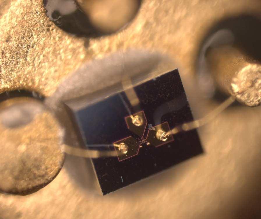
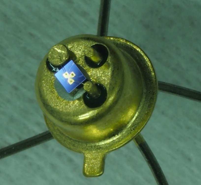
6 D Cr (10nm)/Au (150 nm) Channel length : 1,2,4 8 µm W=2 µm HSQ gate dielectric 40 nm thick 90 GFETs on a graphene chip cut from a 4 inch graphene wafer (CVD growth and transfer Graphenea)-40 % are working very well S 200 nm
 appears at = -3 V and -4 V.")
7 Drain current vs drain voltage characteristics of a nanoperforated GFET at various gate voltages indicated in the inset - the drain current tends to saturate at some gate voltages, e.g. at 1 V and -1 V - a clear negative differential resistance region (NDR) appears at = -3 V and -4 V.
8
9 L = 2 µm I D (ma) E-3 0 V 0.5 V 1 V 1.5 V 2 V L=2 µm 1E-4 µ (cm 2 /Vs) E V G (V ) I on /I off L (µm) Mobility the on/off ratio between drain currents at 0 V and 2 V as a function L (µm) of the channel length for several gate voltages indicated in the inset. on/off
10 V -0.5 V 0 V 0.5 V 1 V L loc (µm) 2.0 g D (ms) V -0.5 V 0.5 V V D (V) g D L (µm) ( L) = g d 0 exp( L / Lloc Strong localization L loc =1.9µm ) Long room temperature localization and phase coherence lengths (8 µm) could be explained by the nonuniform nanohole diameters in the transverse direction, which induces charge carrier focusing/guiding along the middle part of the channel such that the charge carriers avoid the boundaries of the channels and the associated strong recombination centers. These non-uniformities in the hole diameters are induced by the proximity effects due to e-beam lithography. For a nanohole array with a period of 100 nm and a diameter of 20 nm the corresponding bandgap is about 0.16 ev, but this parameter increases to 0.2 ev if the nanohole diameter becomes 30 nm. As a result, the charge carriers are guided through the central part of the channel and recombinations at channel boundaries are strongly reduced.

11 Thank you! Romanian Research Centre for Carbon Based Nanomaterials Electronics at atomic scale.
ROOM TEMPERATURE NANOSTRUCTURED GRAPHENE TRANSISTOR WITH HIGH ON/OFF RATIO Bucharest, Romania,
 1 ROOM TEMPERATURE NANOSTRUCTURE GRAPHENE TRANSISTOR WITH HIGH ON/OFF RATIO Mircea ragoman 1*, Adrian inescu 1, and aniela ragoman 2,3 1 National Institute for Research and evelopment in Microtechnology
Ph.D. students, postdocs, and young researchers, which need to absorb a lot of new knowledge, not taught at universities, in a rather short time.
 We have started to work in the area of graphene at the end of 2006, discovering that the fascinating Dirac equations could drive to new discoveries in solid-state physics. At that time, although the Dirac
Supporting Online Material for
 www.sciencemag.org/cgi/content/full/327/5966/662/dc Supporting Online Material for 00-GHz Transistors from Wafer-Scale Epitaxial Graphene Y.-M. Lin,* C. Dimitrakopoulos, K. A. Jenkins, D. B. Farmer, H.-Y.
Scaling up Chemical Vapor Deposition Graphene to 300 mm Si substrates
 Scaling up Chemical Vapor Deposition Graphene to 300 mm Si substrates Co- Authors Aixtron Alex Jouvray Simon Buttress Gavin Dodge Ken Teo The work shown here has received partial funding from the European
NEGATIVE DIFFERENTIAL RESISTANCE IN GRAPHENE-BASED BALLISTIC FIELD-EFFECT-TRANSISTOR WITH OBLIQUE TOP GATE Bucharest, Romania,
 1 NEGATIVE DIFFERENTIAL RESISTANCE IN GRAPHENE-BASED BALLISTIC FIELD-EFFECT-TRANSISTOR WITH OBLIQUE TOP GATE Mircea Dragoman 1*, Adrian Dinescu 1, and Daniela Dragoman 2 1 National Institute for Research
MICROWAVE AND MILLIMETERWAVE ELECTRICAL PERMITTIVITY OF GRAPHENE MONOLAYER. G. Konstantinidis 3
 1 MICROWAVE AND MILLIMETERWAVE ELECTRICAL PERMITTIVITY OF GRAPHENE MONOLAYER Alina Cismaru 1, Mircea Dragoman 1*, Adrian Dinescu 1, Daniela Dragoman 2, G. Stavrinidis, G. Konstantinidis 3 1 National Institute
Supplementary Figure S1. AFM images of GraNRs grown with standard growth process. Each of these pictures show GraNRs prepared independently,
 Supplementary Figure S1. AFM images of GraNRs grown with standard growth process. Each of these pictures show GraNRs prepared independently, suggesting that the results is reproducible. Supplementary Figure
ROOM TEMPERATURE ON-WAFER BALLISTIC GRAPHENE FIELD- EFFECT-TRANSISTOR WITH OBLIQUE DOUBLE-GATE , Bucharest, Romania, Romania
 1 ROOM TEMPERATURE ON-WAFER BALLISTIC GRAPHENE FIELD- EFFECT-TRANSISTOR WITH OBLIQUE DOUBLE-GATE Mircea Dragoman 1*, Adrian Dinescu 1, and Daniela Dragoman 2,3 1 National Institute for Research and Development
Spring Semester 2012 Final Exam
 Spring Semester 2012 Final Exam Note: Show your work, underline results, and always show units. Official exam time: 2.0 hours; an extension of at least 1.0 hour will be granted to anyone. Materials parameters
Direct Measurement of Adhesion Energy of Monolayer Graphene As-Grown. on Copper and Its Application to Renewable Transfer Process
 SUPPORTING INFORMATION Direct Measurement of Adhesion Energy of Monolayer Graphene As-Grown on Copper and Its Application to Renewable Transfer Process Taeshik Yoon 1, Woo Cheol Shin 2, Taek Yong Kim 2,
Nanoscale Diodes Without p-n Junctions
 Nanoscale Diodes Without p-n Junctions Mircea DRAGOMAN National Institute for Research and Development in Microtechnology (IMT), P.O. Box 38-160, 023573 Bucharest, Romania E-mail: mircea.dragoman@imt.ro
Graphene Field Effect Devices Operating in Differential Circuit Configuration
 Graphene Field Effect Devices Operating in Differential Circuit Configuration C. Nyffeler a,*, M.S. Hanay b,c, D. Sacchetto a, Y. Leblebici a a Institute of Electrical Engineering, EPFL, Lausanne, Switzerland
ELECTRONIC DEVICES BASED ON CARBON NANOTUBES AND GRAPHENE
 THE PUBLISHING HOUSE PROCEEDINGS OF THE ROMANIAN ACADEMY, Series A, OF THE ROMANIAN ACADEMY Volume 10, Number 1/2009, pp. 000 000 ELECTRONIC DEVICES BASED ON CARBON NANOTUBES AND GRAPHENE Mircea DRAGOMAN
ECE 342 Electronic Circuits. Lecture 6 MOS Transistors
 ECE 342 Electronic Circuits Lecture 6 MOS Transistors Jose E. Schutt-Aine Electrical & Computer Engineering University of Illinois jesa@illinois.edu 1 NMOS Transistor Typically L = 0.1 to 3 m, W = 0.2
Wafer-scale fabrication of graphene
 Wafer-scale fabrication of graphene Sten Vollebregt, MSc Delft University of Technology, Delft Institute of Mircosystems and Nanotechnology Delft University of Technology Challenge the future Delft University
Electrical Characteristics of Multilayer MoS 2 FET s
 Electrical Characteristics of Multilayer MoS 2 FET s with MoS 2 /Graphene Hetero-Junction Contacts Joon Young Kwak,* Jeonghyun Hwang, Brian Calderon, Hussain Alsalman, Nini Munoz, Brian Schutter, and Michael
Graphene and new 2D materials: Opportunities for High Frequencies applications
 Graphene and new 2D materials: Opportunities for High Frequencies applications April 21th, 2015 H. Happy, E. Pallecchi, B. Plaçais, D. Jiménez, R. Sordan, D. Neumaier Graphene Flagship WP4 HF electronic
TRANSVERSE SPIN TRANSPORT IN GRAPHENE
 International Journal of Modern Physics B Vol. 23, Nos. 12 & 13 (2009) 2641 2646 World Scientific Publishing Company TRANSVERSE SPIN TRANSPORT IN GRAPHENE TARIQ M. G. MOHIUDDIN, A. A. ZHUKOV, D. C. ELIAS,
Supplementary Information
 Electronic Supplementary Material (ESI) for Physical Chemistry Chemical Physics. This journal is the Owner Societies 2015 Supplementary Information Vertical Heterostructures of MoS2 and Graphene Nanoribbons
Lecture 0: Introduction
 Lecture 0: Introduction Introduction q Integrated circuits: many transistors on one chip q Very Large Scale Integration (VLSI): bucketloads! q Complementary Metal Oxide Semiconductor Fast, cheap, low power
Transistori ad effetto di campo con canale in grafene (GFET) aventi risposta fotoelettrica
 aventi risposta fotoelettrica") Transistori ad effetto di campo con canale in grafene (GFET) aventi risposta fotoelettrica M. A. Giambra, E. Calandra, S. Stivala, A. Busacca DEIM Università di Palermo, via delle Scienze, Edifico 9, 90128,
Transistori ad effetto di campo con canale in grafene (GFET) aventi risposta fotoelettrica M. A. Giambra, E. Calandra, S. Stivala, A. Busacca DEIM Università di Palermo, via delle Scienze, Edifico 9, 90128,
A. Optimizing the growth conditions of large-scale graphene films
 1 A. Optimizing the growth conditions of large-scale graphene films Figure S1. Optical microscope images of graphene films transferred on 300 nm SiO 2 /Si substrates. a, Images of the graphene films grown
Graphene FETs EE439 FINAL PROJECT. Yiwen Meng Su Ai
 Graphene FETs EE439 FINAL PROJECT Yiwen Meng Su Ai Introduction What is Graphene? An atomic-scale honeycomb lattice made of carbon atoms Before 2004, Hypothetical Carbon Structure Until 2004, physicists
Supporting Information
 Electronic Supplementary Material (ESI) for ChemComm. This journal is The Royal Society of Chemistry 2014 Supporting Information Controllable Atmospheric Pressure Growth of Mono-layer, Bi-layer and Tri-layer
Normally-Off GaN Field Effect Power Transistors: Device Design and Process Technology Development
 Center for High Performance Power Electronics Normally-Off GaN Field Effect Power Transistors: Device Design and Process Technology Development Dr. Wu Lu (614-292-3462, lu.173@osu.edu) Dr. Siddharth Rajan
Electronics with 2D Crystals: Scaling extender, or harbinger of new functions?
 Electronics with 2D Crystals: Scaling extender, or harbinger of new functions? 1 st Workshop on Data Abundant Systems Technology Stanford, April 2014 Debdeep Jena (djena@nd.edu) Electrical Engineering,
SUPPLEMENTARY INFORMATION
 doi:.38/nature09979 I. Graphene material growth and transistor fabrication Top-gated graphene RF transistors were fabricated based on chemical vapor deposition (CVD) grown graphene on copper (Cu). Cu foil
Fermi Level Pinning at Electrical Metal Contacts. of Monolayer Molybdenum Dichalcogenides
 Supporting information Fermi Level Pinning at Electrical Metal Contacts of Monolayer Molybdenum Dichalcogenides Changsik Kim 1,, Inyong Moon 1,, Daeyeong Lee 1, Min Sup Choi 1, Faisal Ahmed 1,2, Seunggeol
Manufacture of Nanostructures for Power Electronics Applications
 Manufacture of Nanostructures for Power Electronics Applications Brian Hunt and Jon Lai Etamota Corporation 2672 E. Walnut St. Pasadena, CA 91107 APEC, Palm Springs Feb. 23rd, 2010 1 Background Outline
Supplementary Information for
 Supplementary Information for Highly Stable, Dual-Gated MoS 2 Transistors Encapsulated by Hexagonal Boron Nitride with Gate-Controllable Contact Resistance and Threshold Voltage Gwan-Hyoung Lee, Xu Cui,
Graphene A One-Atom-Thick Material for Microwave Devices
 ROMANIAN JOURNAL OF INFORMATION SCIENCE AND TECHNOLOGY Volume 11, Number 1, 2008, 29 35 Graphene A One-Atom-Thick Material for Microwave Devices D. DRAGOMAN 1, M. DRAGOMAN 2, A. A. MÜLLER3 1 University
6.012 Electronic Devices and Circuits
 Page 1 of 10 YOUR NAME Department of Electrical Engineering and Computer Science Massachusetts Institute of Technology 6.012 Electronic Devices and Circuits Exam No. 2 Thursday, November 5, 2009 7:30 to
EE130: Integrated Circuit Devices
 EE130: Integrated Circuit Devices (online at http://webcast.berkeley.edu) Instructor: Prof. Tsu-Jae King (tking@eecs.berkeley.edu) TA s: Marie Eyoum (meyoum@eecs.berkeley.edu) Alvaro Padilla (apadilla@eecs.berkeley.edu)
Electric Field-Dependent Charge-Carrier Velocity in Semiconducting Carbon. Nanotubes. Yung-Fu Chen and M. S. Fuhrer
 Electric Field-Dependent Charge-Carrier Velocity in Semiconducting Carbon Nanotubes Yung-Fu Chen and M. S. Fuhrer Department of Physics and Center for Superconductivity Research, University of Maryland,
Hopping in CVD Grown Single-layer MoS 2
 Supporting Information for Large Thermoelectricity via Variable Range Hopping in CVD Grown Single-layer MoS 2 Jing Wu 1,2,3, Hennrik Schmidt 1,2, Kiran Kumar Amara 4, Xiangfan Xu 5, Goki Eda 1,2,4, and
MOSFET Model with Simple Extraction Procedures, Suitable for Sensitive Analog Simulations
 ROMANIAN JOURNAL OF INFORMATION SCIENCE AND TECHNOLOGY Volume 10, Number 2, 2007, 189 197 MOSFET Model with Simple Extraction Procedures, Suitable for Sensitive Analog Simulations S. EFTIMIE 1, ALEX. RUSU
Supporting Information. Fast Synthesis of High-Performance Graphene by Rapid Thermal Chemical Vapor Deposition
 1 Supporting Information Fast Synthesis of High-Performance Graphene by Rapid Thermal Chemical Vapor Deposition Jaechul Ryu, 1,2, Youngsoo Kim, 4, Dongkwan Won, 1 Nayoung Kim, 1 Jin Sung Park, 1 Eun-Kyu
UNIVERSITY OF CALIFORNIA College of Engineering Department of Electrical Engineering and Computer Sciences. Professor Chenming Hu.
 UNIVERSITY OF CALIFORNIA College of Engineering Department of Electrical Engineering and Computer Sciences EECS 130 Spring 2009 Professor Chenming Hu Midterm I Name: Closed book. One sheet of notes is
Paper and Cellulosic Materials as Flexible Substrates for 2D Electronic Materials
 Paper and Cellulosic Materials as Flexible Substrates for 2D Electronic Materials Prof. Eric M. Vogel, Prof. M. Shofner, Brian Beatty Materials Science & Engineering Trends in Electronics Internet of things
Exceptional ballistic transport in epigraphene. Walt de Heer Georgia Institute of Technology
 Exceptional ballistic transport in epigraphene Walt de Heer Georgia Institute of Technology Program Objective First formulated in 2001 and patented in 2003, our objective is to develop nanoelectronics
Dielectric materials for Organic Thin-Film Transistors
 Dielectric materials for Organic Thin-Film Transistors Arinola Awomolo University of Illinois Chicago Advisors: : Prof. Christos Takoudis, Prof. Greg Jursich Graduate Research Assistant: Lin Jiang Motorola
We are IntechOpen, the world s leading publisher of Open Access books Built by scientists, for scientists. International authors and editors
 We are IntechOpen, the world s leading publisher of Open Access books Built by scientists, for scientists 3,5 18, 1.7 M Open access books available International authors and editors Downloads Our authors
Carbon Nanotubes for Interconnect Applications Franz Kreupl, Andrew P. Graham, Maik Liebau, Georg S. Duesberg, Robert Seidel, Eugen Unger
 Carbon Nanotubes for Interconnect Applications Franz Kreupl, Andrew P. Graham, Maik Liebau, Georg S. Duesberg, Robert Seidel, Eugen Unger Infineon Technologies Corporate Research Munich, Germany Outline
NiCl2 Solution concentration. Etching Duration. Aspect ratio. Experiment Atmosphere Temperature. Length(µm) Width (nm) Ar:H2=9:1, 150Pa
 Width (nm) Ar:H2=9:1, 150Pa") Experiment Atmosphere Temperature #1 # 2 # 3 # 4 # 5 # 6 # 7 # 8 # 9 # 10 Ar:H2=9:1, 150Pa Ar:H2=9:1, 150Pa Ar:H2=9:1, 150Pa Ar:H2=9:1, 150Pa Ar:H2=9:1, 150Pa Ar:H2=9:1, 150Pa Ar:H2=9:1, 150Pa Ar:H2=9:1,
Experiment Atmosphere Temperature #1 # 2 # 3 # 4 # 5 # 6 # 7 # 8 # 9 # 10 Ar:H2=9:1, 150Pa Ar:H2=9:1, 150Pa Ar:H2=9:1, 150Pa Ar:H2=9:1, 150Pa Ar:H2=9:1, 150Pa Ar:H2=9:1, 150Pa Ar:H2=9:1, 150Pa Ar:H2=9:1,
SUPPLEMENTARY INFORMATION
 SUPPLEMENTARY INFORMATION Flexible, high-performance carbon nanotube integrated circuits Dong-ming Sun, Marina Y. Timmermans, Ying Tian, Albert G. Nasibulin, Esko I. Kauppinen, Shigeru Kishimoto, Takashi
1. Nanotechnology & nanomaterials -- Functional nanomaterials enabled by nanotechnologies.
 Novel Nano-Engineered Semiconductors for Possible Photon Sources and Detectors NAI-CHANG YEH Department of Physics, California Institute of Technology 1. Nanotechnology & nanomaterials -- Functional nanomaterials
Gold Nanoparticles Floating Gate MISFET for Non-Volatile Memory Applications
 Gold Nanoparticles Floating Gate MISFET for Non-Volatile Memory Applications D. Tsoukalas, S. Kolliopoulou, P. Dimitrakis, P. Normand Institute of Microelectronics, NCSR Demokritos, Athens, Greece S. Paul,
Supporting Information for: Sustained sub-60 mv/decade switching via the negative capacitance effect in MoS 2 transistors
 Supporting Information for: Sustained sub-60 mv/decade switching via the negative capacitance effect in MoS 2 transistors Felicia A. McGuire 1, Yuh-Chen Lin 1, Katherine Price 1, G. Bruce Rayner 2, Sourabh
Classification of Solids
 Classification of Solids Classification by conductivity, which is related to the band structure: (Filled bands are shown dark; D(E) = Density of states) Class Electron Density Density of States D(E) Examples
vapour deposition. Raman peaks of the monolayer sample grown by chemical vapour
 Supplementary Figure 1 Raman spectrum of monolayer MoS 2 grown by chemical vapour deposition. Raman peaks of the monolayer sample grown by chemical vapour deposition (S-CVD) are peak which is at 385 cm
Ch/ChE 140a Problem Set #3 2007/2008 SHOW ALL OF YOUR WORK! (190 Points Total) Due Thursday, February 28 th, 2008
 Due Thursday, February 28 th, 2008") Ch/ChE 140a Problem Set #3 2007/2008 SHOW ALL OF YOUR WORK! (190 Points Total) Due Thursday, February 28 th, 2008 Please read chapter 6 (pp. 175-209) of Advanced Semiconductor Fundamentals by Pierret.
Ch/ChE 140a Problem Set #3 2007/2008 SHOW ALL OF YOUR WORK! (190 Points Total) Due Thursday, February 28 th, 2008 Please read chapter 6 (pp. 175-209) of Advanced Semiconductor Fundamentals by Pierret.
Carbon Nanomaterials
 Carbon Nanomaterials STM Image 7 nm AFM Image Fullerenes C 60 was established by mass spectrographic analysis by Kroto and Smalley in 1985 C 60 is called a buckminsterfullerene or buckyball due to resemblance
Self-study problems and questions Processing and Device Technology, FFF110/FYSD13
 Self-study problems and questions Processing and Device Technology, FFF110/FYSD13 Version 2016_01 In addition to the problems discussed at the seminars and at the lectures, you can use this set of problems
2D-2D tunneling field effect transistors using
 2D-2D tunneling field effect transistors using WSe 2 /SnSe 2 heterostructures Tania Roy, 1,2,3 Mahmut Tosun, 1,2,3 Mark Hettick, 1,2,3, Geun Ho Ahn, 1,2,3 Chenming Hu 1, and Ali Javey 1,2,3, 1 Electrical
arrays for mid-infrared plasmonics
 Scalable and tunable periodic graphene nano-hole arrays for mid-infrared plasmonics Kavitha K. Gopalan*, Bruno Paulillo*, David M.A. Mackenzie +, Daniel Rodrigo*, Nestor Bareza*, Patrick R. Whelan +, Abhay
CURRENT STATUS OF NANOIMPRINT LITHOGRAPHY DEVELOPMENT IN CNMM
 U.S. -KOREA Forums on Nanotechnology 1 CURRENT STATUS OF NANOIMPRINT LITHOGRAPHY DEVELOPMENT IN CNMM February 17 th 2005 Eung-Sug Lee,Jun-Ho Jeong Korea Institute of Machinery & Materials U.S. -KOREA Forums
Woo Jin Hyun, Ethan B. Secor, Mark C. Hersam, C. Daniel Frisbie,* and Lorraine F. Francis*
 Woo Jin Hyun, Ethan B. Secor, Mark C. Hersam, C. Daniel Frisbie,* and Lorraine F. Francis* Dr. W. J. Hyun, Prof. C. D. Frisbie, Prof. L. F. Francis Department of Chemical Engineering and Materials Science
META-STABILITY EFFECTS IN ORGANIC BASED TRANSISTORS
 META-STABILITY EFFECTS IN ORGANIC BASED TRANSISTORS H. L. Gomes 1*, P. Stallinga 1, F. Dinelli 2, M. Murgia 2, F. Biscarini 2, D. M. de Leeuw 3 1 University of Algarve, Faculty of Sciences and Technology
Transient Photocurrent Measurements of Graphene Related Materials
 Transient Photocurrent Measurements of Graphene Related Materials P. Srinivasa Rao Mentor: Prof. dr. Gvido Bratina Laboratory of Organic Matter Physics University of Nova Gorica 1 Contents: 1. Electrical
Applications of Graphene Devices in RF Communications
 Applications of Devices in RF Communications The MIT Faculty has made this article openly available. Please share how this access benefits you. Your story matters. Citation As Published Publisher Palacios,
XPS Depth Profiling of Epitaxial Graphene Intercalated with FeCl 3
 XPS Depth Profiling of Epitaxial Graphene Intercalated with FeCl 3 Mahdi Ibrahim Maynard H. Jackson High School Atlanta, GA. Faculty Advisor: Dr. Kristin Shepperd Research Group: Prof. Edward Conrad School
Supporting information
 Supporting information Design, Modeling and Fabrication of CVD Grown MoS 2 Circuits with E-Mode FETs for Large-Area Electronics Lili Yu 1*, Dina El-Damak 1*, Ujwal Radhakrishna 1, Xi Ling 1, Ahmad Zubair
Supplementary Figure 1 Dark-field optical images of as prepared PMMA-assisted transferred CVD graphene films on silicon substrates (a) and the one
 and the one") Supplementary Figure 1 Dark-field optical images of as prepared PMMA-assisted transferred CVD graphene films on silicon substrates (a) and the one after PBASE monolayer growth (b). 1 Supplementary Figure
Supplementary Figure 1 Dark-field optical images of as prepared PMMA-assisted transferred CVD graphene films on silicon substrates (a) and the one after PBASE monolayer growth (b). 1 Supplementary Figure
Nanocarbon Technology for Development of Innovative Devices
 Nanocarbon Technology for Development of Innovative Devices Shintaro Sato Daiyu Kondo Shinichi Hirose Junichi Yamaguchi Graphene, a one-atom-thick honeycomb lattice made of carbon, and a carbon nanotube,
Graphene films on silicon carbide (SiC) wafers supplied by Nitride Crystals, Inc.
 wafers supplied by Nitride Crystals, Inc.") 9702 Gayton Road, Suite 320, Richmond, VA 23238, USA Phone: +1 (804) 709-6696 info@nitride-crystals.com www.nitride-crystals.com Graphene films on silicon carbide (SiC) wafers supplied by Nitride Crystals,
9702 Gayton Road, Suite 320, Richmond, VA 23238, USA Phone: +1 (804) 709-6696 info@nitride-crystals.com www.nitride-crystals.com Graphene films on silicon carbide (SiC) wafers supplied by Nitride Crystals,
Wafer Scale Homogeneous Bilayer Graphene Films by. Chemical Vapor Deposition
 Supporting Information for Wafer Scale Homogeneous Bilayer Graphene Films by Chemical Vapor Deposition Seunghyun Lee, Kyunghoon Lee, Zhaohui Zhong Department of Electrical Engineering and Computer Science,
Efficient electron transport on helium with silicon integrated circuits
 Efficient electron transport on helium with silicon integrated circuits - - + - - Forrest Bradbury 1 and Maika Takita 1, Kevin Eng 2, Tom M Gurrieri 2, Kathy J Wilkel 2, Stephen A Lyon 1 1 Princeton University
TWO- AND THREE-QUBIT ROOM-TEMPERATURE GRAPHENE QUANTUM GATES. Daniela Dragoman 1 and Mircea Dragoman Bucharest, Romania
 1 TWO- AND THREE-QUBIT ROOM-TEMPERATURE GRAPHENE QUANTUM GATES Daniela Dragoman 1 and Mircea Dragoman 2 1 Univ. Bucharest, Faculty of Physics, P.O. Box MG-11, 077125 Bucharest, Romania 2 National Institute
Introduction to Nanotechnology Chapter 5 Carbon Nanostructures Lecture 1
 Introduction to Nanotechnology Chapter 5 Carbon Nanostructures Lecture 1 ChiiDong Chen Institute of Physics, Academia Sinica chiidong@phys.sinica.edu.tw 02 27896766 Carbon contains 6 electrons: (1s) 2,
High speed vacuum deposition of organic TFTs in a roll-to-roll facility
 High speed vacuum deposition of organic TFTs in a roll-to-roll facility Dr Hazel Assender University of Oxford 1 Prof Martin Taylor Eifion Patchett, Aled Williams Prof Long Lin Prof Steve Yeates Dr John
Supplementary Figure 1: Micromechanical cleavage of graphene on oxygen plasma treated Si/SiO2. Supplementary Figure 2: Comparison of hbn yield.
 1 2 3 4 Supplementary Figure 1: Micromechanical cleavage of graphene on oxygen plasma treated Si/SiO 2. Optical microscopy images of three examples of large single layer graphene flakes cleaved on a single
SiC Graphene Suitable For Quantum Hall Resistance Metrology.
 SiC Graphene Suitable For Quantum Hall Resistance Metrology. Samuel Lara-Avila 1, Alexei Kalaboukhov 1, Sara Paolillo, Mikael Syväjärvi 3, Rositza Yakimova 3, Vladimir Fal'ko 4, Alexander Tzalenchuk 5,
Supporting Information. Direct n- to p-type Channel Conversion in Monolayer/Few-Layer WS 2 Field-Effect Transistors by Atomic Nitrogen Treatment
 Supporting Information Direct n- to p-type Channel Conversion in Monolayer/Few-Layer WS 2 Field-Effect Transistors by Atomic Nitrogen Treatment Baoshan Tang 1,2,, Zhi Gen Yu 3,, Li Huang 4, Jianwei Chai
Lecture 20: Semiconductor Structures Kittel Ch 17, p , extra material in the class notes
 Lecture 20: Semiconductor Structures Kittel Ch 17, p 494-503, 507-511 + extra material in the class notes MOS Structure Layer Structure metal Oxide insulator Semiconductor Semiconductor Large-gap Semiconductor
Towards Graphene-based heterojunction devices for microelectronic applications
 Towards Graphene-based heterojunction devices for microelectronic applications IHP GmbH Leibniz (Innovations for High Performance Microelectronics) TU-Dresden/IHM (Institute of Semiconductors and Microsystems)
SUPPLEMENTARY INFORMATION
 In the format provided by the authors and unedited. DOI: 10.1038/NNANO.2017.46 Position dependent and millimetre-range photodetection in phototransistors with micrometre-scale graphene on SiC Biddut K.
Ambipolar bistable switching effect of graphene
 Ambipolar bistable switching effect of graphene Young Jun Shin, 1,2 Jae Hyun Kwon, 1,2 Gopinadhan Kalon, 1,2 Kai-Tak Lam, 1 Charanjit S. Bhatia, 1 Gengchiau Liang, 1 and Hyunsoo Yang 1,2,a) 1 Department
Characterization of electric charge carrier transport in organic semiconductors by time-of-flight technique
 Characterization of electric charge carrier transport in organic semiconductors by time-of-flight technique Raveendra Babu Penumala Mentor: Prof. dr. Gvido Bratina Laboratory of Organic Matter Physics
Supporting Information. by Hexagonal Boron Nitride
 Supporting Information High Velocity Saturation in Graphene Encapsulated by Hexagonal Boron Nitride Megan A. Yamoah 1,2,, Wenmin Yang 1,3, Eric Pop 4,5,6, David Goldhaber-Gordon 1 * 1 Department of Physics,
CHAPTER 11 Semiconductor Theory and Devices
 CHAPTER 11 Semiconductor Theory and Devices 11.1 Band Theory of Solids 11.2 Semiconductor Theory 11.3 Semiconductor Devices 11.4 Nanotechnology It is evident that many years of research by a great many
Evaluation of Electronic Characteristics of Double Gate Graphene Nanoribbon Field Effect Transistor for Wide Range of Temperatures
 Evaluation of Electronic Characteristics of Double Gate Graphene Nanoribbon Field Effect Transistor for Wide Range of Temperatures 1 Milad Abtin, 2 Ali Naderi 1 Department of electrical engineering, Masjed
Semiconductors. SEM and EDAX images of an integrated circuit. SEM EDAX: Si EDAX: Al. Institut für Werkstoffe der ElektrotechnikIWE
 SEM and EDAX images of an integrated circuit SEM EDAX: Si EDAX: Al source: [Cal 99 / 605] M&D-.PPT, slide: 1, 12.02.02 Classification semiconductors electronic semiconductors mixed conductors ionic conductors
Molecular Electronics For Fun and Profit(?)
") Molecular Electronics For Fun and Profit(?) Prof. Geoffrey Hutchison Department of Chemistry University of Pittsburgh geoffh@pitt.edu July 22, 2009 http://hutchison.chem.pitt.edu Moore s Law: Transistor
Molecular Electronics For Fun and Profit(?) Prof. Geoffrey Hutchison Department of Chemistry University of Pittsburgh geoffh@pitt.edu July 22, 2009 http://hutchison.chem.pitt.edu Moore s Law: Transistor
Stretchable Graphene Transistors with Printed Dielectrics and Gate Electrodes
 Stretchable Graphene Transistors with Printed Dielectrics and Gate Electrodes Seoung-Ki Lee, Beom Joon Kim, Houk Jang, Sung Cheol Yoon, Changjin Lee, Byung Hee Hong, John A. Rogers, Jeong Ho Cho, Jong-Hyun
Electrochemically Exfoliated Graphene as Solution-Processable, Highly-Conductive Electrodes for Organic Electronics
 Supporting Information Electrochemically Exfoliated Graphene as Solution-Processable, Highly-Conductive Electrodes for Organic Electronics Khaled Parvez, Rongjin Li, Sreenivasa Reddy Puniredd, Yenny Hernandez,
UvA-DARE (Digital Academic Repository) Charge carrier dynamics in photovoltaic materials Jensen, S.A. Link to publication
 Charge carrier dynamics in photovoltaic materials Jensen, S.A. Link to publication") UvA-DARE (Digital Academic Repository) Charge carrier dynamics in photovoltaic materials Jensen, S.A. Link to publication Citation for published version (APA): Jensen, S. A. (2014). Charge carrier dynamics
UvA-DARE (Digital Academic Repository) Charge carrier dynamics in photovoltaic materials Jensen, S.A. Link to publication Citation for published version (APA): Jensen, S. A. (2014). Charge carrier dynamics
SUPPLEMENTARY INFORMATION
 Vertical Field Effect Transistor based on Graphene-WS 2 Heterostructures for flexible and transparent electronics Thanasis Georgiou 1, Rashid Jalil 2, Branson D. Belle 2, Liam Britnell 1, Roman V. Gorbachev
Understanding the effect of n-type and p-type doping in the channel of graphene nanoribbon transistor
 Bull. Mater. Sci., Vol. 39, No. 5, September 2016, pp. 1303 1309. DOI 10.1007/s12034-016-1277-9 c Indian Academy of Sciences. Understanding the effect of n-type and p-type doping in the channel of graphene
Transport Properties of Graphene Nanoribbon Transistors on. Chemical-Vapor-Deposition Grown Wafer-Scale Graphene
 Transport Properties of Graphene Nanoribbon Transistors on Chemical-Vapor-Deposition Grown Wafer-Scale Graphene Wan Sik Hwang 1, a), Kristof Tahy 1, Xuesong Li 2, Huili (Grace) Xing 1, Alan C. Seabaugh
crystals were phase-pure as determined by x-ray diffraction. Atomically thin MoS 2 flakes were
 Nano Letters (214) Supplementary Information for High Mobility WSe 2 p- and n-type Field Effect Transistors Contacted by Highly Doped Graphene for Low-Resistance Contacts Hsun-Jen Chuang, Xuebin Tan, Nirmal
Supplementary Information
 Supplementary Information Supplementary Figure 1 Raman spectroscopy of CVD graphene on SiO 2 /Si substrate. Integrated Raman intensity maps of D, G, 2D peaks, scanned across the same graphene area. Scale
Nanofabrication Lab Process Development for High-k Dielectrics
 Nanofabrication Lab Process Development for Highk Dielectrics Each lab group consists of 4 to 5 students. The dates of these Labs are: Lab 1 Date 14.02.2013 Time: 812 am Lab 2 Date 14.02.2013 Time: 15
Monolayer Semiconductors
 Monolayer Semiconductors Gilbert Arias California State University San Bernardino University of Washington INT REU, 2013 Advisor: Xiaodong Xu (Dated: August 24, 2013) Abstract Silicon may be unable to
Quiz #1 Practice Problem Set
 Name: Student Number: ELEC 3908 Physical Electronics Quiz #1 Practice Problem Set? Minutes January 22, 2016 - No aids except a non-programmable calculator - All questions must be answered - All questions
Supplementary Materials for
 advances.sciencemag.org/cgi/content/full/2/9/e1601240/dc1 Supplementary Materials for Quasi-ballistic carbon nanotube array transistors with current density exceeding Si and GaAs Gerald J. Brady, Austin
Supplementary Figure 1 shows overall fabrication process and detailed illustrations are given
 Supplementary Figure 1. Pressure sensor fabrication schematics. Supplementary Figure 1 shows overall fabrication process and detailed illustrations are given in Methods section. (a) Firstly, the sacrificial
Supporting Information Available:
 Supporting Information Available: Photoresponsive and Gas Sensing Field-Effect Transistors based on Multilayer WS 2 Nanoflakes Nengjie Huo 1, Shengxue Yang 1, Zhongming Wei 2, Shu-Shen Li 1, Jian-Bai Xia
Sub-5 nm Patterning and Applications by Nanoimprint Lithography and Helium Ion Beam Lithography
 Sub-5 nm Patterning and Applications by Nanoimprint Lithography and Helium Ion Beam Lithography Yuanrui Li 1, Ahmed Abbas 1, Yuhan Yao 1, Yifei Wang 1, Wen-Di Li 2, Chongwu Zhou 1 and Wei Wu 1* 1 Department
3.155J/6.152J Microelectronic Processing Technology Fall Term, 2004
 3.155J/6.152J Microelectronic Processing Technology Fall Term, 2004 Bob O'Handley Martin Schmidt Quiz Nov. 17, 2004 Ion implantation, diffusion [15] 1. a) Two identical p-type Si wafers (N a = 10 17 cm
Supplementary Information
 Supplementary Information Supplementary Figure 1 AFM and Raman characterization of WS 2 crystals. (a) Optical and AFM images of a representative WS 2 flake. Color scale of the AFM image represents 0-20