Switched Capacitor: Sampled Data Systems
|
|
|
- Willa Hensley
- 6 years ago
- Views:
Transcription
1 Switched Capacitor: Sampled Data Systems Basic switched capacitor theory How has Anadigm utilised this. Theory-Basic SC and Anadigm-1
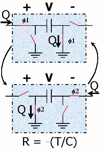
2 Resistor & Charge Relationship I + V - I Resistance is defined in terms of current (I) and voltage (V). I = Q t Current is the rate of change of charge. R = V I = V t Q R = V/I Theory-Basic SC and Anadigm-2

3 Switching Charge to a Capacitor Theory-Basic SC and Anadigm-3
4 Switched Capacitor as a Resistor Equivalent resistance Contains no R Goes UP as C goes down Function only of C and clock period (T) Ratios Independent of clocks Depends on capacitor matching Theory-Basic SC and Anadigm-4
5 Why Switched Capacitor? RC constants with only C s Area savings - much smaller for large R Better resistor values Better tolerance; typically ± 1.0% Better matching - typically ± 0.1% Better Linearity Wider range The extras Phase swapping Frequency dependent RC s Theory-Basic SC and Anadigm-5

6 Phase Swapping Theory-Basic SC and Anadigm-6

7 The Clock as a System Reference Corner frequency can be changed by changing the clock frequency Theory-Basic SC and Anadigm-7

8 Switched Capacitor Circuits are Sampled Data Systems Inputs and outputs may be valid only on certain phases Subject to sampled data system constraints φ1 φ2 φ1 φ2 φ1 φ2 Theory-Basic SC and Anadigm-8

9 Expression of Sampled Data Function V t Q t Q 1 = CV 1 V t Q = CV 0 1 Q t φ1 φ2 φ1 φ2 φ1 φ2 Theory-Basic SC and Anadigm-9 t=-2 t=-1 t=0 (= now )
10 Sampled Data Example C2 Qfb0 = C2 Vout 0 Vin C1 Qin Qfb Qi Ci Qi0 = Ci ( Vout0 Vout 1) Vout Qin = C Vin C 1 Vin C2 Vout0 + Ci ( Vout0 Vout ) = 0 Theory-Basic SC and Anadigm-10
11 And we get : AnadigmDesigner Simulator Equation! Vin C1 C2 Ci Vout nc i All SC functions are about ratios of capacitors. Normalise all caps connected to an integrator stage to the integrator cap (=C 2 here). So: =1 C1 nc 1 = C i C2 nc2 = C i On φ2 : On φ1 : Vout 1 = ( 1 1 (1 + ) Vout + nc Vin nc Vout0 = Vout 1 ) Theory-Basic SC and Anadigm-11
12 Performance: Programming Boundaries Op-amp dynamics Gain-bandwidth product Op-amp slew rate Loading limits Input offset Limit on filter order Capacitance spread Theory-Basic SC and Anadigm-12
13 Opamp Gain Bandwidth Product 80dB 40dB 0dB 120kHz There is a natural trade-off between bandwidth and gain This knowledge is built into the IPmodules Theory-Basic SC and Anadigm-13
14 Op-amp Slew Rate Defines speed at which large transitions in output voltage are made. The op-amp is no longer operating in small-signal mode (the virtual ground is destroyed temporarily) This is separate to GB product It arises from internal features of the op-amp, and is not a feature of capacitive loading Note: excess capacitive load causes op-amp instability (ringing) Anadigm op-amp s are designed to drive 100pF load at unity gain About 6 or 7 full-size input caps Theory-Basic SC and Anadigm-14
15 Input Offset C3 C2 Vin = 0 C1 Vos Vout V out = V os ( C 1 + C3) C 3 Anadigm 3.3volt products have an internal offset nulling circuit this reduces the effective offset from a few mil-volts to less than 250 microvolts. 5 volt products do not have this feature Theory-Basic SC and Anadigm-15
16 Filter Order In theory, very large filters can be constructed with Anadigm s dpasp and FPAA products, 8 poles with each device and multiple devices can be used. All the previous effects are cumulative and will put a practical limit on filters that can be built. A rule of thumb, a maximum order of about can be realised without special consideration of the second order effects mentioned previously (e.g. C-message telecoms filter) Higher order filters with poles in their transfer function (IIR filters) are not often called for anyway. Theory-Basic SC and Anadigm-16
17 Capacitance Spread The ratio of C max to C min in a given Switched Capacitor stage Limits CAM parameter ranges Lowest filter cut-off frequency Minimum and maximum gain settings Maximum length of integrator time-constant Theory-Basic SC and Anadigm-17
18 Extending Capacitance Spread C3 C2a C2b Vin C1 Vout Uses parallel combinations of available capacitors Many of Anadigm s CAM use this technique. Theory-Basic SC and Anadigm-18
Switched-Capacitor Circuits David Johns and Ken Martin University of Toronto
 Switched-Capacitor Circuits David Johns and Ken Martin University of Toronto (johns@eecg.toronto.edu) (martin@eecg.toronto.edu) University of Toronto 1 of 60 Basic Building Blocks Opamps Ideal opamps usually
Sample-and-Holds David Johns and Ken Martin University of Toronto
 Sample-and-Holds David Johns and Ken Martin (johns@eecg.toronto.edu) (martin@eecg.toronto.edu) slide 1 of 18 Sample-and-Hold Circuits Also called track-and-hold circuits Often needed in A/D converters
System on a Chip. Prof. Dr. Michael Kraft
 System on a Chip Prof. Dr. Michael Kraft Lecture 3: Sample and Hold Circuits Switched Capacitor Circuits Circuits and Systems Sampling Signal Processing Sample and Hold Analogue Circuits Switched Capacitor
Switched Capacitor Circuits I. Prof. Paul Hasler Georgia Institute of Technology
 Switched Capacitor Circuits I Prof. Paul Hasler Georgia Institute of Technology Switched Capacitor Circuits Making a resistor using a capacitor and switches; therefore resistance is set by a digital clock
EE247 Analog-Digital Interface Integrated Circuits
 EE247 Analog-Digital Interface Integrated Circuits Fall 200 Name: Zhaoyi Kang SID: 22074 ******************************************************************************* EE247 Analog-Digital Interface Integrated
Homework Assignment 11
 Homework Assignment Question State and then explain in 2 3 sentences, the advantage of switched capacitor filters compared to continuous-time active filters. (3 points) Continuous time filters use resistors
Lecture 7, ATIK. Continuous-time filters 2 Discrete-time filters
 Lecture 7, ATIK Continuous-time filters 2 Discrete-time filters What did we do last time? Switched capacitor circuits with nonideal effects in mind What should we look out for? What is the impact on system
Discrete Time Signals and Switched Capacitor Circuits (rest of chapter , 10.2)
") Discrete Time Signals and Switched Capacitor Circuits (rest of chapter 9 + 0., 0.2) Tuesday 6th of February, 200, 9:5 :45 Snorre Aunet, sa@ifi.uio.no Nanoelectronics Group, Dept. of Informatics Office
Discrete Time Signals and Switched Capacitor Circuits (rest of chapter 9 + 0., 0.2) Tuesday 6th of February, 200, 9:5 :45 Snorre Aunet, sa@ifi.uio.no Nanoelectronics Group, Dept. of Informatics Office
Discrete Time Signals and Switched Capacitor Circuits (rest of chapter , 10.2)
") Discrete Time Signals and Switched Capacitor Circuits (rest of chapter 9 + 10.1, 10.2) Tuesday 16th of February, 2010, 0, 9:15 11:45 Snorre Aunet, sa@ifi.uio.no Nanoelectronics Group, Dept. of Informatics
Discrete Time Signals and Switched Capacitor Circuits (rest of chapter 9 + 10.1, 10.2) Tuesday 16th of February, 2010, 0, 9:15 11:45 Snorre Aunet, sa@ifi.uio.no Nanoelectronics Group, Dept. of Informatics
Advanced Current Mirrors and Opamps
 Advanced Current Mirrors and Opamps David Johns and Ken Martin (johns@eecg.toronto.edu) (martin@eecg.toronto.edu) slide 1 of 26 Wide-Swing Current Mirrors I bias I V I in out out = I in V W L bias ------------
Georgia Institute of Technology School of Electrical and Computer Engineering. Midterm-1 Exam (Solution)
") Georgia Institute of Technology School of Electrical and Computer Engineering Midterm-1 Exam (Solution) ECE-6414 Spring 2012 Friday, Feb. 17, 2012 Duration: 50min First name Solutions Last name Solutions
Georgia Institute of Technology School of Electrical and Computer Engineering Midterm-1 Exam (Solution) ECE-6414 Spring 2012 Friday, Feb. 17, 2012 Duration: 50min First name Solutions Last name Solutions
Lab #4 Capacitors and Inductors. Capacitor Transient and Steady State Response
 Capacitor Transient and Steady State Response Like resistors, capacitors are also basic circuit elements. Capacitors come in a seemingly endless variety of shapes and sizes, and they can all be represented
Lecture 6, ATIK. Switched-capacitor circuits 2 S/H, Some nonideal effects Continuous-time filters
 Lecture 6, ATIK Switched-capacitor circuits 2 S/H, Some nonideal effects Continuous-time filters What did we do last time? Switched capacitor circuits The basics Charge-redistribution analysis Nonidealties
EE100Su08 Lecture #9 (July 16 th 2008)
") EE100Su08 Lecture #9 (July 16 th 2008) Outline HW #1s and Midterm #1 returned today Midterm #1 notes HW #1 and Midterm #1 regrade deadline: Wednesday, July 23 rd 2008, 5:00 pm PST. Procedure: HW #1: Bart
EE100Su08 Lecture #9 (July 16 th 2008) Outline HW #1s and Midterm #1 returned today Midterm #1 notes HW #1 and Midterm #1 regrade deadline: Wednesday, July 23 rd 2008, 5:00 pm PST. Procedure: HW #1: Bart
DESIGN MICROELECTRONICS ELCT 703 (W17) LECTURE 3: OP-AMP CMOS CIRCUIT. Dr. Eman Azab Assistant Professor Office: C
 LECTURE 3: OP-AMP CMOS CIRCUIT. Dr. Eman Azab Assistant Professor Office: C") MICROELECTRONICS ELCT 703 (W17) LECTURE 3: OP-AMP CMOS CIRCUIT DESIGN Dr. Eman Azab Assistant Professor Office: C3.315 E-mail: eman.azab@guc.edu.eg 1 TWO STAGE CMOS OP-AMP It consists of two stages: First
MICROELECTRONICS ELCT 703 (W17) LECTURE 3: OP-AMP CMOS CIRCUIT DESIGN Dr. Eman Azab Assistant Professor Office: C3.315 E-mail: eman.azab@guc.edu.eg 1 TWO STAGE CMOS OP-AMP It consists of two stages: First
Chapter 2 Switched-Capacitor Circuits
 Chapter 2 Switched-Capacitor Circuits Abstract his chapter introduces SC circuits. A brief description is given for the main building blocks of a SC filter (operational amplifiers, switches, capacitors,
Frequency Dependent Aspects of Op-amps
 Frequency Dependent Aspects of Op-amps Frequency dependent feedback circuits The arguments that lead to expressions describing the circuit gain of inverting and non-inverting amplifier circuits with resistive
OPAMPs I: The Ideal Case
 I: The Ideal Case The basic composition of an operational amplifier (OPAMP) includes a high gain differential amplifier, followed by a second high gain amplifier, followed by a unity gain, low impedance,
Sophomore Physics Laboratory (PH005/105)
") CALIFORNIA INSTITUTE OF TECHNOLOGY PHYSICS MATHEMATICS AND ASTRONOMY DIVISION Sophomore Physics Laboratory (PH5/15) Analog Electronics Active Filters Copyright c Virgínio de Oliveira Sannibale, 23 (Revision
CALIFORNIA INSTITUTE OF TECHNOLOGY PHYSICS MATHEMATICS AND ASTRONOMY DIVISION Sophomore Physics Laboratory (PH5/15) Analog Electronics Active Filters Copyright c Virgínio de Oliveira Sannibale, 23 (Revision
ECE 546 Lecture 11 MOS Amplifiers
 ECE 546 Lecture MOS Amplifiers Spring 208 Jose E. Schutt-Aine Electrical & Computer Engineering University of Illinois jesa@illinois.edu ECE 546 Jose Schutt Aine Amplifiers Definitions Used to increase
D is the voltage difference = (V + - V - ).
.") 1 Operational amplifier is one of the most common electronic building blocks used by engineers. It has two input terminals: V + and V -, and one output terminal Y. It provides a gain A, which is usually
1 Operational amplifier is one of the most common electronic building blocks used by engineers. It has two input terminals: V + and V -, and one output terminal Y. It provides a gain A, which is usually
Prof. Anyes Taffard. Physics 120/220. Voltage Divider Capacitor RC circuits
 Prof. Anyes Taffard Physics 120/220 Voltage Divider Capacitor RC circuits Voltage Divider The figure is called a voltage divider. It s one of the most useful and important circuit elements we will encounter.
Pipelined multi step A/D converters
 Department of Electrical Engineering Indian Institute of Technology, Madras Chennai, 600036, India 04 Nov 2006 Motivation for multi step A/D conversion Flash converters: Area and power consumption increase
As light level increases, resistance decreases. As temperature increases, resistance decreases. Voltage across capacitor increases with time LDR
 LDR As light level increases, resistance decreases thermistor As temperature increases, resistance decreases capacitor Voltage across capacitor increases with time Potential divider basics: R 1 1. Both
Homework Assignment 08
 Homework Assignment 08 Question 1 (Short Takes) Two points each unless otherwise indicated. 1. Give one phrase/sentence that describes the primary advantage of an active load. Answer: Large effective resistance
Exploring Autonomous Memory Circuit Operation
 Exploring Autonomous Memory Circuit Operation October 21, 2014 Autonomous Au-to-no-mous: Merriam-Webster Dictionary (on-line) a. Existing independently of the whole. b. Reacting independently of the whole.
Alternating Current Circuits. Home Work Solutions
 Chapter 21 Alternating Current Circuits. Home Work s 21.1 Problem 21.11 What is the time constant of the circuit in Figure (21.19). 10 Ω 10 Ω 5.0 Ω 2.0µF 2.0µF 2.0µF 3.0µF Figure 21.19: Given: The circuit
Yet More On Decoupling, Part 5 When Harry Regulator Met Sally Op-Amp Kendall Castor-Perry
 Page 1 of 8 Yet More On Decoupling, Part 5 When Harry Regulator Met Sally Op-Amp Kendall Castor-Perry This article was published on EDN: http://www.edn.com/design/powermanagement/4415318/why-bypass-caps-make-a-difference---part-5--supply-impedanceand-op-amp-interaction
Designing Information Devices and Systems I Spring 2018 Lecture Notes Note 20
 EECS 16A Designing Information Devices and Systems I Spring 2018 Lecture Notes Note 20 Design Example Continued Continuing our analysis for countdown timer circuit. We know for a capacitor C: I = C dv
Feedback design for the Buck Converter
 Feedback design for the Buck Converter Portland State University Department of Electrical and Computer Engineering Portland, Oregon, USA December 30, 2009 Abstract In this paper we explore two compensation
Today. 1/25/11 Physics 262 Lecture 2 Filters. Active Components and Filters. Homework. Lab 2 this week
 /5/ Physics 6 Lecture Filters Today Basics: Analog versus Digital; Passive versus Active Basic concepts and types of filters Passband, Stopband, Cut-off, Slope, Knee, Decibels, and Bode plots Active Components
Fundamentals of Engineering Exam Review Electromagnetic Physics
 Dr. Gregory J. Mazzaro Spring 2018 Fundamentals of Engineering Exam Review Electromagnetic Physics (currently 5-7% of FE exam) THE CITADEL, THE MILITARY COLLEGE OF SOUTH CAROLINA 171 Moultrie Street, Charleston,
Electronics Capacitors
 Electronics Capacitors Wilfrid Laurier University October 9, 2015 Capacitor an electronic device which consists of two conductive plates separated by an insulator Capacitor an electronic device which consists
13 Amp Programmable DC/DC Regulator PTK series. 3.3VDC, 5VDC, or 12VDC Input
 3.3VDC, 5VDC, or 12VDC Input 5-Bit Programmable from 1.3VDC to 3.5VDC or 1.1 to 1.85VDC at 13A Output Ultra-High Efficiency - No Heatsink Required! Remote Sense/Power Good Signal Short Circuit/Over-Voltage
ECE 202 Fall 2013 Final Exam
 ECE 202 Fall 2013 Final Exam December 12, 2013 Circle your division: Division 0101: Furgason (8:30 am) Division 0201: Bermel (9:30 am) Name (Last, First) Purdue ID # There are 18 multiple choice problems
ECE2262 Electric Circuits. Chapter 6: Capacitance and Inductance
 ECE2262 Electric Circuits Chapter 6: Capacitance and Inductance Capacitors Inductors Capacitor and Inductor Combinations Op-Amp Integrator and Op-Amp Differentiator 1 CAPACITANCE AND INDUCTANCE Introduces
Advanced Analog Integrated Circuits. Operational Transconductance Amplifier II Multi-Stage Designs
 Advanced Analog Integrated Circuits Operational Transconductance Amplifier II Multi-Stage Designs Bernhard E. Boser University of California, Berkeley boser@eecs.berkeley.edu Copyright 2016 by Bernhard
UNIVERSITÀ DEGLI STUDI DI CATANIA. Dottorato di Ricerca in Ingegneria Elettronica, Automatica e del Controllo di Sistemi Complessi, XXII ciclo
 UNIVERSITÀ DEGLI STUDI DI CATANIA DIPARTIMENTO DI INGEGNERIA ELETTRICA, ELETTRONICA E DEI SISTEMI Dottorato di Ricerca in Ingegneria Elettronica, Automatica e del Controllo di Sistemi Complessi, XXII ciclo
Chapter 9 Frequency Response. PART C: High Frequency Response
 Chapter 9 Frequency Response PART C: High Frequency Response Discrete Common Source (CS) Amplifier Goal: find high cut-off frequency, f H 2 f H is dependent on internal capacitances V o Load Resistance
OPERATIONAL AMPLIFIER APPLICATIONS
 OPERATIONAL AMPLIFIER APPLICATIONS 2.1 The Ideal Op Amp (Chapter 2.1) Amplifier Applications 2.2 The Inverting Configuration (Chapter 2.2) 2.3 The Non-inverting Configuration (Chapter 2.3) 2.4 Difference
EE 321 Analog Electronics, Fall 2013 Homework #3 solution
 EE 32 Analog Electronics, Fall 203 Homework #3 solution 2.47. (a) Use superposition to show that the output of the circuit in Fig. P2.47 is given by + [ Rf v N + R f v N2 +... + R ] f v Nn R N R N2 R [
0 t < 0 1 t 1. u(t) =
 =") A. M. Niknejad University of California, Berkeley EE 100 / 42 Lecture 13 p. 22/33 Step Response A unit step function is described by u(t) = ( 0 t < 0 1 t 1 While the waveform has an artificial jump (difficult
A. M. Niknejad University of California, Berkeley EE 100 / 42 Lecture 13 p. 22/33 Step Response A unit step function is described by u(t) = ( 0 t < 0 1 t 1 While the waveform has an artificial jump (difficult
MAU100 Series. 1W, Miniature SIP, Single & Dual Output DC/DC Converters MINMAX. Key Features
 W, Miniature SIP, Single & Dual Output DC/DC s Key Features Efficiency up to % 000 Isolation MTBF >,000,000 Hours Low Cost Input,, and Output 3.3,,9,,,{,{9,{ and { Temperature Performance -0] to +] UL
Danger High Voltage! Your friend starts to climb on this... You shout Get away! That s High Voltage!!! After you save his life, your friend asks:
 Danger High Voltage! Your friend starts to climb on this... You shout Get away! That s High Voltage!!! After you save his life, your friend asks: What is Voltage anyway? Voltage... Is the energy (U, in
Switched Capacitor Circuits II. Dr. Paul Hasler Georgia Institute of Technology
 Switched Capacitor Circuits II Dr. Paul Hasler Georgia Institute of Technology Basic Switch-Cap Integrator = [n-1] - ( / ) H(jω) = - ( / ) 1 1 - e -jωt ~ - ( / ) / jωt (z) - z -1 1 (z) = H(z) = - ( / )
Operational Amplifiers
 NDSU Operational Amplifiers ECE 06 JSG Operational Amplifiers An operational amplifier is a input device with V o k(v V ) where k is a large number. For short, the following symbol is used for an differential
CE/CS Amplifier Response at High Frequencies
 .. CE/CS Amplifier Response at High Frequencies INEL 4202 - Manuel Toledo August 20, 2012 INEL 4202 - Manuel Toledo CE/CS High Frequency Analysis 1/ 24 Outline.1 High Frequency Models.2 Simplified Method.3
Feedback Control G 1+FG A
 Introduction to Operational Amplifiers Circuit Functionality So far, only passive circuits (C, L and LC) have been analyzed in terms of the time-domain operator T and the frequency-domain operator A(ω),
ECEN 607 (ESS) Op-Amps Stability and Frequency Compensation Techniques. Analog & Mixed-Signal Center Texas A&M University
 Op-Amps Stability and Frequency Compensation Techniques. Analog & Mixed-Signal Center Texas A&M University") ECEN 67 (ESS) Op-Amps Stability and Frequency Compensation Techniques Analog & Mixed-Signal Center Texas A&M University Stability of Linear Systems Harold S. Black, 97 Negative feedback concept Negative
ECEN 67 (ESS) Op-Amps Stability and Frequency Compensation Techniques Analog & Mixed-Signal Center Texas A&M University Stability of Linear Systems Harold S. Black, 97 Negative feedback concept Negative
Design of Analog Integrated Circuits
 Design of Analog Integrated Circuits Chapter 11: Introduction to Switched- Capacitor Circuits Textbook Chapter 13 13.1 General Considerations 13.2 Sampling Switches 13.3 Switched-Capacitor Amplifiers 13.4
ECE Spring 2017 Final Exam
 ECE 20100 Spring 2017 Final Exam May 2, 2017 Section (circle below) Qi (12:30) 0001 Tan (10:30) 0004 Hosseini (7:30) 0005 Cui (1:30) 0006 Jung (11:30) 0007 Lin (9:30) 0008 Peleato-Inarrea (2:30) 0009 Name
PHYS225 Lecture 9. Electronic Circuits
 PHYS225 Lecture 9 Electronic Circuits Last lecture Field Effect Transistors Voltage controlled resistor Various FET circuits Switch Source follower Current source Similar to BJT Draws no input current
ECEN 326 Electronic Circuits
 ECEN 326 Electronic Circuits Stability Dr. Aydın İlker Karşılayan Texas A&M University Department of Electrical and Computer Engineering Ideal Configuration V i Σ V ε a(s) V o V fb f a(s) = V o V ε (s)
Coulomb s constant k = 9x10 9 N m 2 /C 2
 1 Part 2: Electric Potential 2.1: Potential (Voltage) & Potential Energy q 2 Potential Energy of Point Charges Symbol U mks units [Joules = J] q 1 r Two point charges share an electric potential energy
Stability & Compensation
 Advanced Analog Building Blocks Stability & Compensation Wei SHEN (KIP) 1 Bode Plot real zeros zeros with complex conjugates real poles poles with complex conjugates http://lpsa.swarthmore.edu/bode/bode.html
PURPOSE: See suggested breadboard configuration on following page!
 ECE4902 Lab 1 C2011 PURPOSE: Determining Capacitance with Risetime Measurement Reverse Biased Diode Junction Capacitance MOSFET Gate Capacitance Simulation: SPICE Parameter Extraction, Transient Analysis
Low-Sensitivity, Highpass Filter Design with Parasitic Compensation
 Low-Sensitivity, Highpass Filter Design with Parasitic Compensation Introduction This Application Note covers the design of a Sallen-Key highpass biquad. This design gives low component and op amp sensitivities.
Electronic Circuits Summary
 Electronic Circuits Summary Andreas Biri, D-ITET 6.06.4 Constants (@300K) ε 0 = 8.854 0 F m m 0 = 9. 0 3 kg k =.38 0 3 J K = 8.67 0 5 ev/k kt q = 0.059 V, q kt = 38.6, kt = 5.9 mev V Small Signal Equivalent
388 Facta Universitatis ser.: Elec. and Energ. vol. 14, No. 3, Dec A 0. The input-referred op. amp. offset voltage V os introduces an output off
 FACTA UNIVERSITATIS (NI»S) Series: Electronics and Energetics vol. 14, No. 3, December 2001, 387-397 A COMPARATIVE STUDY OF TWO SECOND-ORDER SWITCHED-CAPACITOR BALANCED ALL-PASS NETWORKS WITH DIFFERENT
EE105 Fall 2015 Microelectronic Devices and Circuits Frequency Response. Prof. Ming C. Wu 511 Sutardja Dai Hall (SDH)
") EE05 Fall 205 Microelectronic Devices and Circuits Frequency Response Prof. Ming C. Wu wu@eecs.berkeley.edu 5 Sutardja Dai Hall (SDH) Amplifier Frequency Response: Lower and Upper Cutoff Frequency Midband
EE05 Fall 205 Microelectronic Devices and Circuits Frequency Response Prof. Ming C. Wu wu@eecs.berkeley.edu 5 Sutardja Dai Hall (SDH) Amplifier Frequency Response: Lower and Upper Cutoff Frequency Midband
MAU100 Series. 1W, Miniature SIP, Single & Dual Output DC/DC Converters MINMAX. Block Diagram. Key Features
 MAU Series W, Miniature SIP, Single & DC/DC s Key Features Efficiency up to 0 Isolation MTBF >,000,000 Hours Low Cost Input,, and Output 3.3,,9,,,{,{9,{ and { Temperature Performance -0 to UL 9V-0 Package
ENERGY AND TIME CONSTANTS IN RC CIRCUITS By: Iwana Loveu Student No Lab Section: 0003 Date: February 8, 2004
 ENERGY AND TIME CONSTANTS IN RC CIRCUITS By: Iwana Loveu Student No. 416 614 5543 Lab Section: 0003 Date: February 8, 2004 Abstract: Two charged conductors consisting of equal and opposite charges forms
DESIGN OF CMOS ANALOG INTEGRATED CIRCUITS
 DESIGN OF CMOS ANALOG INTEGRATED CIRCUITS Franco Maloberti Integrated Microsistems Laboratory University of Pavia Continuous Time and Switched Capacitor Filters F. Maloberti: Design of CMOS Analog Integrated
RC, RL, and LCR Circuits
 RC, RL, and LCR Circuits EK307 Lab Note: This is a two week lab. Most students complete part A in week one and part B in week two. Introduction: Inductors and capacitors are energy storage devices. They
Pre-Lab. Introduction
 Pre-Lab Read through this entire lab. Perform all of your calculations (calculated values) prior to making the required circuit measurements. You may need to measure circuit component values to obtain
MAU200 Series. 1W, High Isolation SIP, Single & Dual Output DC/DC Converters MINMAX. Block Diagram. Key Features
 Component Distributors, Inc. ~ www.cdiweb.com ~ sales@cdiweb.com ~ -0--33 W, High Isolation SIP, Single & DC/DC s Key Features Efficiency up to 00 Isolation MTBF >,000,000 Hours Low Cost Input, and Output
Time Varying Circuit Analysis
 MAS.836 Sensor Systems for Interactive Environments th Distributed: Tuesday February 16, 2010 Due: Tuesday February 23, 2010 Problem Set # 2 Time Varying Circuit Analysis The purpose of this problem set
ECE2210 Final given: Spring 08
 ECE Final given: Spring 0. Note: feel free to show answers & work right on the schematic 1. (1 pts) The ammeter, A, reads 30 ma. a) The power dissipated by R is 0.7 W, what is the value of R. Assume that
Lecture 4: Feedback and Op-Amps
 Lecture 4: Feedback and Op-Amps Last time, we discussed using transistors in small-signal amplifiers If we want a large signal, we d need to chain several of these small amplifiers together There s a problem,
Electronic Circuits. Prof. Dr. Qiuting Huang Integrated Systems Laboratory
 Electronic Circuits Prof. Dr. Qiuting Huang 6. Transimpedance Amplifiers, Voltage Regulators, Logarithmic Amplifiers, Anti-Logarithmic Amplifiers Transimpedance Amplifiers Sensing an input current ii in
Bipolar Emitter-Follower: Riso w/dual Feedback
 Operational Amplifier Stability Part 10 of 15: Capacitor Loop Stability: Riso with Dual Feedback by Tim Green Linear Applications Engineering Manager, Burr-Brown Products from Texas Instruments Part 10
Start with the transfer function for a second-order high-pass. s 2. ω o. Q P s + ω2 o. = G o V i
 aaac3xicbzfna9taeizxatkk7kec9tilqck4jbg5fjpca4ew0kmpdsrxwhlvxokl7titrirg69lr67s/robll64wmkna5jenndmvjstzyib9pfjntva/vzu6dzsnhj5/sdfefxhmvawzjpotsxeiliemxiucjpogkkybit3x5atow5w8xfugs5qmksecubqo7krlsfhkzsagxr4jne8wehaaxjqy4qq2svvl5el5qai2v9hy5tnxwb0om8igbiqfhhqhkoulcfs2zczhp26lwm7ph/hehffsbu90syo3hcmwvyxpawjtfbjpkm/wlbnximooweuygmsivnygqlpcmywvfppvrewjl3yqxti9gr6e2kgqbgrnlizqyuf2btqd/vgmo8cms4dllesrrdopz4ahyqjf7c66bovhzqznm9l89tqb2smixsxzk3tsdtnat4iaxnkk5bfcbn6iphqywpvxwtypgvnhtsvux234v77/ncudz9leyj84wplgvm7hrmk4ofi7ynw8edpwl7zt62o9klz8kl0idd8pqckq9krmaekz/kt7plbluf3a/un/d7ko6bc0zshbujz6huqq
Application Report. Mixed Signal Products SLOA021
 Application Report May 1999 Mixed Signal Products SLOA021 IMPORTANT NOTICE Texas Instruments and its subsidiaries (TI) reserve the right to make changes to their products or to discontinue any product
Lecture 310 Open-Loop Comparators (3/28/10) Page 310-1
 Page 310-1") Lecture 310 Open-Loop Comparators (3/28/10) Page 310-1 LECTURE 310 OPEN-LOOP COMPARATORS LECTURE ORGANIZATION Outline Characterization of comparators Dominant pole, open-loop comparators Two-pole, open-loop
Lecture 310 Open-Loop Comparators (3/28/10) Page 310-1 LECTURE 310 OPEN-LOOP COMPARATORS LECTURE ORGANIZATION Outline Characterization of comparators Dominant pole, open-loop comparators Two-pole, open-loop
Radivoje Đurić, 2015, Analogna Integrisana Kola 1
 OVA & OTA 1 OVA VA-Operational Voltage Amplifier Ideally a voltage-controlled voltage source Typically contains an output stage that can drive arbitrary loads, including small resistances Predominantly
Operational Amplifiers
 Operational Amplifiers A Linear IC circuit Operational Amplifier (op-amp) An op-amp is a high-gain amplifier that has high input impedance and low output impedance. An ideal op-amp has infinite gain and
Nyquist-Rate D/A Converters. D/A Converter Basics.
 Nyquist-Rate D/A Converters David Johns and Ken Martin (johns@eecg.toronto.edu) (martin@eecg.toronto.edu) slide 1 of 20 D/A Converter Basics. B in D/A is a digital signal (or word), B in b i B in = 2 1
Designing Information Devices and Systems II Fall 2018 Elad Alon and Miki Lustig Discussion 5A
 EECS 6B Designing Information Devices and Systems II Fall 208 Elad Alon and Miki Lustig Discussion 5A Transfer Function When we write the transfer function of an arbitrary circuit, it always takes the
Distributing Tomorrow s Technologies For Today s Designs Toll-Free:
 2W, Ultra-High Isolation DIP, Single & DC/DC s Key Features Low Cost 6 Isolation MTBF > 6, Hours Short Circuit Protection Input, and 24 Output,, 1, {, { and {1 Regulated Outputs Low Isolation Capacitance
EE247 Lecture 19. EECS 247 Lecture 19: Data Converters 2006 H.K. Page 1. Summary Last Lecture
 EE247 Lecture 19 ADC Converters Sampling (continued) Clock boosters (continued) Sampling switch charge injection & clock feedthrough Complementary switch Use of dummy device Bottom-plate switching Track
Lecture 120 Compensation of Op Amps-I (1/30/02) Page ECE Analog Integrated Circuit Design - II P.E. Allen
 Page ECE Analog Integrated Circuit Design - II P.E. Allen") Lecture 20 Compensation of Op AmpsI (/30/02) Page 20 LECTURE 20 COMPENSATION OF OP AMPS I (READING: GHLM 425434 and 624638, AH 249260) INTRODUCTION The objective of this presentation is to present the
Lecture 20 Compensation of Op AmpsI (/30/02) Page 20 LECTURE 20 COMPENSATION OF OP AMPS I (READING: GHLM 425434 and 624638, AH 249260) INTRODUCTION The objective of this presentation is to present the
Laboratory III: Operational Amplifiers
 Physics 33, Fall 2008 Lab III - Handout Laboratory III: Operational Amplifiers Introduction Operational amplifiers are one of the most useful building blocks of analog electronics. Ideally, an op amp would
Spiral 2 7. Capacitance, Delay and Sizing. Mark Redekopp
 2-7.1 Spiral 2 7 Capacitance, Delay and Sizing Mark Redekopp 2-7.2 Learning Outcomes I understand the sources of capacitance in CMOS circuits I understand how delay scales with resistance, capacitance
ECE Networks & Systems
 ECE 342 1. Networks & Systems Jose E. Schutt Aine Electrical & Computer Engineering University of Illinois jschutt@emlab.uiuc.edu 1 What is Capacitance? 1 2 3 Voltage=0 No Charge No Current Voltage build
ELECTRONIC SYSTEMS. Basic operational amplifier circuits. Electronic Systems - C3 13/05/ DDC Storey 1
 Electronic Systems C3 3/05/2009 Politecnico di Torino ICT school Lesson C3 ELECTONIC SYSTEMS C OPEATIONAL AMPLIFIES C.3 Op Amp circuits» Application examples» Analysis of amplifier circuits» Single and
KH600. 1GHz, Differential Input/Output Amplifier. Features. Description. Applications. Typical Application
 KH 1GHz, Differential Input/Output Amplifier www.cadeka.com Features DC - 1GHz bandwidth Fixed 1dB (V/V) gain 1Ω (differential) inputs and outputs -7/-dBc nd/3rd HD at MHz ma output current 9V pp into
KIA7805API~ KIA7824API BIPOLAR LINEAR INTEGRATED CIRCUIT SEMICONDUCTOR TECHNICAL DATA
 SEMICONDUCTOR TECHNICAL DATA KIA785API~ KIA7824API BIPOLAR LINEAR INTEGRATED THREE TERMINAL POSITIVE VOLTAGE REGULATORS 5V, 6V, 8V, 9V, 1V, 12V, 15V, 18V, 2V, 24V. A C FEATURES Suitable for C-MOS, TTL,
Operational amplifiers (Op amps)
") Operational amplifiers (Op amps) v R o R i v i Av i v View it as an ideal amp. Take the properties to the extreme: R i, R o 0, A.?!?!?!?! v v i Av i v A Consequences: No voltage dividers at input or output.
Operational amplifiers (Op amps) v R o R i v i Av i v View it as an ideal amp. Take the properties to the extreme: R i, R o 0, A.?!?!?!?! v v i Av i v A Consequences: No voltage dividers at input or output.
Print Name : ID : ECE Test #1 9/22/2016
 Print Name : Email ID : ECE 2660 Test #1 9/22/2016 All answers must be recorded on the answer page (page 2). You must do all questions on the exam. For Part 4 you must show all your work and write your
Low-Noise Sigma-Delta Capacitance-to-Digital Converter for Sub-pF Capacitive Sensors with Integrated Dielectric Loss Measurement
 Low-Noise Sigma-Delta Capacitance-to-Digital Converter for Sub-pF Capacitive Sensors with Integrated Dielectric Loss Measurement Markus Bingesser austriamicrosystems AG Rietstrasse 4, 864 Rapperswil, Switzerland
Solved Problems. Electric Circuits & Components. 1-1 Write the KVL equation for the circuit shown.
 Solved Problems Electric Circuits & Components 1-1 Write the KVL equation for the circuit shown. 1-2 Write the KCL equation for the principal node shown. 1-2A In the DC circuit given in Fig. 1, find (i)
Designing Information Devices and Systems I Discussion 8B
 EECS 16A Spring 2018 Designing Information Devices and Systems I Discussion 8B 1. Bio-Molecule Detector We ve already seen how to build a bio-molecule detector where bio-molecules change the resistance
Conventional Paper-I Part A. 1. (a) Define intrinsic wave impedance for a medium and derive the equation for intrinsic vy
 Define intrinsic wave impedance for a medium and derive the equation for intrinsic vy") EE-Conventional Paper-I IES-01 www.gateforum.com Conventional Paper-I-01 Part A 1. (a) Define intrinsic wave impedance for a medium and derive the equation for intrinsic vy impedance for a lossy dielectric
EE-Conventional Paper-I IES-01 www.gateforum.com Conventional Paper-I-01 Part A 1. (a) Define intrinsic wave impedance for a medium and derive the equation for intrinsic vy impedance for a lossy dielectric
Exercise 1: Capacitors
 Capacitance AC 1 Fundamentals Exercise 1: Capacitors EXERCISE OBJECTIVE When you have completed this exercise, you will be able to describe the effect a capacitor has on dc and ac circuits by using measured
Massachusetts Institute of Technology Department of Electrical Engineering and Computer Science Electronic Circuits Fall 2000.
 Massachusetts Institute of Technology Department of Electrical Engineering and Computer Science 6.002 Electronic Circuits Fall 2000 Final Exam Please write your name in the space provided below, and circle
Studio 9 Review Operational Amplifier Stability Compensation Miller Effect Phase Margin Unity Gain Frequency Slew Rate Limiting Reading: Text sec 5.
 Studio 9 Review Operational Amplifier Stability Compensation Miller Effect Phase Margin Unity Gain Frequency Slew Rate Limiting Reading: Text sec 5.2 pp. 232-242 Two-stage op-amp Analysis Strategy Recognize
Topic 4. The CMOS Inverter
 Topic 4 The CMOS Inverter Peter Cheung Department of Electrical & Electronic Engineering Imperial College London URL: www.ee.ic.ac.uk/pcheung/ E-mail: p.cheung@ic.ac.uk Topic 4-1 Noise in Digital Integrated
Exercise 1: RC Time Constants
 Exercise 1: RC EXERCISE OBJECTIVE When you have completed this exercise, you will be able to determine the time constant of an RC circuit by using calculated and measured values. You will verify your results
Bandwidth of op amps. R 1 R 2 1 k! 250 k!
 Bandwidth of op amps An experiment - connect a simple non-inverting op amp and measure the frequency response. From the ideal op amp model, we expect the amp to work at any frequency. Is that what happens?
Stability and Frequency Compensation
 類比電路設計 (3349) - 2004 Stability and Frequency ompensation hing-yuan Yang National hung-hsing University Department of Electrical Engineering Overview Reading B Razavi hapter 0 Introduction In this lecture,