Optical Proximity Correction
|
|
|
- Ginger Doyle
- 6 years ago
- Views:
Transcription

1 Optical Proximity Correction Mask Wafer *Auxiliary features added on mask 1
2 Overlay Errors + + alignment mask wafer + + photomask plate Alignment marks from previous masking level 2
3 (1) Thermal run-in/run-out errors R r Tm m Tsi si run-out wafer error radius Tm, Tsi change of mask and wafer temp. m, si coefficient of thermal expansion of mask & Si 3
4 run-out (2) Translational Error Al n+ p image referrer 4
5 (3) Rotational Error 5
6 6
7 Characterization of Overlay Errors T O + y x R L O + + O C + O O + R O =optical image + =alignment marks on wafer wafer B 7
8 Example m x y T R C L B * Center of wafer has only translation error Terror = (0.5, 0.5) After subtracting Terror, 8
9 T x y T R C 0 0 B y x 0.5 R L L B wafer 9
10 Run out error 0.2 m Rotational error 0.5 m [counter clockwise] If wafer diameter is 4" D 10 cm Rotational error 5 10 radians y R 10
11 Optical image of mask alignment marks Reference marks on wafer With thermal run-out, the alignment error is 1/2 of the image/reference difference [best scenario] 11
12 Total Overlay Tolerance 2 i total 2 i th masking step = std. deviation of overlay error for i i total = std. deviation for total overlay error Layout design-rule specification should be > total 12
13 Example: Contact to source/drain of MOSFET. SiO2 SiO2 Al ideal n+ p-si SiO2 Alignment error between oxide opening and n+ pattern SiO2 n+ Al short, ohmic contact p-si 13

14 Solution: Design n+ region larger than contact hole Al SiO2 SiO2 n+ 14
15 Two Resist Types Negative Resist Polymer (Molecular Weight (MW) ~65000) Light Sensitive Additive Promotes Crosslinking Volatile Solvents Light breaks N-N => Crosslink Chains Sensitive, hard, Swelling during Develop Positive Resist Polymer (MW~5000) Photoactive Inhibitor (20%) Volatile Solvents Inhibitor Looses N2 => Alkali Soluble Acid Develops by etching - No Swelling. 15
16 Positive Resist hv mask exposed part is removed 100% (linear scale) E1 P.R. ET = resist sensitivity Resist contrast LOG TO BASE 10 log resist thickness remaining ET exposure photon energy (log scale) ~ 5 to 10 Note: In the 143 Reader, is defined as natural log 16
17 Positive P.R. Mechanism Photons deactivate sensitizer less cross-linking dissolve in developer solution polymer + photosensitizer 17
18 diazide Positive Resist Exposure Reaction ketene - a = C = 0 group The ketene is shortlived intermediate PAC carboxylic acid moisture The carboxylic acid can react with the alkaline solution (the soluble ester developer) to form a soluble ester. 18
19 Chemical Amplified Resist (CAR) For reference only Photo-Acid generator 19 N Cheung EE243 s2010 L
20 Negative P.R. Mechanism hv % remaining mask after development ET 1 E1 log ET E1 photon energy hv => cross-linking => insoluble in developer solution. Log to base 10 20
21 Why High-Contrast Resist is desirable? Optical image Infinite contrast resist resist substrate Finite contrast resist resist substrate Position x 21
22 22
23 Positive vs. Negative Photoresists Positive P.R.: higher resolution aqueous-based solvents less sensitive Negative P.R.: more sensitive => higher exposure throughput relatively tolerant of developing conditions better chemical resistance => better mask material less expensive lower resolution organic-based solvents 23

24 Standing Waves *Photoresist has a finite thickness hv Higher Intensity Faster Development rate Lower Intensity Slower Development rate Positive Photoresist substrate Positive Photoresist. After development substrate 24
25 Standing reflecting wave effect surface Air Photoresist E E E Resist profile and energy deposition depend on oxide thickness underneath (see handout for derivation) 4 3 E 1 Oxide 2 x=0 x=d r x=d T 1 I23 (x) = (E (x)+e3(x))2dt T 2 I23 (max) 0 1 = (E2 - E3)2 + 2E2E3sin2[k(d-x)] I23 (max) = (E2 + E3)2 ; I 23(min) = (E2 - E3)2 2 2 I23 (min) x 2 n In ten sity m in im a occu r at : (d -x) = 0,, 2,... 2 n In ten sity m a x im a occu r a t : (d -x ) = /2, 3, 5,... d 25

26 x P.R. d SiO2/Si substrate Intensity = minimum when x d m Intensity = maximum when x d m n = refractive index of resist 2n 4n m = 0, 1, 2,... m = 1, 3, 5,... 26
27 Simulated Resist Cross-section as function of development time 27

28 Proximity Scattering 28
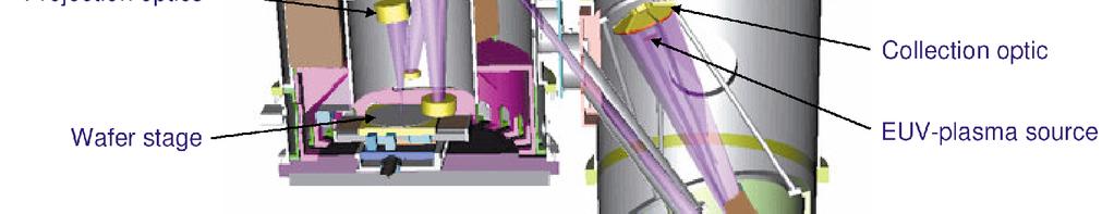
 2: thin develop-stop layer, used for pattern transfer to 3 (etch stop) 3: thick layer of hardened resist (planarization layer)")
29 Approaches for Reducing Substrate Effects Use absorption dyes in photoresist Use anti-reflection coating (ARC) Use multi-layer resist process 1: thin planar layer for high-resolution imaging (imaging layer) 2: thin develop-stop layer, used for pattern transfer to 3 (etch stop) 3: thick layer of hardened resist (planarization layer) 29
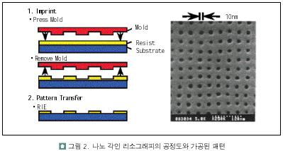
30 Electron-Beam Lithography 12.3 V Angstroms for V in Volts Example: 30 kv e-beam => = 0.07 Angstroms NA = Resolution < 1 nm But beam current needs to be 10 s of ma for a throughput of more than 10 wafers an hour. 30


31 Low Throughput for both raster and vector scanning (Serial Process) Variable Beam-shape EBL Stencil Mask EBL 31
32 The Proximity Effect Monte Carlo simulation of electron trajectories 32
 performance records organic resist PMMA ~ inorganic resist, b.v.")
33 e-beam lithography resolution factors beam quality ( ~1 nm) secondary electrons ( lateral range: few nm) performance records organic resist PMMA ~ inorganic resist, b.v. AlF3 ~ 7 nm 1-2 nm 33

34 Immersion Lithography A liquid with index of refraction n>1 is introduced between the imaging optics and the wafer. liquid = air /n With water, the index of refraction at = 193 nm is 1.44, improving the resolution significantly. 34
35 Phase-Shifting Mask For resolution enhancement. Example shown is an alternating PSM


36 EUV Lithography =11.2 nm 36


37 Schematic for EUV Litho Mo-Si Reflective Mask reflectivity 37 N Cheung EE243S05 Lec
38 Nanoimprinting 38 N Cheung EE243S05 Lec
 ~ 23 Areal")
39 Why photolithography? High throughput Empirical : Resolution (in Å) ~ 23 Areal Throughput (in um2/hr) N Cheung EE243S05 Lec
40 40


41 Hands On Exploration of Images A web browser-based simulator of lithography 41
Introduction. Photoresist : Type: Structure:
 Photoresist SEM images of the morphologies of meso structures and nanopatterns on (a) a positively nanopatterned silicon mold, and (b) a negatively nanopatterned silicon mold. Introduction Photoresist
UNIVERSITY OF CALIFORNIA College of Engineering Department of Electrical Engineering and Computer Sciences. Professor Ali Javey. Spring 2009.
 UNIVERSITY OF CALIFORNIA College of Engineering Department of Electrical Engineering and Computer Sciences EE143 Professor Ali Javey Spring 2009 Exam 1 Name: SID: Closed book. One sheet of notes is allowed.
Lecture 8. Photoresists and Non-optical Lithography
 Lecture 8 Photoresists and Non-optical Lithography Reading: Chapters 8 and 9 and notes derived from a HIGHLY recommended book by Chris Mack, Fundamental Principles of Optical Lithography. Any serious student
Techniken der Oberflächenphysik (Techniques of Surface Physics)
") Techniken der Oberflächenphysik (Techniques of Surface Physics) Prof. Yong Lei & Dr. Yang Xu (& Liying Liang) Fachgebiet 3D-Nanostrukturierung, Institut für Physik Contact: yong.lei@tu-ilmenau.de; yang.xu@tu-ilmenau.de;
Techniken der Oberflächenphysik (Techniques of Surface Physics) Prof. Yong Lei & Dr. Yang Xu (& Liying Liang) Fachgebiet 3D-Nanostrukturierung, Institut für Physik Contact: yong.lei@tu-ilmenau.de; yang.xu@tu-ilmenau.de;
Photolithography 光刻 Part II: Photoresists
 微纳光电子材料与器件工艺原理 Photolithography 光刻 Part II: Photoresists Xing Sheng 盛兴 Department of Electronic Engineering Tsinghua University xingsheng@tsinghua.edu.cn 1 Photolithography 光刻胶 负胶 正胶 4 Photolithography
UNIT 3. By: Ajay Kumar Gautam Asst. Prof. Dev Bhoomi Institute of Technology & Engineering, Dehradun
 UNIT 3 By: Ajay Kumar Gautam Asst. Prof. Dev Bhoomi Institute of Technology & Engineering, Dehradun 1 Syllabus Lithography: photolithography and pattern transfer, Optical and non optical lithography, electron,
5. Photochemistry of polymers
 5. Photochemistry of polymers 5.1 Photopolymerization and cross-linking Photopolymerization The fundamental principle of photopolymerization is based on the photoinduced production of a reactive species,
Introduction to Photolithography
 http://www.ichaus.de/news/72 Introduction to Photolithography Photolithography The following slides present an outline of the process by which integrated circuits are made, of which photolithography is
MSN551 LITHOGRAPHY II
 MSN551 Introduction to Micro and Nano Fabrication LITHOGRAPHY II E-Beam, Focused Ion Beam and Soft Lithography Why need electron beam lithography? Smaller features are required By electronics industry:
Pattern Transfer- photolithography
 Pattern Transfer- photolithography DUV : EUV : 13 nm 248 (KrF), 193 (ArF), 157 (F 2 )nm H line: 400 nm I line: 365 nm G line: 436 nm Wavelength (nm) High pressure Hg arc lamp emission Ref: Campbell: 7
Lecture 14 Advanced Photolithography
 Lecture 14 Advanced Photolithography Chapter 14 Wolf and Tauber 1/74 Announcements Term Paper: You are expected to produce a 4-5 page term paper on a selected topic (from a list). Term paper contributes
MICRO AND NANOPROCESSING TECHNOLOGIES
 LECTURE 5 MICRO AND NANOPROCESSING TECHNOLOGIES Introduction Ion lithography X-ray lithography Soft lithography E-beam lithography Concepts and processes Lithography systems Masks and resists Chapt.9.
MEEN Nanoscale Issues in Manufacturing. Lithography Lecture 1: The Lithographic Process
 MEEN 489-500 Nanoscale Issues in Manufacturing Lithography Lecture 1: The Lithographic Process 1 Discuss Reading Assignment 1 1 Introducing Nano 2 2 Size Matters 3 3 Interlude One-The Fundamental Science
IC Fabrication Technology
 IC Fabrication Technology * History: 1958-59: J. Kilby, Texas Instruments and R. Noyce, Fairchild * Key Idea: batch fabrication of electronic circuits n entire circuit, say 10 7 transistors and 5 levels
Table of Contents. Foreword... Jörge DE SOUSA NORONHA. Introduction... Michel BRILLOUËT
 Table of Contents Foreword... Jörge DE SOUSA NORONHA Introduction... Michel BRILLOUËT xi xvii Chapter 1. Photolithography... 1 Philippe BANDELIER, Anne-Laure CHARLEY and Alexandre LAGRANGE 1.1. Introduction...
Top down and bottom up fabrication
 Lecture 24 Top down and bottom up fabrication Lithography ( lithos stone / graphein to write) City of words lithograph h (Vito Acconci, 1999) 1930 s lithography press Photolithography d 2( NA) NA=numerical
Lithography and Etching
 Lithography and Etching Victor Ovchinnikov Chapters 8.1, 8.4, 9, 11 Previous lecture Microdevices Main processes: Thin film deposition Patterning (lithography) Doping Materials: Single crystal (monocrystal)
The Monte Carlo Simulation of Secondary Electrons Excitation in the Resist PMMA
 Applied Physics Research; Vol. 6, No. 3; 204 ISSN 96-9639 E-ISSN 96-9647 Published by Canadian Center of Science and Education The Monte Carlo Simulation of Secondary Electrons Excitation in the Resist
Photomasks. Photolithography Evolution 9/11/2004 ECE580- MPE/MASKS/PHOTOMASKS.PPT
 Photolithography Evolution 1 : Evolution 2 Photomasks Substrates: Type : thermal expansion Chrome Pellicles Mask: OPC and PSM Fabrication: E-Beam or Laser 3 Photomask Information Websites: http://www.photronics.com/internet/corpcomm/publications/basics101/basics.
Reactive Ion Etching (RIE)
") Reactive Ion Etching (RIE) RF 13.56 ~ MHz plasma Parallel-Plate Reactor wafers Sputtering Plasma generates (1) Ions (2) Activated neutrals Enhance chemical reaction 1 2 Remote Plasma Reactors Plasma Sources
Reactive Ion Etching (RIE) RF 13.56 ~ MHz plasma Parallel-Plate Reactor wafers Sputtering Plasma generates (1) Ions (2) Activated neutrals Enhance chemical reaction 1 2 Remote Plasma Reactors Plasma Sources
There's Plenty of Room at the Bottom
 There's Plenty of Room at the Bottom 12/29/1959 Feynman asked why not put the entire Encyclopedia Britannica (24 volumes) on a pin head (requires atomic scale recording). He proposed to use electron microscope
Photolithography Overview 9/29/03 Brainerd/photoclass/ECE580/Overvie w/overview
 http://www.intel.com/research/silicon/mooreslaw.htm 1 Moore s law only holds due to photolithography advancements in reducing linewidths 2 All processing to create electric components and circuits rely
Nanostructures Fabrication Methods
 Nanostructures Fabrication Methods bottom-up methods ( atom by atom ) In the bottom-up approach, atoms, molecules and even nanoparticles themselves can be used as the building blocks for the creation of
Chapter 3 : ULSI Manufacturing Technology - (c) Photolithography
 Photolithography") Chapter 3 : ULSI Manufacturing Technology - (c) Photolithography 1 Reference 1. Semiconductor Manufacturing Technology : Michael Quirk and Julian Serda (2001) 2. - (2004) 3. Semiconductor Physics and Devices-
Chapter 3 : ULSI Manufacturing Technology - (c) Photolithography 1 Reference 1. Semiconductor Manufacturing Technology : Michael Quirk and Julian Serda (2001) 2. - (2004) 3. Semiconductor Physics and Devices-
Development of Lift-off Photoresists with Unique Bottom Profile
 Transactions of The Japan Institute of Electronics Packaging Vol. 8, No. 1, 2015 [Technical Paper] Development of Lift-off Photoresists with Unique Bottom Profile Hirokazu Ito, Kouichi Hasegawa, Tomohiro
UNIVERSITY OF CALIFORNIA College of Engineering Department of Electrical Engineering and Computer Sciences. Fall Exam 1
 UNIVERSITY OF CALIFORNIA College of Engineering Department of Electrical Engineering and Computer Sciences EECS 143 Fall 2008 Exam 1 Professor Ali Javey Answer Key Name: SID: 1337 Closed book. One sheet
Nano fabrication by e-beam lithographie
 Introduction to nanooptics, Summer Term 2012, Abbe School of Photonics, FSU Jena, Prof. Thomas Pertsch Nano fabrication by e-beam lithographie Lecture 14 1 Electron Beam Lithography - EBL Introduction
UNIVERSITY OF CALIFORNIA College of Engineering Department of Electrical Engineering and Computer Sciences. Professor Ali Javey. Fall 2009.
 UNIVERSITY OF CALIFORNIA College of Engineering Department of Electrical Engineering and Computer Sciences EE143 Professor Ali Javey Fall 2009 Exam 1 Name: SID: Closed book. One sheet of notes is allowed.
Nanoimprint Lithography
 Nanoimprint Lithography Wei Wu Quantum Science Research Advanced Studies HP Labs, Hewlett-Packard Email: wei.wu@hp.com Outline Background Nanoimprint lithography Thermal based UV-based Applications based
Supplementary Information Our InGaN/GaN multiple quantum wells (MQWs) based one-dimensional (1D) grating structures
 based one-dimensional (1D) grating structures") Polarized white light from hybrid organic/iii-nitrides grating structures M. Athanasiou, R. M. Smith, S. Ghataora and T. Wang* Department of Electronic and Electrical Engineering, University of Sheffield,
Polarized white light from hybrid organic/iii-nitrides grating structures M. Athanasiou, R. M. Smith, S. Ghataora and T. Wang* Department of Electronic and Electrical Engineering, University of Sheffield,
EE115C Winter 2017 Digital Electronic Circuits. Lecture 3: MOS RC Model, CMOS Manufacturing
 EE115C Winter 2017 Digital Electronic Circuits Lecture 3: MOS RC Model, CMOS Manufacturing Agenda MOS Transistor: RC Model (pp. 104-113) S R on D CMOS Manufacturing Process (pp. 36-46) S S C GS G G C GD
EE141- Spring 2003 Lecture 3. Last Lecture
 - Spring 003 Lecture 3 IC Manufacturing 1 Last Lecture Design Metrics (part 1) Today Design metrics (wrap-up) IC manufacturing 1 Administrivia Discussion sessions start this week. Only one this week (Dejan
520/ Photolithography (II) Andreas G. Andreou
 Andreas G. Andreou") 520/580.495 Photolithography (II) Andreas G. Andreou Lecture notes from Positive Photoresists and Photolithography by R. Darling http://www.engr.washington.edu/~cam/processes A.G. Andreou 2000 1 Lecture
520/580.495 Photolithography (II) Andreas G. Andreou Lecture notes from Positive Photoresists and Photolithography by R. Darling http://www.engr.washington.edu/~cam/processes A.G. Andreou 2000 1 Lecture
Lecture 150 Basic IC Processes (10/10/01) Page ECE Analog Integrated Circuits and Systems P.E. Allen
 Page ECE Analog Integrated Circuits and Systems P.E. Allen") Lecture 150 Basic IC Processes (10/10/01) Page 1501 LECTURE 150 BASIC IC PROCESSES (READING: TextSec. 2.2) INTRODUCTION Objective The objective of this presentation is: 1.) Introduce the fabrication of
Lecture 150 Basic IC Processes (10/10/01) Page 1501 LECTURE 150 BASIC IC PROCESSES (READING: TextSec. 2.2) INTRODUCTION Objective The objective of this presentation is: 1.) Introduce the fabrication of
Photolithography II ( Part 1 )
") 1 Photolithography II ( Part 1 ) Chapter 14 : Semiconductor Manufacturing Technology by M. Quirk & J. Serda Bjørn-Ove Fimland, Department of Electronics and Telecommunication, Norwegian University of Science
1 Photolithography II ( Part 1 ) Chapter 14 : Semiconductor Manufacturing Technology by M. Quirk & J. Serda Bjørn-Ove Fimland, Department of Electronics and Telecommunication, Norwegian University of Science
Make sure the exam paper has 9 pages (including cover page) + 3 pages of data for reference
 + 3 pages of data for reference") UNIVERSITY OF CALIFORNIA College of Engineering Department of Electrical Engineering and Computer Sciences Spring 2006 EE143 Midterm Exam #1 Family Name First name SID Signature Make sure the exam paper
UNIVERSITY OF CALIFORNIA College of Engineering Department of Electrical Engineering and Computer Sciences Spring 2006 EE143 Midterm Exam #1 Family Name First name SID Signature Make sure the exam paper
EE143 LAB. Professor N Cheung, U.C. Berkeley
 EE143 LAB 1 1 EE143 Equipment in Cory 218 2 Guidelines for Process Integration * A sequence of Additive and Subtractive steps with lateral patterning Processing Steps Si wafer Watch out for materials compatibility
Introduction to Electron Beam Lithography
 Introduction to Electron Beam Lithography Boštjan Berčič (bostjan.bercic@ijs.si), Jožef Štefan Institute, Jamova 39, 1000 Ljubljana, Slovenia 1. Introduction Electron Beam Lithography is a specialized
Carrier Transport by Diffusion
 Carrier Transport by Diffusion Holes diffuse ÒdownÓ the concentration gradient and carry a positive charge --> hole diffusion current has the opposite sign to the gradient in hole concentration dp/dx p(x)
DQN Positive Photoresist
 UNIVESITY OF CALIFONIA, BEKELEY BEKELEY DAVIS IVINE LOS ANGELES IVESIDE SAN DIEGO SAN FANCISCO SANTA BABAA SANTA CUZ DEPATMENT OF BIOENGINEEING 94720-1762 BioE 121 Midterm #1 Solutions BEKELEY, CALIFONIA
CURRENT STATUS OF NANOIMPRINT LITHOGRAPHY DEVELOPMENT IN CNMM
 U.S. -KOREA Forums on Nanotechnology 1 CURRENT STATUS OF NANOIMPRINT LITHOGRAPHY DEVELOPMENT IN CNMM February 17 th 2005 Eung-Sug Lee,Jun-Ho Jeong Korea Institute of Machinery & Materials U.S. -KOREA Forums
Techniques for directly measuring the absorbance of photoresists at EUV wavelengths
 Techniques for directly measuring the absorbance of photoresists at EUV wavelengths Manish Chandhok, a Heidi Cao, a Wang Yueh, a Eric Gullikson, b Robert Brainard, c Stewart Robertson c a Intel Corporation,
Overview of the main nano-lithography techniques
 Overview of the main nano-lithography techniques Soraya Sangiao sangiao@unizar.es Outline Introduction: Nanotechnology. Nano-lithography techniques: Masked lithography techniques: Photolithography. X-ray
Section 3: Etching. Jaeger Chapter 2 Reader
 Section 3: Etching Jaeger Chapter 2 Reader Etch rate Etch Process - Figures of Merit Etch rate uniformity Selectivity Anisotropy d m Bias and anisotropy etching mask h f substrate d f d m substrate d f
FLCC Seminar. Spacer Lithography for Reduced Variability in MOSFET Performance
 1 Seminar Spacer Lithography for Reduced Variability in MOSFET Performance Prof. Tsu-Jae King Liu Electrical Engineering & Computer Sciences Dept. University of California at Berkeley Graduate Student:
4FNJDPOEVDUPS 'BCSJDBUJPO &UDI
 2010.5.4 1 Major Fabrication Steps in CMOS Process Flow UV light oxygen Silicon dioxide Silicon substrate Oxidation (Field oxide) photoresist Photoresist Coating Mask exposed photoresist Mask-Wafer Exposed
EE130: Integrated Circuit Devices
 EE130: Integrated Circuit Devices (online at http://webcast.berkeley.edu) Instructor: Prof. Tsu-Jae King (tking@eecs.berkeley.edu) TA s: Marie Eyoum (meyoum@eecs.berkeley.edu) Alvaro Padilla (apadilla@eecs.berkeley.edu)
EE C245 ME C218 Introduction to MEMS Design Fall 2007
 EE C245 ME C218 Introduction to MEMS Design Fall 2007 Prof. Clark T.-C. Nguyen Dept. of Electrical Engineering & Computer Sciences University of California at Berkeley Berkeley, CA 94720 Lecture 5: ALD,
High NA the Extension Path of EUV Lithography. Dr. Tilmann Heil, Carl Zeiss SMT GmbH
 High NA the Extension Path of EUV Lithography Dr. Tilmann Heil, Carl Zeiss SMT GmbH Introduction This talk is about resolution. Resolution λ = k 1 NA High-NA NA 0.33 0.4 0.5 0.6 Resolution @ k1=0.3 single
Fabrication Engineering at the Micro- and Nanoscale, by Stephen Campbell, 4 th Edition, Oxford University Press
 Fabrication Engineering at the Micro- and Nanoscale, by Stephen Campbell, 4 th Edition, Oxford University Press Errata, by Chris Mack, chris@lithoguru.com While teaching out of this book at the University
Far IR Gas Lasers microns wavelengths, THz frequency Called Terahertz lasers or FIR lasers At this wavelength behaves more like
 Far IR Gas Lasers 10-1500 microns wavelengths, 300 10 THz frequency Called Terahertz lasers or FIR lasers At this wavelength behaves more like microwave signal than light Created by Molecular vibronic
Make sure the exam paper has 7 pages (including cover page) + 3 pages of data for reference
 + 3 pages of data for reference") UNIVERSITY OF CALIFORNIA College of Engineering Department of Electrical Engineering and Computer Sciences Fall 2005 EE143 Midterm Exam #1 Family Name First name SID Signature Make sure the exam paper
UNIVERSITY OF CALIFORNIA College of Engineering Department of Electrical Engineering and Computer Sciences Fall 2005 EE143 Midterm Exam #1 Family Name First name SID Signature Make sure the exam paper
EE 434 Lecture 7. Process Technology
 EE 434 Lecture 7 Process Technology Quiz 4 How many wafers can be obtained from a 2m pull? Neglect the material wasted in the kerf used to separate the wafers. 2m And the number is. 1 8 3 5 6 4 9 7 2 1
Fabrication-II. Electron Beam Lithography Pattern Design Thin Film Deposition
 Fabrication-II Electron Beam Lithography Pattern Design Thin Film Deposition By Charulata Barge, Graduate student, Prof. Zumbühl Group, Department of Physics, Universtity of Basel. Date:- 20th Oct. 2006
Wet Chemical Processing with Megasonics Assist for the Removal of Bumping Process Photomasks
 Wet Chemical Processing with Megasonics Assist for the Removal of Bumping Process Photomasks Hongseong Sohn and John Tracy Akrion Systems 6330 Hedgewood Drive, Suite 150 Allentown, PA 18106, USA Abstract
After Development Inspection (ADI) Studies of Photo Resist Defectivity of an Advanced Memory Device
 Studies of Photo Resist Defectivity of an Advanced Memory Device") After Development Inspection (ADI) Studies of Photo Resist Defectivity of an Advanced Memory Device Hyung-Seop Kim, Yong Min Cho, Byoung-Ho Lee Semiconductor R&D Center, Device Solution Business, Samsung
After Development Inspection (ADI) Studies of Photo Resist Defectivity of an Advanced Memory Device Hyung-Seop Kim, Yong Min Cho, Byoung-Ho Lee Semiconductor R&D Center, Device Solution Business, Samsung
Ion Implantation. alternative to diffusion for the introduction of dopants essentially a physical process, rather than chemical advantages:
 Ion Implantation alternative to diffusion for the introduction of dopants essentially a physical process, rather than chemical advantages: mass separation allows wide varies of dopants dose control: diffusion
ORION NanoFab: An Overview of Applications. White Paper
 ORION NanoFab: An Overview of Applications White Paper ORION NanoFab: An Overview of Applications Author: Dr. Bipin Singh Carl Zeiss NTS, LLC, USA Date: September 2012 Introduction With the advancement
Technologies VII. Alternative Lithographic PROCEEDINGS OF SPIE. Douglas J. Resnick Christopher Bencher. Sponsored by. Cosponsored by.
 PROCEEDINGS OF SPIE Alternative Lithographic Technologies VII Douglas J. Resnick Christopher Bencher Editors 23-26 February 2015 San Jose, California, United States Sponsored by SPIE Cosponsored by DNS
Chromeless Phase Lithography (CPL)
") Chromeless Phase Lithography (CPL) Chromeless Phase Lithography or CPL is a recent development in the area of phase shifting technology that is extending the perceived k 1 limits and has the potential
Chromeless Phase Lithography (CPL) Chromeless Phase Lithography or CPL is a recent development in the area of phase shifting technology that is extending the perceived k 1 limits and has the potential
Etching: Basic Terminology
 Lecture 7 Etching Etching: Basic Terminology Introduction : Etching of thin films and sometimes the silicon substrate are very common process steps. Usually selectivity, and directionality are the first
EE C247B / ME C218 INTRODUCTION TO MEMS DESIGN SPRING 2016 C. NGUYEN PROBLEM SET #4
 Issued: Wednesday, March 4, 2016 PROBLEM SET #4 Due: Monday, March 14, 2016, 8:00 a.m. in the EE C247B homework box near 125 Cory. 1. This problem considers bending of a simple cantilever and several methods
Fabrication Technology, Part I
 EEL5225: Principles of MEMS Transducers (Fall 2004) Fabrication Technology, Part I Agenda: Microfabrication Overview Basic semiconductor devices Materials Key processes Oxidation Thin-film Deposition Reading:
Sensors and Metrology. Outline
 Sensors and Metrology A Survey 1 Outline General Issues & the SIA Roadmap Post-Process Sensing (SEM/AFM, placement) In-Process (or potential in-process) Sensors temperature (pyrometry, thermocouples, acoustic
Development of Photosensitive Polyimides for LCD with High Aperture Ratio. May 24, 2004
 Development of Photosensitive Polyimides for LCD with High Aperture Ratio May 24, 2004 utline Why is polymer dielectric required for TFT LCD? Requirements of the polymer dielectrics What is polyimide?
Developer-soluble Gap fill materials for patterning metal trenches in Via-first Dual Damascene process
 Developer-soluble Gap fill materials for patterning metal trenches in Via-first Dual Damascene process Mandar Bhave, Kevin Edwards, Carlton Washburn Brewer Science, Inc., 2401 Brewer Dr., Rolla, MO 65401,
Design of Attenuated Phase-shift shift Mask with ITO Absorber for Extreme Ultraviolet Lithography
 MA-P18 7 EUVL Symposium Design of Attenuated Phase-shift shift Mask with Absorber for Extreme Ultraviolet Lithography Hee Young Kang and Chang Kwon Hwangbo Department of Physics, Inha University, Incheon
Resist material for negative tone development process
 Resist material for negative tone development process FUJIFILM Corporation Electronic Materials Research Laboratories P-1 Outline 1. Advantages of negative tone imaging for DP 2. Process maturity of negative
Photoresist Profile. Undercut: negative slope, common for negative resist; oxygen diffusion prohibits cross-linking; good for lift-off.
 Photoresist Profile 4-15 Undercut: negative slope, common for negative resist; oxygen diffusion prohibits cross-linking; good for lift-off undercut overcut Overcut: positive slope, common to positive resist,
Process-Simulation-Flow And Metrology of VLSI Layout Fine- Features
 IOSR Journal of VLSI and Signal Processing (IOSR-JVSP) Volume 7, Issue 6, Ver. I (Nov.-Dec. 2017), PP 23-28 e-issn: 2319 4200, p-issn No. : 2319 4197 www.iosrjournals.org Process-Simulation-Flow And Metrology
A Novel Approach to the Layer Number-Controlled and Grain Size- Controlled Growth of High Quality Graphene for Nanoelectronics
 Supporting Information A Novel Approach to the Layer Number-Controlled and Grain Size- Controlled Growth of High Quality Graphene for Nanoelectronics Tej B. Limbu 1,2, Jean C. Hernández 3, Frank Mendoza
Current Status of Inorganic Nanoparticle Photoresists
 Prof. Christopher K. ber Department of Materials Science and Engineering, Cornell University, Ithaca NY Current Status of Inorganic Nanoparticle Photoresists Markos Trikeriotis, Marie Krysak, Yeon Sook
Technology for Micro- and Nanostructures Micro- and Nanotechnology
 Lecture 5: Electron-Beam Lithography, Part 1 Technology for Micro- and Nanostructures Micro- and Nanotechnology Peter Unger mailto: peter.unger @ uni-ulm.de Institute of Optoelectronics University of Ulm
J. Photopolym. Sci. Technol., Vol. 22, No. 5, Fig. 1. Orthogonal solvents to conventional process media.
 originates from the limited number of options regarding orthogonal solvents, i.e. solvents that do not dissolve or adversely damage a pre-deposited organic materials layer. The simplest strategy to achieve
Silicon VLSI Technology. Fundamentals, Practice and Modeling
 Text Book: Silicon VLSI Technology Fundamentals, Practice and Modeling Authors: J. D. Plummer, M. D. Deal, and P. B. Griffin Photolithography (Chap. 1) Basic lithography process Apply photoresist Patterned
Enhanced Transmission by Periodic Hole. Arrays in Metal Films
 Enhanced Transmission by Periodic Hole Arrays in Metal Films K. Milliman University of Florida July 30, 2008 Abstract Three different square periodic hole arrays were manufactured on a silver film in order
Chapter 2 Process Variability. Overview. 2.1 Sources and Types of Variations
 Chapter 2 Process Variability Overview Parameter variability has always been an issue in integrated circuits. However, comparing with the size of devices, it is relatively increasing with technology evolution,
Composition and Photochemical Mechanisms of Photoresists
 OpenStax-CNX module: m25525 1 Composition and Photochemical Mechanisms of Photoresists Andrew R. Barron This work is produced by OpenStax-CNX and licensed under the Creative Commons Attribution License
Far IR (FIR) Gas Lasers microns wavelengths, THz frequency Called Terahertz lasers or FIR lasers At this wavelength behaves more like
 Gas Lasers microns wavelengths, THz frequency Called Terahertz lasers or FIR lasers At this wavelength behaves more like") Far IR (FIR) Gas Lasers 10-1500 microns wavelengths, 300 10 THz frequency Called Terahertz lasers or FIR lasers At this wavelength behaves more like microwave signal than light Created by Molecular vibronic
Far IR (FIR) Gas Lasers 10-1500 microns wavelengths, 300 10 THz frequency Called Terahertz lasers or FIR lasers At this wavelength behaves more like microwave signal than light Created by Molecular vibronic
Direct write electron beam patterning of DNA complex thin films
 Direct write electron beam patterning of DNA complex thin films R. A. Jones, W. X. Li, H. Spaeth, and A. J. Steckl a Nanoelectronics Laboratory, University of Cincinnati, Cincinnati, Ohio 45221-0030 Received
Fabrication of ordered array at a nanoscopic level: context
 Fabrication of ordered array at a nanoscopic level: context Top-down method Bottom-up method Classical lithography techniques Fast processes Size limitations it ti E-beam techniques Small sizes Slow processes
Recent progress in nanoparticle photoresist development for EUV lithography
 Recent progress in nanoparticle photoresist development for EUV lithography Kazuki Kasahara ab, Vasiliki Kosma b, Jeremy Odent b, Hong Xu b, Mufei Yu b, Emmanuel P. Giannelis b, Christopher K. Ober b a
Study of Iso/Dense Bias of BARCs and Gap-Fill Materials on Via Wafers Runhui Huang, Brewer Science, Inc Brewer Dr., Rolla, MO 65401, USA
 tudy of Iso/Dense Bias of BARCs and Gap-Fill Materials on Via Wafers Runhui Huang, Brewer cience, Inc. 241 Brewer Dr., Rolla, MO 6541, UA ABTRACT The topography of a back-end wafer contains high-aspect
Self-study problems and questions Processing and Device Technology, FFF110/FYSD13
 Self-study problems and questions Processing and Device Technology, FFF110/FYSD13 Version 2016_01 In addition to the problems discussed at the seminars and at the lectures, you can use this set of problems
Chen et al. (45) Date of Patent: Dec. 5, (54) EFFECTIVE PHOTORESIST STRIPPING (56) References Cited
 Date of Patent: Dec. 5, (54) EFFECTIVE PHOTORESIST STRIPPING (56) References Cited") (12) United States Patent USOO7144673B2 (10) Patent No.: US 7,144.673 B2 Chen et al. (45) Date of Patent: Dec. 5, 2006 (54) EFFECTIVE PHOTORESIST STRIPPING (56) References Cited PROCESS FOR HIGH DOSAGE
(12) United States Patent USOO7144673B2 (10) Patent No.: US 7,144.673 B2 Chen et al. (45) Date of Patent: Dec. 5, 2006 (54) EFFECTIVE PHOTORESIST STRIPPING (56) References Cited PROCESS FOR HIGH DOSAGE
Micro- and Nano-Technology... for Optics
 Micro- and Nano-Technology...... for Optics U.D. Zeitner Fraunhofer Institut für Angewandte Optik und Feinmechanik Jena Today: 1. Introduction E. Bernhard Kley Institute of Applied Physics Friedrich-Schiller
Swing Curves. T h e L i t h o g r a p h y T u t o r (Summer 1994) Chris A. Mack, FINLE Technologies, Austin, Texas
 Chris A. Mack, FINLE Technologies, Austin, Texas") T h e L i t h o g r a p h y T u t o r (Summer 1994) Swing Curves Chris A. Mack, FINLE Technologies, Austin, Texas In the last edition of this column, we saw that exposing a photoresist involves the propagation
T h e L i t h o g r a p h y T u t o r (Summer 1994) Swing Curves Chris A. Mack, FINLE Technologies, Austin, Texas In the last edition of this column, we saw that exposing a photoresist involves the propagation
Wet and Dry Etching. Theory
 Wet and Dry Etching Theory 1. Introduction Etching techniques are commonly used in the fabrication processes of semiconductor devices to remove selected layers for the purposes of pattern transfer, wafer
Dry Etching Zheng Yang ERF 3017, MW 5:15-6:00 pm
 Dry Etching Zheng Yang ERF 3017, email: yangzhen@uic.edu, MW 5:15-6:00 pm Page 1 Page 2 Dry Etching Why dry etching? - WE is limited to pattern sizes above 3mm - WE is isotropic causing underetching -
Large Scale Direct Synthesis of Graphene on Sapphire and Transfer-free Device Fabrication
 Supplementary Information Large Scale Direct Synthesis of Graphene on Sapphire and Transfer-free Device Fabrication Hyun Jae Song a, Minhyeok Son a, Chibeom Park a, Hyunseob Lim a, Mark P. Levendorf b,
EUREKA: A new Industry EUV Research Center at LBNL
 EUREKA: A new Industry EUV Research Center at LBNL Patrick Naulleau Center for X-ray Optics Lawrence Berkeley National Laboratory Berkeley Lab MSD Materials Sciences Division 1 Operating model Core operational
Lab1. Resolution and Throughput of Ion Beam Lithography.
 1 ENS/PHY463 Lab1. Resolution and Throughput of Ion Beam Lithography. (SRIM 2008/2013 computer simulation) Objective The objective of this laboratory work is to evaluate the exposure depth, resolution,
Photonics applications 5: photoresists
 IMI-NFG s Mini Course on Chalcogenide Glasses Lecture 11 Photonics applications 5: photoresists Himanshu Jain Department of Materials Science & Engineering Lehigh University, Bethlehem, PA 18015 H.Jain@Lehigh.edu
EE C245 ME C218 Introduction to MEMS Design Fall 2007
 EE C245 ME C218 Introduction to MEMS Design Fall 2007 Prof. Clark T.-C. Nguyen Dept. of Electrical Engineering & Computer Sciences University of California at Berkeley Berkeley, CA 94720 Lecture 11: Bulk
Three Approaches for Nanopatterning
 Three Approaches for Nanopatterning Lithography allows the design of arbitrary pattern geometry but maybe high cost and low throughput Self-Assembly offers high throughput and low cost but limited selections
Nano Materials. Nanomaterials
 Nano Materials 1 Contents Introduction Basics Synthesis of Nano Materials Fabrication of Nano Structure Nano Characterization Properties and Applications 2 Fabrication of Nano Structure Lithographic techniques
EE 143 MICROFABRICATION TECHNOLOGY FALL 2014 C. Nguyen PROBLEM SET #7. Due: Friday, Oct. 24, 2014, 8:00 a.m. in the EE 143 homework box near 140 Cory
 Issued: Tuesday, Oct. 14, 2014 PROBLEM SET #7 Due: Friday, Oct. 24, 2014, 8:00 a.m. in the EE 143 homework box near 140 Cory Electroplating 1. Suppose you want to fabricate MEMS clamped-clamped beam structures
Chapter 3 Basics Semiconductor Devices and Processing
 Chapter 3 Basics Semiconductor Devices and Processing Hong Xiao, Ph. D. www2.austin.cc.tx.us/hongxiao/book.htm Hong Xiao, Ph. D. www2.austin.cc.tx.us/hongxiao/book.htm 1 Objectives Identify at least two
High Yield Structured X-ray Photo-Cathode Development and Fabrication
 High Yield Structured X-ray Photo-Cathode Development and Fabrication K. Opachich, P. Ross, J. Koch (NSTec, LLC) A. MacPhee, O. Landen, D. Bradley, P. Bell, S. Nagel (LLNL) T. Hilsabeck (GA) N. Chen, S.
Lecture 0: Introduction
 Lecture 0: Introduction Introduction q Integrated circuits: many transistors on one chip q Very Large Scale Integration (VLSI): bucketloads! q Complementary Metal Oxide Semiconductor Fast, cheap, low power