EE143 LAB. Professor N Cheung, U.C. Berkeley
|
|
|
- Brianne Simmons
- 5 years ago
- Views:
Transcription

1 EE143 LAB 1 1


2 EE143 Equipment in Cory 218 2

3 Guidelines for Process Integration * A sequence of Additive and Subtractive steps with lateral patterning Processing Steps Si wafer Watch out for materials compatibility issues (e.g. temperature limit) Planarity is desirable for lithography, etching, and thin-film deposition Whenever possible, use self-aligned structures 3
4 Process Tem perature in C Processing Temperature and Material Failure Temperature Resist Exposure Resist Reflow Resist Spin-on Resist Bake Evaporation Deposition Sputtering Deposition Si Melting Point (1412C) CVD Ion Implantation Thermal Oxidation Post Implantation Anneal Al-Si Eutectic (560C) Dopant Diffusion Epi 4
5 Self-Aligned Silicide Process (SALICIDE) using Ion Implantation and Metal-Si reaction poly-gate TiSi 2 (metal) n + n + *Process Flow: Show Process Description and Cross-sections 5

6 A Generic CMOS Process P-well CMOS 6
7 Layout Design Rules Understand the meaning of the boundaries Use EE143 design rule values Actual layout may look different from conceptual layout when rule values are applied conceptual layout Change of design rules values will need understanding of device structures/technology (qualitative) 7
8 Summary : Parameters Affecting V T 6 OX & Q f 1 M 2 x ox n + Q n n + V C N a V B Dopant implant near Si/SiO 2 interface V G -V B = F MS + V ox +V Si 8
9 Voltage drop = area under E-field curve Accumulation V ox = Q a /C ox V Si ~ 0 V ox =qn a x d /C ox Depletion V Si = qn a x d2 /(2 s ) V ox = [qn a x dmax +Q n ]/C ox Inversion V Si = qn a x dmax2 /(2 s ) = 2 F F * For simplicity, dielectric constants assumed to be same for oxide and Si in E-field sketches 9
10 V CB increases F M increases B threshold implant X ox increases X ox increases As or P threshold implant + Q f or Q ox V CB increases F M decreases 10
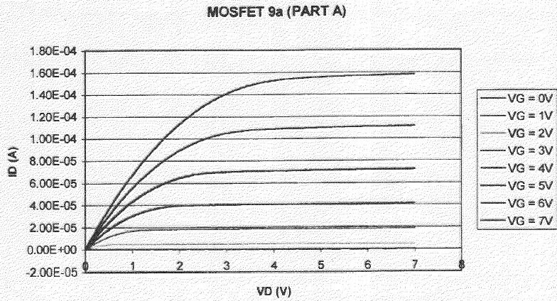
11 MOSFET I-V Characteristics For V D < V Dsat I D nw L C OX V G V T V 2 DS V DS For V D > V Dsat I D I Dsat nw 2L C OX V V 2 G T Note: V Dsat = V G - V T 11
12 Small Signal Capacitance C ( Q/V G ) C ox *p-type substrate 12
13 Typical Thin Film stress : 10 8 to 5x10 10 dynes/cm 2 (10 7 dyn/cm 2 = 1 MPa) Radius of Curvature of warpage r = E s t s 2 ( 1- ) s 6 f t f Stoney Equation 13

14 MEMS Process Flow Example: to form a hollow cantilever beam 14

15 MEMS- IC Integration Example of MEMS-first approach 15


16 Thermal Oxidation Model C G stagnant layer C s SiO 2 Si Note C s C o C o C i X 0x F 1 F 2 F 3 gas transport flux diffusion flux through SiO 2 reaction flux at interface 16
17 CVD Deposition Rate [Grove Model] film F 1 F 3 Si D k s h k G o e E kt = thickness of stagnant layer F 1 D [ C G - C S ] / F F 1 3 F 3 k S C S 17
18 C(x) C p Ion Implantation Implantation Damage 0.61 C p R p x=0 C R x p R Rp x xj 2 projected range p Cp e xr 2 R p longitudin al straggle p 2 C B Ion Channeling Si Crystal deeper penetration random scattering path 18
19 Examples: Well drive-in and S/D annealing steps T(t) Thermal ( Dt) effective Budget i ( Dt) i well drive-in step S/D Anneal step time For a complete process flow, only those steps with high Dt values are important 19
20 20
21 Depth of Focus (DOF) off point best 21
22 Normalized remianing thickness after development Photon energy dose (mj/cm2) Mormalized resist thickness Past Exam Question Positive Resist Resist cross-section after development Exposure energy dose (mj/cm2) Lateral position x ( in um) Answer Any dose < 20mJ/cm2 will work Any dose < 20mJ/cm2 will work Lateral position x ( in um) 22
23 Worst-Case Design Considerations for Etching step step height variation variation of film thickness across wafer Mask etching mask can be eroded during film etching film Substrate 23
24 Effect of RIE process variables on etching characteristics Control variable effect 24

25 Multilevel Metallization Via Interconnect
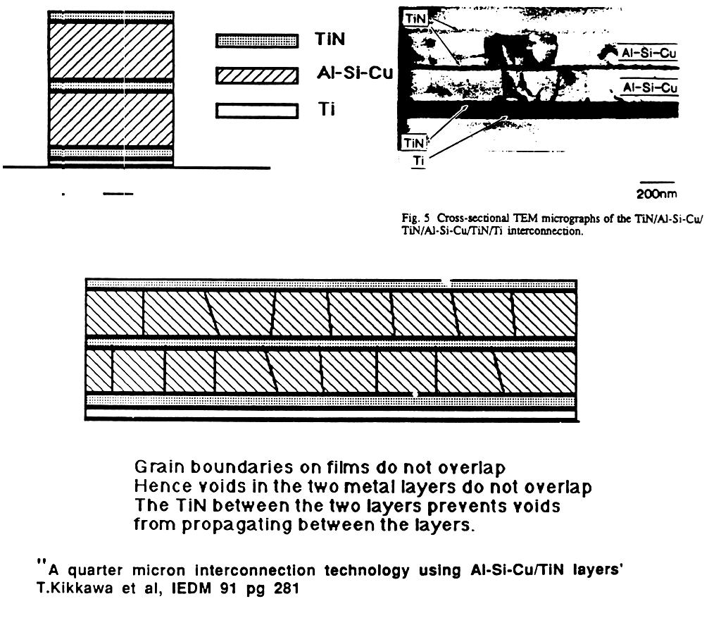
26 Electromigration Issues 26
Self-study problems and questions Processing and Device Technology, FFF110/FYSD13
 Self-study problems and questions Processing and Device Technology, FFF110/FYSD13 Version 2016_01 In addition to the problems discussed at the seminars and at the lectures, you can use this set of problems
Make sure the exam paper has 9 pages (including cover page) + 3 pages of data for reference
 + 3 pages of data for reference") UNIVERSITY OF CALIFORNIA College of Engineering Department of Electrical Engineering and Computer Sciences Spring 2006 EE143 Midterm Exam #1 Family Name First name SID Signature Make sure the exam paper
UNIVERSITY OF CALIFORNIA College of Engineering Department of Electrical Engineering and Computer Sciences Spring 2006 EE143 Midterm Exam #1 Family Name First name SID Signature Make sure the exam paper
Section 12: Intro to Devices
 Section 12: Intro to Devices Extensive reading materials on reserve, including Robert F. Pierret, Semiconductor Device Fundamentals Bond Model of Electrons and Holes Si Si Si Si Si Si Si Si Si Silicon
Section 12: Intro to Devices
 Section 12: Intro to Devices Extensive reading materials on reserve, including Robert F. Pierret, Semiconductor Device Fundamentals EE143 Ali Javey Bond Model of Electrons and Holes Si Si Si Si Si Si Si
Fabrication Technology, Part I
 EEL5225: Principles of MEMS Transducers (Fall 2004) Fabrication Technology, Part I Agenda: Microfabrication Overview Basic semiconductor devices Materials Key processes Oxidation Thin-film Deposition Reading:
Make sure the exam paper has 7 pages (including cover page) + 3 pages of data for reference
 + 3 pages of data for reference") UNIVERSITY OF CALIFORNIA College of Engineering Department of Electrical Engineering and Computer Sciences Fall 2005 EE143 Midterm Exam #1 Family Name First name SID Signature Make sure the exam paper
UNIVERSITY OF CALIFORNIA College of Engineering Department of Electrical Engineering and Computer Sciences Fall 2005 EE143 Midterm Exam #1 Family Name First name SID Signature Make sure the exam paper
EE 143 MICROFABRICATION TECHNOLOGY FALL 2014 C. Nguyen PROBLEM SET #7. Due: Friday, Oct. 24, 2014, 8:00 a.m. in the EE 143 homework box near 140 Cory
 Issued: Tuesday, Oct. 14, 2014 PROBLEM SET #7 Due: Friday, Oct. 24, 2014, 8:00 a.m. in the EE 143 homework box near 140 Cory Electroplating 1. Suppose you want to fabricate MEMS clamped-clamped beam structures
Extensive reading materials on reserve, including
 Section 12: Intro to Devices Extensive reading materials on reserve, including Robert F. Pierret, Semiconductor Device Fundamentals EE143 Ali Javey Bond Model of Electrons and Holes Si Si Si Si Si Si Si
Ion Implantation. alternative to diffusion for the introduction of dopants essentially a physical process, rather than chemical advantages:
 Ion Implantation alternative to diffusion for the introduction of dopants essentially a physical process, rather than chemical advantages: mass separation allows wide varies of dopants dose control: diffusion
Lecture 150 Basic IC Processes (10/10/01) Page ECE Analog Integrated Circuits and Systems P.E. Allen
 Page ECE Analog Integrated Circuits and Systems P.E. Allen") Lecture 150 Basic IC Processes (10/10/01) Page 1501 LECTURE 150 BASIC IC PROCESSES (READING: TextSec. 2.2) INTRODUCTION Objective The objective of this presentation is: 1.) Introduce the fabrication of
Lecture 150 Basic IC Processes (10/10/01) Page 1501 LECTURE 150 BASIC IC PROCESSES (READING: TextSec. 2.2) INTRODUCTION Objective The objective of this presentation is: 1.) Introduce the fabrication of
P. R. Nelson 1 ECE418 - VLSI. Midterm Exam. Solutions
 P. R. Nelson 1 ECE418 - VLSI Midterm Exam Solutions 1. (8 points) Draw the cross-section view for A-A. The cross-section view is as shown below.. ( points) Can you tell which of the metal1 regions is the
nmos IC Design Report Module: EEE 112
 nmos IC Design Report Author: 1302509 Zhao Ruimin Module: EEE 112 Lecturer: Date: Dr.Zhao Ce Zhou June/5/2015 Abstract This lab intended to train the experimental skills of the layout designing of the
UNIVERSITY OF CALIFORNIA. College of Engineering. Department of Electrical Engineering and Computer Sciences. Professor Ali Javey.
 UNIVERSITY OF CALIFORNIA College of Engineering Department of Electrical Engineering and Computer Sciences EE 143 Professor Ali Javey Spring 2009 Exam 2 Name: SID: Closed book. One sheet of notes is allowed.
IC Fabrication Technology
 IC Fabrication Technology * History: 1958-59: J. Kilby, Texas Instruments and R. Noyce, Fairchild * Key Idea: batch fabrication of electronic circuits n entire circuit, say 10 7 transistors and 5 levels
FLCC Seminar. Spacer Lithography for Reduced Variability in MOSFET Performance
 1 Seminar Spacer Lithography for Reduced Variability in MOSFET Performance Prof. Tsu-Jae King Liu Electrical Engineering & Computer Sciences Dept. University of California at Berkeley Graduate Student:
MOS Transistor Properties Review
 MOS Transistor Properties Review 1 VLSI Chip Manufacturing Process Photolithography: transfer of mask patterns to the chip Diffusion or ion implantation: selective doping of Si substrate Oxidation: SiO
Fig The electron mobility for a-si and poly-si TFT.
 Fig. 1-1-1 The electron mobility for a-si and poly-si TFT. Fig. 1-1-2 The aperture ratio for a-si and poly-si TFT. 33 Fig. 1-2-1 All kinds defect well. (a) is the Dirac well. (b) is the repulsive Columbic
Lecture #27. The Short Channel Effect (SCE)
") Lecture #27 ANNOUNCEMENTS Design Project: Your BJT design should meet the performance specifications to within 10% at both 300K and 360K. ( β dc > 45, f T > 18 GHz, V A > 9 V and V punchthrough > 9 V )
Lecture #27 ANNOUNCEMENTS Design Project: Your BJT design should meet the performance specifications to within 10% at both 300K and 360K. ( β dc > 45, f T > 18 GHz, V A > 9 V and V punchthrough > 9 V )
Gold Nanoparticles Floating Gate MISFET for Non-Volatile Memory Applications
 Gold Nanoparticles Floating Gate MISFET for Non-Volatile Memory Applications D. Tsoukalas, S. Kolliopoulou, P. Dimitrakis, P. Normand Institute of Microelectronics, NCSR Demokritos, Athens, Greece S. Paul,
Chapter 3 Basics Semiconductor Devices and Processing
 Chapter 3 Basics Semiconductor Devices and Processing Hong Xiao, Ph. D. www2.austin.cc.tx.us/hongxiao/book.htm Hong Xiao, Ph. D. www2.austin.cc.tx.us/hongxiao/book.htm 1 Objectives Identify at least two
EE C247B / ME C218 INTRODUCTION TO MEMS DESIGN SPRING 2016 C. NGUYEN PROBLEM SET #4
 Issued: Wednesday, March 4, 2016 PROBLEM SET #4 Due: Monday, March 14, 2016, 8:00 a.m. in the EE C247B homework box near 125 Cory. 1. This problem considers bending of a simple cantilever and several methods
3.155J/6.152J Microelectronic Processing Technology Fall Term, 2004
 3.155J/6.152J Microelectronic Processing Technology Fall Term, 2004 Bob O'Handley Martin Schmidt Quiz Nov. 17, 2004 Ion implantation, diffusion [15] 1. a) Two identical p-type Si wafers (N a = 10 17 cm
ECE 342 Electronic Circuits. Lecture 6 MOS Transistors
 ECE 342 Electronic Circuits Lecture 6 MOS Transistors Jose E. Schutt-Aine Electrical & Computer Engineering University of Illinois jesa@illinois.edu 1 NMOS Transistor Typically L = 0.1 to 3 m, W = 0.2
Lecture 12: MOS Capacitors, transistors. Context
 Lecture 12: MOS Capacitors, transistors Context In the last lecture, we discussed PN diodes, and the depletion layer into semiconductor surfaces. Small signal models In this lecture, we will apply those
Make sure the exam paper has 8 pages plus an appendix page at the end.
 UNIVERSITY OF CALIFORNIA College of Engineering Deartment of Electrical Engineering and Comuter Sciences Fall 2000 EE143 Midterm Exam #1 Family Name First name Signature Make sure the exam aer has 8 ages
EE 212 FALL ION IMPLANTATION - Chapter 8 Basic Concepts
 EE 212 FALL 1999-00 ION IMPLANTATION - Chapter 8 Basic Concepts Ion implantation is the dominant method of doping used today. In spite of creating enormous lattice damage it is favored because: Large range
Section 7: Diffusion. Jaeger Chapter 4. EE143 Ali Javey
 Section 7: Diffusion Jaeger Chapter 4 Surface Diffusion: Dopant Sources (a) Gas Source: AsH 3, PH 3, B 2 H 6 (b) Solid Source BN Si BN Si (c) Spin-on-glass SiO 2 +dopant oxide (d) Liquid Source. Fick s
Microelectronics Part 1: Main CMOS circuits design rules
 GBM8320 Dispositifs Médicaux telligents Microelectronics Part 1: Main CMOS circuits design rules Mohamad Sawan et al. Laboratoire de neurotechnologies Polystim! http://www.cours.polymtl.ca/gbm8320/! med-amine.miled@polymtl.ca!
Electrical Characteristics of MOS Devices
 Electrical Characteristics of MOS Devices The MOS Capacitor Voltage components Accumulation, Depletion, Inversion Modes Effect of channel bias and substrate bias Effect of gate oide charges Threshold-voltage
Lecture 0: Introduction
 Lecture 0: Introduction Introduction q Integrated circuits: many transistors on one chip q Very Large Scale Integration (VLSI): bucketloads! q Complementary Metal Oxide Semiconductor Fast, cheap, low power
EE141- Spring 2003 Lecture 3. Last Lecture
 - Spring 003 Lecture 3 IC Manufacturing 1 Last Lecture Design Metrics (part 1) Today Design metrics (wrap-up) IC manufacturing 1 Administrivia Discussion sessions start this week. Only one this week (Dejan
MOSFET: Introduction
 E&CE 437 Integrated VLSI Systems MOS Transistor 1 of 30 MOSFET: Introduction Metal oxide semiconductor field effect transistor (MOSFET) or MOS is widely used for implementing digital designs Its major
Scaling Issues in Planar FET: Dual Gate FET and FinFETs
 Scaling Issues in Planar FET: Dual Gate FET and FinFETs Lecture 12 Dr. Amr Bayoumi Fall 2014 Advanced Devices (EC760) Arab Academy for Science and Technology - Cairo 1 Outline Scaling Issues for Planar
UNIVERSITY OF CALIFORNIA College of Engineering Department of Electrical Engineering and Computer Sciences. EECS 130 Professor Ali Javey Fall 2006
 UNIVERSITY OF CALIFORNIA College of Engineering Department of Electrical Engineering and Computer Sciences EECS 130 Professor Ali Javey Fall 2006 Midterm 2 Name: SID: Closed book. Two sheets of notes are
Dopant Diffusion. (1) Predeposition dopant gas. (2) Drive-in Turn off dopant gas. dose control. Doped Si region
 Predeposition dopant gas. (2) Drive-in Turn off dopant gas. dose control. Doped Si region") Dopant Diffusion (1) Predeposition dopant gas dose control SiO Si SiO Doped Si region () Drive-in Turn off dopant gas or seal surface with oxide profile control (junction depth; concentration) SiO SiO
Dopant Diffusion (1) Predeposition dopant gas dose control SiO Si SiO Doped Si region () Drive-in Turn off dopant gas or seal surface with oxide profile control (junction depth; concentration) SiO SiO
ESE 570: Digital Integrated Circuits and VLSI Fundamentals
 ESE 570: Digital Integrated Circuits and VLSI Fundamentals Lec 4: January 23, 2018 MOS Transistor Theory, MOS Model Penn ESE 570 Spring 2018 Khanna Lecture Outline! CMOS Process Enhancements! Semiconductor
The Devices. Digital Integrated Circuits A Design Perspective. Jan M. Rabaey Anantha Chandrakasan Borivoje Nikolic. July 30, 2002
 Digital Integrated Circuits A Design Perspective Jan M. Rabaey Anantha Chandrakasan Borivoje Nikolic The Devices July 30, 2002 Goal of this chapter Present intuitive understanding of device operation Introduction
EE-612: Lecture 22: CMOS Process Steps
 EE-612: Lecture 22: CMOS Process Steps Mark Lundstrom Electrical and Computer Engineering Purdue University West Lafayette, IN USA Fall 2006 NCN www.nanohub.org Lundstrom EE-612 F06 1 outline 1) Unit Process
ESE 570: Digital Integrated Circuits and VLSI Fundamentals
 ESE 570: Digital Integrated Circuits and VLSI Fundamentals Lec 4: January 29, 2019 MOS Transistor Theory, MOS Model Penn ESE 570 Spring 2019 Khanna Lecture Outline! CMOS Process Enhancements! Semiconductor
CMPEN 411 VLSI Digital Circuits. Lecture 03: MOS Transistor
 CMPEN 411 VLSI Digital Circuits Lecture 03: MOS Transistor Kyusun Choi [Adapted from Rabaey s Digital Integrated Circuits, Second Edition, 2003 J. Rabaey, A. Chandrakasan, B. Nikolic] CMPEN 411 L03 S.1
L ECE 4211 UConn F. Jain Scaling Laws for NanoFETs Chapter 10 Logic Gate Scaling
 L13 04202017 ECE 4211 UConn F. Jain Scaling Laws for NanoFETs Chapter 10 Logic Gate Scaling Scaling laws: Generalized scaling (GS) p. 610 Design steps p.613 Nanotransistor issues (page 626) Degradation
SECTION: Circle one: Alam Lundstrom. ECE 305 Exam 5 SOLUTIONS: Spring 2016 April 18, 2016 M. A. Alam and M.S. Lundstrom Purdue University
 NAME: PUID: SECTION: Circle one: Alam Lundstrom ECE 305 Exam 5 SOLUTIONS: April 18, 2016 M A Alam and MS Lundstrom Purdue University This is a closed book exam You may use a calculator and the formula
EE143 Fall 2016 Microfabrication Technologies. Lecture 6: Thin Film Deposition Reading: Jaeger Chapter 6
 EE143 Fall 2016 Microfabrication Technologies Lecture 6: Thin Film Deposition Reading: Jaeger Chapter 6 Prof. Ming C. Wu wu@eecs.berkeley.edu 511 Sutardja Dai Hall (SDH) 1 Vacuum Basics Units 1 atmosphere
UNIVERSITY OF CALIFORNIA College of Engineering Department of Electrical Engineering and Computer Sciences. Fall Exam 1
 UNIVERSITY OF CALIFORNIA College of Engineering Department of Electrical Engineering and Computer Sciences EECS 143 Fall 2008 Exam 1 Professor Ali Javey Answer Key Name: SID: 1337 Closed book. One sheet
LECTURE 3 MOSFETS II. MOS SCALING What is Scaling?
 LECTURE 3 MOSFETS II Lecture 3 Goals* * Understand constant field and constant voltage scaling and their effects. Understand small geometry effects for MOS transistors and their implications modeling and
6.152J / 3.155J Spring 05 Lecture 08-- IC Lab Testing. IC Lab Testing. Outline. Structures to be Characterized. Sheet Resistance, N-square Resistor
 IC Lab Testing Review Process Outline Structures to be Characterized Resistors Sheet Resistance, Nsquare Resistor MOS Capacitors Flatband Voltage, Threshold Voltage, Oxide Thickness, Oxide Charges, Substrate
UNIVERSITY OF CALIFORNIA College of Engineering Department of Electrical Engineering and Computer Sciences. Professor Chenming Hu.
 UNIVERSITY OF CALIFORNIA College of Engineering Department of Electrical Engineering and Computer Sciences EECS 130 Spring 2009 Professor Chenming Hu Midterm I Name: Closed book. One sheet of notes is
UNIVERSITY OF CALIFORNIA College of Engineering Department of Electrical Engineering and Computer Sciences. Professor Oldham Fall 1999
 UNIVERSITY OF CLIFORNI College of Engineering Department of Electrical Engineering and Computer Sciences Professor Oldham Fall 1999 EECS 40 FINL EXM 13 December 1999 Name: Last, First Student ID: T: Kusuma
ELEN0037 Microelectronic IC Design. Prof. Dr. Michael Kraft
 ELEN0037 Microelectronic IC Design Prof. Dr. Michael Kraft Lecture 2: Technological Aspects Technology Passive components Active components CMOS Process Basic Layout Scaling CMOS Technology Integrated
Ion Implantation ECE723
 Ion Implantation Topic covered: Process and Advantages of Ion Implantation Ion Distribution and Removal of Lattice Damage Simulation of Ion Implantation Range of Implanted Ions Ion Implantation is the
ABSTRACT I NTRODUCT ION
 DESIGN OF AN ION IMPLANTATION PROCESS MONITORING CHIP ON I.C.E. AND PROVIDE A METHODOLOGY FOR EVALUATION OF TESTING RESULTS. by JOSEPH J. BURKIS 5th YEAR MiCROELECTRONIC STUDENT ROCHESTER INSTITUTE OF
Section 6: Ion Implantation. Jaeger Chapter 5
 Section 6: Ion Imlantation Jaeger Chater 5 Ion Imlantation - Overview Wafer is Target in High Energy Accelerator Imurities Shot into Wafer Preferred Method of Adding Imurities to Wafers Wide Range of Imurity
EE115C Winter 2017 Digital Electronic Circuits. Lecture 3: MOS RC Model, CMOS Manufacturing
 EE115C Winter 2017 Digital Electronic Circuits Lecture 3: MOS RC Model, CMOS Manufacturing Agenda MOS Transistor: RC Model (pp. 104-113) S R on D CMOS Manufacturing Process (pp. 36-46) S S C GS G G C GD
EE 434 Lecture 12. Process Flow (wrap up) Device Modeling in Semiconductor Processes
 Device Modeling in Semiconductor Processes") EE 434 Lecture 12 Process Flow (wrap up) Device Modeling in Semiconductor Processes Quiz 6 How have process engineers configured a process to assure that the thickness of the gate oxide for the p-channel
EE 434 Lecture 12 Process Flow (wrap up) Device Modeling in Semiconductor Processes Quiz 6 How have process engineers configured a process to assure that the thickness of the gate oxide for the p-channel
Chapter 2. Design and Fabrication of VLSI Devices
 Chapter 2 Design and Fabrication of VLSI Devices Jason Cong 1 Design and Fabrication of VLSI Devices Objectives: To study the materials used in fabrication of VLSI devices. To study the structure of devices
EE 434 Lecture 7. Process Technology
 EE 434 Lecture 7 Process Technology Quiz 4 How many wafers can be obtained from a 2m pull? Neglect the material wasted in the kerf used to separate the wafers. 2m And the number is. 1 8 3 5 6 4 9 7 2 1
Lecture 6 PN Junction and MOS Electrostatics(III) Metal-Oxide-Semiconductor Structure
 Metal-Oxide-Semiconductor Structure") Lecture 6 PN Junction and MOS Electrostatics(III) Metal-Oxide-Semiconductor Structure Outline 1. Introduction to MOS structure 2. Electrostatics of MOS in thermal equilibrium 3. Electrostatics of MOS with
Lecture 6 PN Junction and MOS Electrostatics(III) Metal-Oxide-Semiconductor Structure Outline 1. Introduction to MOS structure 2. Electrostatics of MOS in thermal equilibrium 3. Electrostatics of MOS with
Choice of V t and Gate Doping Type
 Choice of V t and Gate Doping Type To make circuit design easier, it is routine to set V t at a small positive value, e.g., 0.4 V, so that, at V g = 0, the transistor does not have an inversion layer and
Dopant Diffusion Sources
 Dopant Diffusion (1) Predeposition dopant gas dose control SiO Si SiO Doped Si region () Drive-in Turn off dopant gas or seal surface with oide profile control (junction depth; concentration) SiO SiO Si
Impact of parametric mismatch and fluctuations on performance and yield of deep-submicron CMOS technologies. Philips Research, The Netherlands
 Impact of parametric mismatch and fluctuations on performance and yield of deep-submicron CMOS technologies Hans Tuinhout, The Netherlands motivation: from deep submicron digital ULSI parametric spread
ION IMPLANTATION - Chapter 8 Basic Concepts
 ION IMPLANTATION - Chapter 8 Basic Concepts Ion implantation is the dominant method of doping used today. In spite of creating enormous lattice damage it is favored because: Large range of doses - 1 11
Today s lecture. EE141- Spring 2003 Lecture 4. Design Rules CMOS Inverter MOS Transistor Model
 - Spring 003 Lecture 4 Design Rules CMOS Inverter MOS Transistor Model Today s lecture Design Rules The CMOS inverter at a glance An MOS transistor model for manual analysis Important! Labs start next
EE 5211 Analog Integrated Circuit Design. Hua Tang Fall 2012
 EE 5211 Analog Integrated Circuit Design Hua Tang Fall 2012 Today s topic: 1. Introduction to Analog IC 2. IC Manufacturing (Chapter 2) Introduction What is Integrated Circuit (IC) vs discrete circuits?
EE105 - Fall 2006 Microelectronic Devices and Circuits
 EE105 - Fall 2006 Microelectronic Devices and Circuits Prof. Jan M. Rabaey (jan@eecs) Lecture 7: MOS Transistor Some Administrative Issues Lab 2 this week Hw 2 due on We Hw 3 will be posted same day MIDTERM
! CMOS Process Enhancements. ! Semiconductor Physics. " Band gaps. " Field Effects. ! MOS Physics. " Cut-off. " Depletion.
 ESE 570: Digital Integrated Circuits and VLSI Fundamentals Lec 4: January 9, 019 MOS Transistor Theory, MOS Model Lecture Outline CMOS Process Enhancements Semiconductor Physics Band gaps Field Effects
4FNJDPOEVDUPS 'BCSJDBUJPO &UDI
 2010.5.4 1 Major Fabrication Steps in CMOS Process Flow UV light oxygen Silicon dioxide Silicon substrate Oxidation (Field oxide) photoresist Photoresist Coating Mask exposed photoresist Mask-Wafer Exposed
Lecture 15 OUTLINE. MOSFET structure & operation (qualitative) Review of electrostatics The (N)MOS capacitor
 Review of electrostatics The (N)MOS capacitor") Lecture 15 OUTLINE MOSFET structure & operation (qualitative) Review of electrostatics The (N)MOS capacitor Electrostatics t ti Charge vs. voltage characteristic Reading: Chapter 6.1 6.2.1 EE105 Fall 2007
Lecture 15 OUTLINE MOSFET structure & operation (qualitative) Review of electrostatics The (N)MOS capacitor Electrostatics t ti Charge vs. voltage characteristic Reading: Chapter 6.1 6.2.1 EE105 Fall 2007
Properties of Error Function erf(z) And Complementary Error Function erfc(z)
 And Complementary Error Function erfc(z)") Properties of Error Function erf(z) And Complementary Error Function erfc(z) z erf (z) π e -y dy erfc (z) 1 - erf (z) erf () erf( ) 1 erf(- ) - 1 erf (z) d erf(z) dz π z for z
Properties of Error Function erf(z) And Complementary Error Function erfc(z) z erf (z) π e -y dy erfc (z) 1 - erf (z) erf () erf( ) 1 erf(- ) - 1 erf (z) d erf(z) dz π z for z
Final Examination EE 130 December 16, 1997 Time allotted: 180 minutes
 Final Examination EE 130 December 16, 1997 Time allotted: 180 minutes Problem 1: Semiconductor Fundamentals [30 points] A uniformly doped silicon sample of length 100µm and cross-sectional area 100µm 2
There's Plenty of Room at the Bottom
 There's Plenty of Room at the Bottom 12/29/1959 Feynman asked why not put the entire Encyclopedia Britannica (24 volumes) on a pin head (requires atomic scale recording). He proposed to use electron microscope
Lecture 11: MOS Transistor
 Lecture 11: MOS Transistor Prof. Niknejad Lecture Outline Review: MOS Capacitors Regions MOS Capacitors (3.8 3.9) CV Curve Threshold Voltage MOS Transistors (4.1 4.3): Overview Cross-section and layout
EE C245 ME C218 Introduction to MEMS Design Fall 2007
 EE C245 ME C218 Introduction to MEMS Design Fall 2007 Prof. Clark T.-C. Nguyen Dept. of Electrical Engineering & Computer Sciences University of California at Berkeley Berkeley, CA 94720 Lecture 12: Mechanics
Chapter 2 Process Variability. Overview. 2.1 Sources and Types of Variations
 Chapter 2 Process Variability Overview Parameter variability has always been an issue in integrated circuits. However, comparing with the size of devices, it is relatively increasing with technology evolution,
MOS CAPACITOR AND MOSFET
 EE336 Semiconductor Devices 1 MOS CAPACITOR AND MOSFET Dr. Mohammed M. Farag Ideal MOS Capacitor Semiconductor Devices Physics and Technology Chapter 5 EE336 Semiconductor Devices 2 MOS Capacitor Structure
Film Deposition Part 1
 1 Film Deposition Part 1 Chapter 11 : Semiconductor Manufacturing Technology by M. Quirk & J. Serda Spring Semester 2013 Saroj Kumar Patra Semidonductor Manufacturing Technology, Norwegian University of
EE410 vs. Advanced CMOS Structures
 EE410 vs. Advanced CMOS Structures Prof. Krishna S Department of Electrical Engineering S 1 EE410 CMOS Structure P + poly-si N + poly-si Al/Si alloy LPCVD PSG P + P + N + N + PMOS N-substrate NMOS P-well
Semiconductor Devices. C. Hu: Modern Semiconductor Devices for Integrated Circuits Chapter 5
 Semiconductor Devices C. Hu: Modern Semiconductor Devices for Integrated Circuits Chapter 5 Global leader in environmental and industrial measurement Wednesday 3.2. afternoon Tour around facilities & lecture
! CMOS Process Enhancements. ! Semiconductor Physics. " Band gaps. " Field Effects. ! MOS Physics. " Cut-off. " Depletion.
 ESE 570: Digital Integrated Circuits and VLSI Fundamentals Lec 4: January 3, 018 MOS Transistor Theory, MOS Model Lecture Outline! CMOS Process Enhancements! Semiconductor Physics " Band gaps " Field Effects!
EE105 - Fall 2005 Microelectronic Devices and Circuits
 EE105 - Fall 005 Microelectronic Devices and Circuits ecture 7 MOS Transistor Announcements Homework 3, due today Homework 4 due next week ab this week Reading: Chapter 4 1 ecture Material ast lecture
Part 4: Heterojunctions - MOS Devices. MOSFET Current Voltage Characteristics
 MOS Device Uses: Part 4: Heterojunctions - MOS Devices MOSCAP capacitor: storing charge, charge-coupled device (CCD), etc. MOSFET transistor: switch, current amplifier, dynamic random access memory (DRAM-volatile),
MSE 310/ECE 340: Electrical Properties of Materials Fall 2014 Department of Materials Science and Engineering Boise State University
 MSE 310/ECE 340: Electrical Properties of Materials Fall 2014 Department of Materials Science and Engineering Boise State University Practice Final Exam 1 Read the questions carefully Label all figures
Semiconductor Integrated Process Design (MS 635)
") Semiconductor Integrated Process Design (MS 635) Instructor: Prof. Keon Jae Lee - Office: 응용공학동 #4306, Tel: #3343 - Email: keonlee@kaist.ac.kr Lecture: (Tu, Th), 1:00-2:15 #2425 Office hour: Tues & Thur
Semiconductor Integrated Process Design (MS 635) Instructor: Prof. Keon Jae Lee - Office: 응용공학동 #4306, Tel: #3343 - Email: keonlee@kaist.ac.kr Lecture: (Tu, Th), 1:00-2:15 #2425 Office hour: Tues & Thur
ECE 305 Exam 5 SOLUTIONS: Spring 2015 April 17, 2015 Mark Lundstrom Purdue University
 NAME: PUID: : ECE 305 Exam 5 SOLUTIONS: April 17, 2015 Mark Lundstrom Purdue University This is a closed book exam. You may use a calculator and the formula sheet at the end of this exam. Following the
Lecture 15 OUTLINE. MOSFET structure & operation (qualitative) Review of electrostatics The (N)MOS capacitor
 Review of electrostatics The (N)MOS capacitor") Lecture 15 OUTLINE MOSFET structure & operation (qualitative) Review of electrostatics The (N)MOS capacitor Electrostatics Charge vs. voltage characteristic Reading: Chapter 6.1 6.2.1 EE15 Spring 28 Lecture
Lecture 15 OUTLINE MOSFET structure & operation (qualitative) Review of electrostatics The (N)MOS capacitor Electrostatics Charge vs. voltage characteristic Reading: Chapter 6.1 6.2.1 EE15 Spring 28 Lecture
Regents of the University of California
 Deep Reactive-Ion Etching (DRIE) DRIE Issues: Etch Rate Variance The Bosch process: Inductively-coupled plasma Etch Rate: 1.5-4 μm/min Two main cycles in the etch: Etch cycle (5-15 s): SF 6 (SF x+ ) etches
Electric-Field Induced F - Migration in Self-Aligned InGaAs MOSFETs and Mitigation
 Electric-Field Induced F - Migration in Self-Aligned InGaAs MOSFETs and Mitigation X. Cai, J. Lin, D. A. Antoniadis and J. A. del Alamo Microsystems Technology Laboratories, MIT December 5, 2016 Sponsors:
Objective: Competitive Low-Cost Thin-Film Varactor Technology. Integrated Monolithic Capacitors using Sputtered/MOCVD material on low-cost substrates
 Overview of Program Objective: Competitive Low-Cost Thin-Film Varactor Technology coplanar waveguide (CPW) capacitor ground signal ground Si substrate etched troughs Focus of Our Program! Reproducibility!
JFET/MESFET. JFET: small gate current (reverse leakage of the gate-to-channel junction) More gate leakage than MOSFET, less than bipolar.
 More gate leakage than MOSFET, less than bipolar.") JFET/MESFET JFET: small gate current (reverse leakage of the gate-to-channel junction) More gate leakage than MOSFET, less than bipolar. JFET has higher transconductance than the MOSFET. Used in low-noise,
JFET/MESFET JFET: small gate current (reverse leakage of the gate-to-channel junction) More gate leakage than MOSFET, less than bipolar. JFET has higher transconductance than the MOSFET. Used in low-noise,
MENA9510 characterization course: Capacitance-voltage (CV) measurements
 measurements") MENA9510 characterization course: Capacitance-voltage (CV) measurements 30.10.2017 Halvard Haug Outline Overview of interesting sample structures Ohmic and schottky contacts Why C-V for solar cells? The
MENA9510 characterization course: Capacitance-voltage (CV) measurements 30.10.2017 Halvard Haug Outline Overview of interesting sample structures Ohmic and schottky contacts Why C-V for solar cells? The
Circuits. L5: Fabrication and Layout -2 ( ) B. Mazhari Dept. of EE, IIT Kanpur. B. Mazhari, IITK. G-Number
 B. Mazhari Dept. of EE, IIT Kanpur. B. Mazhari, IITK. G-Number") EE610: CMOS Analog Circuits L5: Fabrication and Layout -2 (12.8.2013) B. Mazhari Dept. of EE, IIT Kanpur 44 Passive Components: Resistor Besides MOS transistors, sometimes one requires to implement passive
EE610: CMOS Analog Circuits L5: Fabrication and Layout -2 (12.8.2013) B. Mazhari Dept. of EE, IIT Kanpur 44 Passive Components: Resistor Besides MOS transistors, sometimes one requires to implement passive
Changing the Dopant Concentration. Diffusion Doping Ion Implantation
 Changing the Dopant Concentration Diffusion Doping Ion Implantation Step 11 The photoresist is removed with solvent leaving a ridge of polysilicon (the transistor's gate), which rises above the silicon
EE 330 Lecture 16. MOS Device Modeling p-channel n-channel comparisons Model consistency and relationships CMOS Process Flow
 EE 330 Lecture 16 MOS Device Modeling p-channel n-channel comparisons Model consistency and relationships CMOS Process Flow Review from Last Time Operation Regions by Applications Id I D 300 250 200 150
A 20 nm gate-length ultra-thin body p-mosfet with silicide source/drain
 Superlattices and Microstructures, Vol. 28, No. 5/6, 2000 doi:10.1006/spmi.2000.0947 Available online at http://www.idealibrary.com on A 20 nm gate-length ultra-thin body p-mosfet with silicide source/drain
Semiconductor Physics Problems 2015
 Semiconductor Physics Problems 2015 Page and figure numbers refer to Semiconductor Devices Physics and Technology, 3rd edition, by SM Sze and M-K Lee 1. The purest semiconductor crystals it is possible
Lecture 020 Review of CMOS Technology (09/01/03) Page 020-1
 Page 020-1") Lecture 020 Review of CMOS Technology (09/01/03) Page 020-1 LECTURE 020 REVIEW OF CMOS TECHNOLOGY INTRODUCTION Objective Provide sufficient background to understand the limits and capabilities of CMOS
Lecture 020 Review of CMOS Technology (09/01/03) Page 020-1 LECTURE 020 REVIEW OF CMOS TECHNOLOGY INTRODUCTION Objective Provide sufficient background to understand the limits and capabilities of CMOS
September 21, 2005, Wednesday
 , Wednesday Doping and diffusion I Faster MOSFET requires shorter channel P + Poly Al Al Motivation Requires shallower source, drain Al P + Poly Al source drain Shorter channel length; yes, but same source
Ion Implant Part 1. Saroj Kumar Patra, TFE4180 Semiconductor Manufacturing Technology. Norwegian University of Science and Technology ( NTNU )
") 1 Ion Implant Part 1 Chapter 17: Semiconductor Manufacturing Technology by M. Quirk & J. Serda Spring Semester 2014 Saroj Kumar Patra,, Norwegian University of Science and Technology ( NTNU ) 2 Objectives
1 Ion Implant Part 1 Chapter 17: Semiconductor Manufacturing Technology by M. Quirk & J. Serda Spring Semester 2014 Saroj Kumar Patra,, Norwegian University of Science and Technology ( NTNU ) 2 Objectives
EE 330 Lecture 16. MOSFET Modeling CMOS Process Flow
 EE 330 Lecture 16 MOSFET Modeling CMOS Process Flow Model Extensions 300 Id 250 200 150 100 50 300 0 0 1 2 3 4 5 Vds Existing Model 250 200 Id 150 100 50 Slope is not 0 0 0 1 2 3 4 Actual Device Vds Model
DIFFUSION - Chapter 7
 DIFFUSION - Chapter 7 Doping profiles determine many short-channel characteristics in MOS devices. Resistance impacts drive current. Scaling implies all lateral and vertical dimensions scale by the same
EECS240 Spring Today s Lecture. Lecture 2: CMOS Technology and Passive Devices. Lingkai Kong EECS. EE240 CMOS Technology
 EECS240 Spring 2013 Lecture 2: CMOS Technology and Passive Devices Lingkai Kong EECS Today s Lecture EE240 CMOS Technology Passive devices Motivation Resistors Capacitors (Inductors) Next time: MOS transistor