Micro- and Nano-Technology... for Optics
|
|
|
- Scarlett Davidson
- 5 years ago
- Views:
Transcription


1 Micro- and Nano-Technology for Optics U.D. Zeitner Fraunhofer Institut für Angewandte Optik und Feinmechanik Jena Today: 1. Introduction E. Bernhard Kley Institute of Applied Physics Friedrich-Schiller University Jena and Fraunhofer Institut für Angewandte Optik und Feinmechanik Jena
2 Course Content 1. Introduction (today) 2. Basic optical considerations - discussion of physical effects relevant in micro- and nano-optics 3. Fabrication technologies for micro- and nano-structures - Coating technologies - Lithography - Etching technologies - Replication - Ultra-precision micro-machining 4. Characterization techniques - mechanical profiler - AFM - SEM - optical surface profiler - interferometer 5. Applications
3 Additional Information Literature: - S. Sinzinger, J. Jahns Microoptics, Wiley-VCH - H.-P. Herzig Micro-Optics, Taylor & Francis - B.C. Kress, P. Meyrueis Applied Digital Optics, Wiley - C. Mack Fundamental Principles of Optical Lithography, Wiley Course material will be uploaded to: Lecture Micro- and Nano-Technology


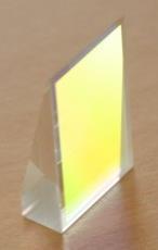
4 Micro-Structured Optics in Nature 100µm Lens-arrays as insects eyes 2µm Nano-structures with anti-reflection properties on moth seyes 4µm Colors of butterflies by diffraction gratings

5 Different Approaches Nature Technology!? Bottom-Up Top-Down Lithography
6 Modern and high end optics need micro- und nanostructures 2 prominent examples

7 Vigo Galaxy cluster About 150 galaxies visible in the picture Galaxies are very different and what about our milky way?


8 GAIA s effective medium grating 230mm RVS GAIA (ESA) launched in Dec NGC 6744
 -1E9 Stars - Magnitude: 22.")

9 Spectrometer grating for the Gaia mission of European Space Agency Gaia (Dec. 2011) -1E9 Stars - Magnitude: Distance measurement by read shift measurement Radial Velocity Spectrometer Spektral range: nm Grating

![of Relativity [Einstein, AdP 1916]](/docs-images/82/86061251/images/10-2.jpg "relative length deviation: [www.")
10 Gravitational Waves Gravitational wave Astronomy 1916 General Theory of Relativity [Einstein, AdP 1916] relative length deviation: [
11 Gravitational Wave Detection Reflective Michelson-Interferometer and critical components How to reduce the thermas noise Dl Detector [Drever, Proc. 7th M. Grossmann Meeting 1996


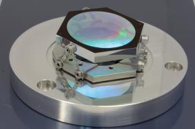
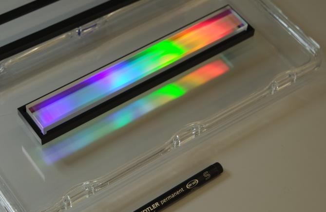
12 Monolithic dielectric mirror Motivation: Cavities for interferometer in gravitational detection and lasers Low optical and mechanical loss is required high reflectivity low mechanical Q-factor high mechanical Q-factor low reflectivity quartz / silicon n H n L n H n L n H n L n H Does a monolithic solution exist?
 waveguide + grating")

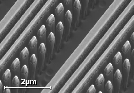
13 Monolithic resonant Si-mirror ( =1550 nm) waveguide + grating grating/effective media Si Si 99.8% reflectivity 1550nm
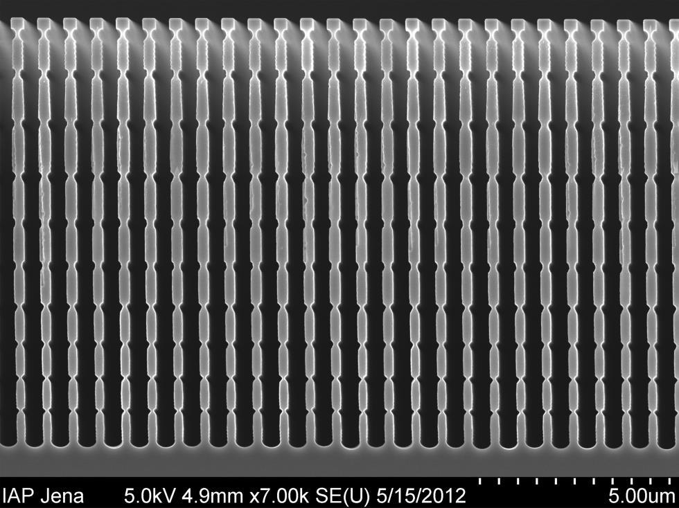
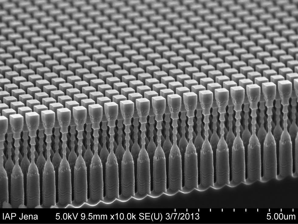
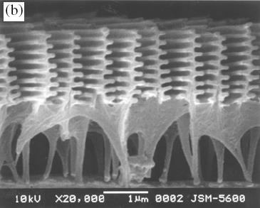
14 Silicon-Pattern for Monolithic Mirrors

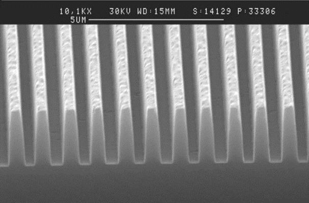
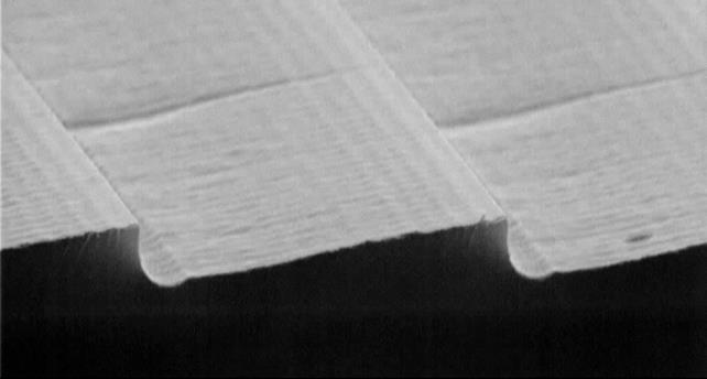
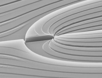
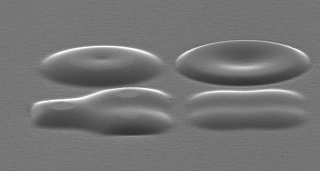
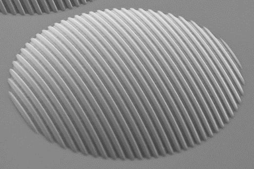
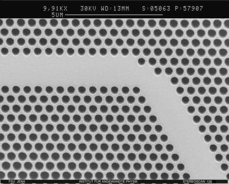
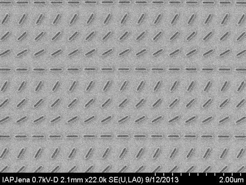
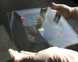
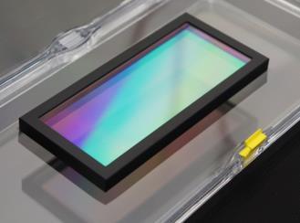
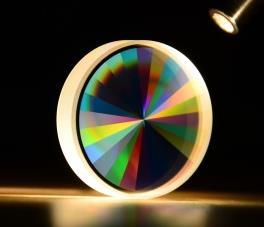
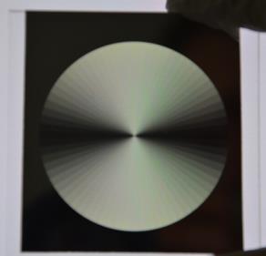
15 Examples of micro-structured elements huge variety of low and high resolution structures


16 Size scale of micro-optical effects characteristic feature size 1mm micro-lenses, micro-prisms hybride elements 100µm 10µm 1µm 100nm 10nm lens-arrays, refractive beam-shaper diffractive beam-shaper, Fresnel-lenses, diffraction gratings effective media, sub- -gratings, photonic crystals, meta-materials
17 micro optics Size-Scale of Optical Structures optical effects 1m astronomic mirrors optical elements law of refraction and reflection 1mm lenses miniaturized lenses micro-lenses paraxial beam splitters light diffraction effective medium 1µm antireflection pattern, polarizers, phase retarder photonic crystals spectroscopic gratings non paraxial beam splitter spontaneous and stimulated emission 1nm 1Å (atomic size) light sources


18 Effects of Size-Scaling focus: f=5mm 125µm diffractive beam splitter wiregridpolarizer artificial dichroitic materials 2µm structure size 1mm 100µm 10µm 1µm 100nm physical effect: refraction diffraction disturbing useful! effective materialproperties influence of physical effects on optical functions is changing if characteristic feature sizes are scaled
19 Milestones of optical engineering Fourier Fourier expansion Maxwell electromagnetic wave theory Hertz exp. confirm. of Maxwell Personal Computer Fundamental understanding of optics Basics in physics and mathematics Analytical and numerical evaluation of physical optics Fresnel wave theory of the light Abbe theory of opt. image Zuse st calculator Dedicated micro- and nanomachining technologies
20 Fabrication Technologies for Micro-Optics different size and functionality different fabrication methods for micro-optical components compared to classical (macro) optics common micro-optics fabrication methods are lithography (photo-, e-beam-, laser-) ultra precision micro-machining melting / reflow technology more elaborated technologies
21 Lithography Process Chain for Resist pattern 1. Substrate preparation (cleaning, ) 2. Resist coating (e.g. spin coating) 3. Baking 4. Resist exposure e-beam lithography or photolithography 5. Resist development, e - Substrate (e.g. Si-wafer) resist (sensitive to light or electrons) evaporation of solvent patterned resist mask for subsequent processes


22 High-End Lithography Tool microelectronic chips on Si-wafers DUV lithography stepper, =193nm (ASML) EUV lithography stepper, =13.5nm (ASML) very low flexibility


23 Lithography Roadmap (past development) 2010 lithography roadmap
24 Lithography Roadmap (ongoing) International Technology Roadmap for Semiconductors (2015)
25 Lithography for Optical Applications Lithography tools are developed for micro-electronics fabrication! steady development along semiconductor road-map vanishing versatility for other applications Demands of optics on lithography: arbitrary lateral contours (often radially symmetric) several 100mm size of single elements with sub-micron features thick substrates for elements with low wave-front error non-planar substrates possible


26 Typical Optical Surfaces and Contours Contours Profiles lens prism beam shaper characteristic detail >> binary grating blazed grating > subwavelength gratings < complex surface profiles >> > < Courtesy of E.-B. Kley

27 Demanding Micro Optics Applications Pulse compression gratings Computer-Generated Holograms Spectrometry for Space Applications Polarizers
28 Lithography Process Chain for Optics e - 1. Resist exposure with e-beam lithography resist Cr-layer SiO 2 -Substrate 2. Resist development 3. Chromium etching (RIE) 4. Deep etching into substrate (ICP) optional: multiple iterations of the process for multi-level elements
29 Technology for continuous profiles variable dose exposure: intensity modulated exposure beam proportional transfer (RIE): Ions (e.g. CF 4 ) resist substrate development: t 1 t 2 dose dependent profile depth in resist after development process element profile transferred into substrate material
Lecture 23 Optical MEMS (5)
") EEL6935 Advanced MEMS (Spring 2005) Instructor: Dr. Huikai Xie Lecture 23 Optical MEMS (5) Agenda: Microlenses Diffractive Microgratings Example Devices Reference: S. Sinzinger and J. Jahns, Chapter 6
EEL6935 Advanced MEMS (Spring 2005) Instructor: Dr. Huikai Xie Lecture 23 Optical MEMS (5) Agenda: Microlenses Diffractive Microgratings Example Devices Reference: S. Sinzinger and J. Jahns, Chapter 6
PRINCIPLES OF PHYSICAL OPTICS
 PRINCIPLES OF PHYSICAL OPTICS C. A. Bennett University of North Carolina At Asheville WILEY- INTERSCIENCE A JOHN WILEY & SONS, INC., PUBLICATION CONTENTS Preface 1 The Physics of Waves 1 1.1 Introduction
Fabrication of micro-optical components in polymer using proton beam micro-machining and modification
 Nuclear Instruments and Methods in Physics Research B 210 (2003) 250 255 www.elsevier.com/locate/nimb Fabrication of micro-optical components in polymer using proton beam micro-machining and modification
Optics, Light and Lasers
 Dieter Meschede Optics, Light and Lasers The Practical Approach to Modern Aspects of Photonics and Laser Physics Second, Revised and Enlarged Edition BICENTENNIAL.... n 4 '':- t' 1 8 0 7 $W1LEY 2007 tri
T I C A L S O C I E T Y
 J O U R N A L O F Journal of the European Optical Society - Rapid Publications 5, 06 (2010) www.jeos.org T H E E U R O P E A N Nanostructured surface fabricated by laser interference lithography to attenuate
Fundamentals of Modern Optics
 Script Fundamentals of Modern Optics, FSU Jena, Prof. T. Pertsch, FoMO_Script_2014-10-19s.docx 1 Fundamentals of Modern Optics Winter Term 2014/2015 Prof. Thomas Pertsch Abbe School of Photonics Friedrich-Schiller-Universität
Nano fabrication by e-beam lithographie
 Introduction to nanooptics, Summer Term 2012, Abbe School of Photonics, FSU Jena, Prof. Thomas Pertsch Nano fabrication by e-beam lithographie Lecture 14 1 Electron Beam Lithography - EBL Introduction
Optics, Optoelectronics and Photonics
 Optics, Optoelectronics and Photonics Engineering Principles and Applications Alan Billings Emeritus Professor, University of Western Australia New York London Toronto Sydney Tokyo Singapore v Contents
Physics of Light and Optics
 Physics of Light and Optics Justin Peatross and Harold Stokes Brigham Young University Department of Physics and Astronomy All Publication Rights Reserved (2001) Revised April 2002 This project is supported
Photolithography II ( Part 1 )
") 1 Photolithography II ( Part 1 ) Chapter 14 : Semiconductor Manufacturing Technology by M. Quirk & J. Serda Bjørn-Ove Fimland, Department of Electronics and Telecommunication, Norwegian University of Science
1 Photolithography II ( Part 1 ) Chapter 14 : Semiconductor Manufacturing Technology by M. Quirk & J. Serda Bjørn-Ove Fimland, Department of Electronics and Telecommunication, Norwegian University of Science
Dielectric Meta-Reflectarray for Broadband Linear Polarization Conversion and Optical Vortex Generation
 Supporting Information Dielectric Meta-Reflectarray for Broadband Linear Polarization Conversion and Optical Vortex Generation Yuanmu Yang, Wenyi Wang, Parikshit Moitra, Ivan I. Kravchenko, Dayrl P. Briggs,
Fundamentals of modern optics (2017/2018 WS)
") FoMO17_info_2017-10-10.docx 1 Fundamentals of modern optics (2017/2018 WS) by Prof. Thomas PERTSCH at Abbe School of Photonics, Friedrich-Schiller-Universität Jena in winter term 2017/2018 LECTURES: Monday,
FoMO17_info_2017-10-10.docx 1 Fundamentals of modern optics (2017/2018 WS) by Prof. Thomas PERTSCH at Abbe School of Photonics, Friedrich-Schiller-Universität Jena in winter term 2017/2018 LECTURES: Monday,
Self-assembled nanostructures for antireflection optical coatings
 Self-assembled nanostructures for antireflection optical coatings Yang Zhao 1, Guangzhao Mao 2, and Jinsong Wang 1 1. Deaprtment of Electrical and Computer Engineering 2. Departmentof Chemical Engineering
Light matter interaction. Ground state spherical electron cloud. Excited state : 4 quantum numbers n principal (energy)
") Light matter interaction Hydrogen atom Ground state spherical electron cloud Excited state : 4 quantum numbers n principal (energy) L angular momentum, 2,3... L L z projection of angular momentum S z projection
Light matter interaction Hydrogen atom Ground state spherical electron cloud Excited state : 4 quantum numbers n principal (energy) L angular momentum, 2,3... L L z projection of angular momentum S z projection
Far IR Gas Lasers microns wavelengths, THz frequency Called Terahertz lasers or FIR lasers At this wavelength behaves more like
 Far IR Gas Lasers 10-1500 microns wavelengths, 300 10 THz frequency Called Terahertz lasers or FIR lasers At this wavelength behaves more like microwave signal than light Created by Molecular vibronic
Nanomaterials and their Optical Applications
 Nanomaterials and their Optical Applications Winter Semester 2013 Lecture 02 rachel.grange@uni-jena.de http://www.iap.uni-jena.de/multiphoton Lecture 2: outline 2 Introduction to Nanophotonics Theoretical
Introduction to Photonic Crystals
 1 Introduction to Photonic Crystals Summary. Chapter 1 gives a brief introduction into the basics of photonic crystals which are a special class of optical media with periodic modulation of permittivity.
Nanostructures Fabrication Methods
 Nanostructures Fabrication Methods bottom-up methods ( atom by atom ) In the bottom-up approach, atoms, molecules and even nanoparticles themselves can be used as the building blocks for the creation of
Ultra low-loss low-efficiency diffraction gratings
 Ultra low-loss low-efficiency diffraction gratings T. Clausnitzer, E.-B. Kley, A. Tünnermann Institut für Angewandte Physik, Friedrich-Schiller Universität, Max-Wien Platz 1, 07743 Jena, Germany clausnitzer@iap.uni-jena.de
Photonic Crystals. Introduction
 Photonic Crystals Introduction Definition Photonic crystals are new, artificialy created materials, in which refractive index is periodically modulated in a scale compared to the wavelength of operation.
Fabrication Engineering at the Micro- and Nanoscale, by Stephen Campbell, 4 th Edition, Oxford University Press
 Fabrication Engineering at the Micro- and Nanoscale, by Stephen Campbell, 4 th Edition, Oxford University Press Errata, by Chris Mack, chris@lithoguru.com While teaching out of this book at the University
Demonstration of Near-Infrared Negative-Index Materials
 Demonstration of Near-Infrared Negative-Index Materials Shuang Zhang 1, Wenjun Fan 1, N. C. Panoiu 2, K. J. Malloy 1, R. M. Osgood 2 and S. R. J. Brueck 2 1. Center for High Technology Materials and Department
Far IR (FIR) Gas Lasers microns wavelengths, THz frequency Called Terahertz lasers or FIR lasers At this wavelength behaves more like
 Gas Lasers microns wavelengths, THz frequency Called Terahertz lasers or FIR lasers At this wavelength behaves more like") Far IR (FIR) Gas Lasers 10-1500 microns wavelengths, 300 10 THz frequency Called Terahertz lasers or FIR lasers At this wavelength behaves more like microwave signal than light Created by Molecular vibronic
Far IR (FIR) Gas Lasers 10-1500 microns wavelengths, 300 10 THz frequency Called Terahertz lasers or FIR lasers At this wavelength behaves more like microwave signal than light Created by Molecular vibronic
Silicon VLSI Technology. Fundamentals, Practice and Modeling
 Text Book: Silicon VLSI Technology Fundamentals, Practice and Modeling Authors: J. D. Plummer, M. D. Deal, and P. B. Griffin Photolithography (Chap. 1) Basic lithography process Apply photoresist Patterned
High Efficiency Triple-Junction Solar Cells Employing Biomimetic Antireflective Structures
 High Efficiency Triple-Junction Solar Cells Employing Biomimetic Antireflective Structures M.Y. Chiu, C.-H. Chang, F.-Y. Chang, and Peichen Yu, Green Photonics Laboratory Department of Photonics National
Some Topics in Optics
 Some Topics in Optics The HeNe LASER The index of refraction and dispersion Interference The Michelson Interferometer Diffraction Wavemeter Fabry-Pérot Etalon and Interferometer The Helium Neon LASER A
Soft X - Ray Optics: Fundamentals and Applications
 Soft X - Ray Optics: Fundamentals and Applications University of California, Berkeley and Center for X-Ray Optics Lawrence Berkeley National Laboratory 1 The Short Wavelength Region of the Electromagnetic
Silicate bonding for stable optical systems for space
 Silicate bonding for stable optical systems for space S. Rowan 1, J. Bogenstahl 2, A. Deshpande 3, E. Elliffe 1, J. Hough 1, C. Killow 1, S. Reid 1, D. Robertson 1, H. Ward 1 1 University of Glasgow 2
Astronomy 203 practice final examination
 Astronomy 203 practice final examination Fall 1999 If this were a real, in-class examination, you would be reminded here of the exam rules, which are as follows: You may consult only one page of formulas
QUANTUM- CLASSICAL ANALOGIES
 D. Dragoman M. Dragoman QUANTUM- CLASSICAL ANALOGIES With 78 Figures ^Ü Springer 1 Introduction 1 2 Analogies Between Ballistic Electrons and Electromagnetic Waves 9 2.1 Analog Parameters for Ballistic
MODERN OPTICS. P47 Optics: Unit 9
 MODERN OPTICS P47 Optics: Unit 9 Course Outline Unit 1: Electromagnetic Waves Unit 2: Interaction with Matter Unit 3: Geometric Optics Unit 4: Superposition of Waves Unit 5: Polarization Unit 6: Interference
Lecture 7: Optical Spectroscopy. Astrophysical Spectroscopy. Broadband Filters. Fabry-Perot Filters. Interference Filters. Prism Spectrograph
 Lecture 7: Optical Spectroscopy Outline 1 Astrophysical Spectroscopy 2 Broadband Filters 3 Fabry-Perot Filters 4 Interference Filters 5 Prism Spectrograph 6 Grating Spectrograph 7 Fourier Transform Spectrometer
Lecture 14 Advanced Photolithography
 Lecture 14 Advanced Photolithography Chapter 14 Wolf and Tauber 1/74 Announcements Term Paper: You are expected to produce a 4-5 page term paper on a selected topic (from a list). Term paper contributes
Three Approaches for Nanopatterning
 Three Approaches for Nanopatterning Lithography allows the design of arbitrary pattern geometry but maybe high cost and low throughput Self-Assembly offers high throughput and low cost but limited selections
Structuring and bonding of glass-wafers. Dr. Anke Sanz-Velasco
 Structuring and bonding of glass-wafers Dr. Anke Sanz-Velasco Outline IMT Why glass? Components for life science Good bond requirements and evaluation Wafer bonding 1. Fusion bonding 2. UV-adhesive bonding
Introduction to Semiconductor Integrated Optics
 Introduction to Semiconductor Integrated Optics Hans P. Zappe Artech House Boston London Contents acknowledgments reface itroduction Chapter 1 Basic Electromagnetics 1 1.1 General Relationships 1 1.1.1
Problem Solving. radians. 180 radians Stars & Elementary Astrophysics: Introduction Press F1 for Help 41. f s. picture. equation.
 Problem Solving picture θ f = 10 m s =1 cm equation rearrange numbers with units θ factors to change units s θ = = f sinθ fθ = s / cm 10 m f 1 m 100 cm check dimensions 1 3 π 180 radians = 10 60 arcmin
Phys 531 Lecture 27 6 December 2005
 Phys 531 Lecture 27 6 December 2005 Final Review Last time: introduction to quantum field theory Like QM, but field is quantum variable rather than x, p for particle Understand photons, noise, weird quantum
AST 101 Intro to Astronomy: Stars & Galaxies
 AST 101 Intro to Astronomy: Stars & Galaxies Telescopes Mauna Kea Observatories, Big Island, HI Imaging with our Eyes pupil allows light to enter the eye lens focuses light to create an image retina detects
Photonic devices for quantum information processing:
 Outline Photonic devices for quantum information processing: coupling to dots, structure design and fabrication Optoelectronics Group, Cavendish Lab Outline Vuckovic s group Noda s group Outline Outline
Introduction to Photolithography
 http://www.ichaus.de/news/72 Introduction to Photolithography Photolithography The following slides present an outline of the process by which integrated circuits are made, of which photolithography is
Lasers and Electro-optics
 Lasers and Electro-optics Second Edition CHRISTOPHER C. DAVIS University of Maryland III ^0 CAMBRIDGE UNIVERSITY PRESS Preface to the Second Edition page xv 1 Electromagnetic waves, light, and lasers 1
JRE Group of Institutions ASSIGNMENT # 1 Special Theory of Relativity
 ASSIGNMENT # 1 Special Theory of Relativity 1. What was the objective of conducting the Michelson-Morley experiment? Describe the experiment. How is the negative result of the experiment interpreted? 2.
ECE 695 Numerical Simulations Lecture 35: Solar Hybrid Energy Conversion Systems. Prof. Peter Bermel April 12, 2017
 ECE 695 Numerical Simulations Lecture 35: Solar Hybrid Energy Conversion Systems Prof. Peter Bermel April 12, 2017 Ideal Selective Solar Absorber Efficiency Limits Ideal cut-off wavelength for a selective
Far IR (FIR) Gas Lasers microns wavelengths, THz frequency Called Terahertz lasers or FIR lasers At this wavelength behaves more like
 Gas Lasers microns wavelengths, THz frequency Called Terahertz lasers or FIR lasers At this wavelength behaves more like") Far IR (FIR) Gas Lasers 10-1500 microns wavelengths, 300 10 THz frequency Called Terahertz lasers or FIR lasers At this wavelength behaves more like microwave signal than light Created by Molecular vibronic
Far IR (FIR) Gas Lasers 10-1500 microns wavelengths, 300 10 THz frequency Called Terahertz lasers or FIR lasers At this wavelength behaves more like microwave signal than light Created by Molecular vibronic
Instrumentation for sub-mm astronomy. Adam Woodcraft SUPA, University of Edinburgh
 Instrumentation for sub-mm astronomy Adam Woodcraft http://woodcraft.lowtemp.org SUPA, University of Edinburgh 1 2 Introduction Sub-mm astronomy 1 Astronomy at sub-mm wavelengths Between infrared and millimetre
Mechanical Q-factor measurements on a test mass with a structured surface
 Mechanical Q-factor measurements on a test mass with a structured surface To cite this article: R Nawrodt et al 2007 New J. Phys. 9 225 View the article online for updates and enhancements. Related content
Advanced techniques Local probes, SNOM
 Advanced techniques Local probes, SNOM Principle Probe the near field electromagnetic field with a local probe near field probe propagating field evanescent Advanced techniques Local probes, SNOM Principle
Course Syllabus. OSE6211 Imaging & Optical Systems, 3 Cr. Instructor: Bahaa Saleh Term: Fall 2017
 Course Syllabus OSE6211 Imaging & Optical Systems, 3 Cr Instructor: Bahaa Saleh Term: Fall 2017 Email: besaleh@creol.ucf.edu Class Meeting Days: Tuesday, Thursday Phone: 407 882-3326 Class Meeting Time:
Quantum Information Processing with Electrons?
 Quantum Information Processing with 10 10 Electrons? René Stock IQIS Seminar, October 2005 People: Barry Sanders Peter Marlin Jeremie Choquette Motivation Quantum information processing realiations Ions
Supplementary Information Our InGaN/GaN multiple quantum wells (MQWs) based one-dimensional (1D) grating structures
 based one-dimensional (1D) grating structures") Polarized white light from hybrid organic/iii-nitrides grating structures M. Athanasiou, R. M. Smith, S. Ghataora and T. Wang* Department of Electronic and Electrical Engineering, University of Sheffield,
Polarized white light from hybrid organic/iii-nitrides grating structures M. Athanasiou, R. M. Smith, S. Ghataora and T. Wang* Department of Electronic and Electrical Engineering, University of Sheffield,
Why Use a Telescope?
 1 Why Use a Telescope? All astronomical objects are distant so a telescope is needed to Gather light -- telescopes sometimes referred to as light buckets Resolve detail Magnify an image (least important
Efficiency analysis of diffractive lenses
 86 J. Opt. Soc. Am. A/ Vol. 8, No. / January 00 Levy et al. Efficiency analysis of diffractive lenses Uriel Levy, David Mendlovic, and Emanuel Marom Faculty of Engineering, Tel-Aviv University, 69978 Tel-Aviv,
Properties of Thermal Radiation
 Observing the Universe: Telescopes Astronomy 2020 Lecture 6 Prof. Tom Megeath Today s Lecture: 1. A little more on blackbodies 2. Light, vision, and basic optics 3. Telescopes Properties of Thermal Radiation
Fabrication and tolerances of moth-eye structures for perfect antireflection in the mid-infrared wavelength region
 Fabrication and tolerances of moth-eye structures for perfect antireflection in the mid-infrared wavelength region Hiroaki Imada a, Takashi Miyata b, Shigeyuki Sako b, Takafumi Kamizuka b, Tomohiko Nakamura
Photolithography 光刻 Part II: Photoresists
 微纳光电子材料与器件工艺原理 Photolithography 光刻 Part II: Photoresists Xing Sheng 盛兴 Department of Electronic Engineering Tsinghua University xingsheng@tsinghua.edu.cn 1 Photolithography 光刻胶 负胶 正胶 4 Photolithography
Nanomaterials and their Optical Applications
 Nanomaterials and their Optical Applications Winter Semester 2012 Lecture 08 rachel.grange@uni-jena.de http://www.iap.uni-jena.de/multiphoton Outline: Photonic crystals 2 1. Photonic crystals vs electronic
Optical Spectroscopy of Advanced Materials
 Phys 590B Condensed Matter Physics: Experimental Methods Optical Spectroscopy of Advanced Materials Basic optics, nonlinear and ultrafast optics Jigang Wang Department of Physics, Iowa State University
High NA the Extension Path of EUV Lithography. Dr. Tilmann Heil, Carl Zeiss SMT GmbH
 High NA the Extension Path of EUV Lithography Dr. Tilmann Heil, Carl Zeiss SMT GmbH Introduction This talk is about resolution. Resolution λ = k 1 NA High-NA NA 0.33 0.4 0.5 0.6 Resolution @ k1=0.3 single
Photonics Beyond Diffraction Limit:
 Photonics Beyond Diffraction Limit: Plasmon Cavity, Waveguide and Lasers Xiang Zhang University of California, Berkeley Light-Matter Interaction: Electrons and Photons Photons Visible / IR ~ 1 m Electrons
CURRENT STATUS OF NANOIMPRINT LITHOGRAPHY DEVELOPMENT IN CNMM
 U.S. -KOREA Forums on Nanotechnology 1 CURRENT STATUS OF NANOIMPRINT LITHOGRAPHY DEVELOPMENT IN CNMM February 17 th 2005 Eung-Sug Lee,Jun-Ho Jeong Korea Institute of Machinery & Materials U.S. -KOREA Forums
Ecole Franco-Roumaine : Magnétisme des systèmes nanoscopiques et structures hybrides - Brasov, Modern Analytical Microscopic Tools
 1. Introduction Solid Surfaces Analysis Group, Institute of Physics, Chemnitz University of Technology, Germany 2. Limitations of Conventional Optical Microscopy 3. Electron Microscopies Transmission Electron
Immersed diffraction gratings for the Sentinel-5 earth observation mission. Ralf Kohlhaas
 Immersed diffraction gratings for the Sentinel-5 earth observation mission Ralf Kohlhaas 10-10-2017 Introduction SRON supports earth observation satellite missions with the delivery of immersed diffraction
Lecture 0. NC State University
 Chemistry 736 Lecture 0 Overview NC State University Overview of Spectroscopy Electronic states and energies Transitions between states Absorption and emission Electronic spectroscopy Instrumentation Concepts
Free-Space MEMS Tunable Optical Filter in (110) Silicon
 Silicon") Free-Space MEMS Tunable Optical Filter in (110) Silicon Ariel Lipson & Eric M. Yeatman Optical & Semiconductor Group Outline Device - Optical Filter Optical analysis Fabrication Schematic Fabricated 2
Free-Space MEMS Tunable Optical Filter in (110) Silicon Ariel Lipson & Eric M. Yeatman Optical & Semiconductor Group Outline Device - Optical Filter Optical analysis Fabrication Schematic Fabricated 2
arxiv: v1 [physics.optics] 13 Apr 2010
![arxiv: v1 [physics.optics] 13 Apr 2010](/thumbs/86/93678158.jpg "arxiv: v1 [physics.optics] 13 Apr 2010") All-reflective coupling of two optical cavities with 3-port diffraction gratings arxiv:4.24v [physics.optics] 3 Apr 2 Oliver Burmeister, Michael Britzger, André Thüring, Daniel Friedrich, Frank Brückner
All-reflective coupling of two optical cavities with 3-port diffraction gratings arxiv:4.24v [physics.optics] 3 Apr 2 Oliver Burmeister, Michael Britzger, André Thüring, Daniel Friedrich, Frank Brückner
Broadband transmission grating spectrometer for measuring the emission spectrum of EUV sources
 Broadband transmission grating spectrometer for measuring the emission spectrum of EUV sources Extreme ultraviolet (EUV) light sources and their optimization for emission within a narrow wavelength band
A Novel Self-aligned and Maskless Process for Formation of Highly Uniform Arrays of Nanoholes and Nanopillars
 Nanoscale Res Lett (2008) 3: 127 DOI 10.1007/s11671-008-9124-6 NANO EXPRESS A Novel Self-aligned and Maskless Process for Formation of Highly Uniform Arrays of Nanoholes and Nanopillars Wei Wu Æ Dibyendu
Simulations of nanophotonic waveguides and devices using COMSOL Multiphysics
 Presented at the COMSOL Conference 2010 China Simulations of nanophotonic waveguides and devices using COMSOL Multiphysics Zheng Zheng Beihang University 37 Xueyuan Road, Beijing 100191, China Acknowledgement
OPTI510R: Photonics. Khanh Kieu College of Optical Sciences, University of Arizona Meinel building R.626
 OPTI510R: Photonics Khanh Kieu College of Optical Sciences, University of Arizona kkieu@optics.arizona.edu Meinel building R.626 Announcements HW#3 is assigned due Feb. 20 st Mid-term exam Feb 27, 2PM
A Photonic Crystal Laser from Solution Based. Organo-Lead Iodide Perovskite Thin Films
 SUPPORTING INFORMATION A Photonic Crystal Laser from Solution Based Organo-Lead Iodide Perovskite Thin Films Songtao Chen 1, Kwangdong Roh 2, Joonhee Lee 1, Wee Kiang Chong 3,4, Yao Lu 5, Nripan Mathews
Technology for Micro- and Nanostructures Micro- and Nanotechnology
 Lecture 6: Electron-Beam Lithography, Part 2 Technology for Micro- and Nanostructures Micro- and Nanotechnology Peter Unger mailto: peter.unger @ uni-ulm.de Institute of Optoelectronics University of Ulm
An Introduction to: Light
 An Introduction to: Light Created by Anna Opitz July 2007 Why is light important? Light allows us to see. Light carries information from our surroundings to our eyes and brain. Light enables us to communicate
Fabrication of ordered array at a nanoscopic level: context
 Fabrication of ordered array at a nanoscopic level: context Top-down method Bottom-up method Classical lithography techniques Fast processes Size limitations it ti E-beam techniques Small sizes Slow processes
Photolithography Overview 9/29/03 Brainerd/photoclass/ECE580/Overvie w/overview
 http://www.intel.com/research/silicon/mooreslaw.htm 1 Moore s law only holds due to photolithography advancements in reducing linewidths 2 All processing to create electric components and circuits rely
All-reflective coupling of two optical cavities with 3-port diffraction gratings
 All-reflective coupling of two optical cavities with 3-port diffraction gratings Oliver Burmeister, Michael Britzger, André Thüring, Daniel Friedrich, Frank Brückner 2, Karsten Danzmann, and Roman Schnabel
DO NOT WRITE YOUR NAME OR KAUST ID NUMBER ON THIS PAGE OR ANY OTHER PAGE PUT YOUR EXAM ID NUMBER ON THIS PAGE AND EVERY OTHER PAGE YOU SUBMIT
 DO NOT WRITE YOUR NAME OR KAUST ID NUMBER ON THIS PAGE OR ANY OTHER PAGE PUT YOUR EXAM ID NUMBER ON THIS PAGE AND EVERY OTHER PAGE YOU SUBMIT WRITE YOUR SOLUTIONS ON ONLY ONE SIDE OF EMPTY SOLUTION SHEETS
Where are the Fringes? (in a real system) Div. of Amplitude - Wedged Plates. Fringe Localisation Double Slit. Fringe Localisation Grating
 Div. of Amplitude - Wedged Plates. Fringe Localisation Double Slit. Fringe Localisation Grating") Where are the Fringes? (in a real system) Fringe Localisation Double Slit spatial modulation transverse fringes? everywhere or well localised? affected by source properties: coherence, extension Plane
Where are the Fringes? (in a real system) Fringe Localisation Double Slit spatial modulation transverse fringes? everywhere or well localised? affected by source properties: coherence, extension Plane
X-Rays From Laser Plasmas
 X-Rays From Laser Plasmas Generation and Applications I. C. E. TURCU CLRC Rutherford Appleton Laboratory, UK and J. B. DANCE JOHN WILEY & SONS Chichester New York Weinheim Brisbane Singapore Toronto Contents
Coatings for CO Laser Optics
 Coatings for CO Laser Optics ULO Optics is the leading European manufacturer of CO laser optics, a position it has held for more than two decades. The optics manufactured by ULO Optics are often used in
Some optical properties of hydroxide catalysis bonds
 Some optical properties of hydroxide catalysis bonds Mariëlle van Veggel on behalf Jessica Steinlechner and Valentina Mangano and the rest of the Glasgow bonding research team 0 Contents Introduction How
Spectroscopy in Astronomy
 Spectroscopy in Astronomy History 1814 German optician Joseph von Fraunhofer sun with 600+ spectral lines; now we know more than 3000 lines 1860 German chemists Gustav Kirchhoff and Robert W. Bunsen Chemical
DUV ( nm ) Characterization of Materials: A new instrument, the Purged UV Spectroscopic Ellipsometer,
 Characterization of Materials: A new instrument, the Purged UV Spectroscopic Ellipsometer,") WISE 2000, International Workshop on Spectroscopic Ellipsometry, 8 9 May 2000 DUV (150 350nm ) Characterization of Materials: A new instrument, the Purged UV Spectroscopic Ellipsometer, Pierre BOHER,,
WISE 2000, International Workshop on Spectroscopic Ellipsometry, 8 9 May 2000 DUV (150 350nm ) Characterization of Materials: A new instrument, the Purged UV Spectroscopic Ellipsometer, Pierre BOHER,,
Spanish community update
 Spanish community update I. E-CMB meeting in Santander II. Existing infrastructures III. Spanish roadmap for CMB experiments: ongoing and near-future projects IV. Ideas for an European roadmap Authors:
PHYSICS (PHYS) Physics (PHYS) 1. PHYS 5880 Astrophysics Laboratory
 Physics (PHYS) 1. PHYS 5880 Astrophysics Laboratory") Physics (PHYS) 1 PHYSICS (PHYS) PHYS 5210 Theoretical Mechanics Kinematics and dynamics of particles and rigid bodies. Lagrangian and Hamiltonian equations of motion. PHYS 5230 Classical Electricity And
Physics (PHYS) 1 PHYSICS (PHYS) PHYS 5210 Theoretical Mechanics Kinematics and dynamics of particles and rigid bodies. Lagrangian and Hamiltonian equations of motion. PHYS 5230 Classical Electricity And
Instrumentation and Operation
 Instrumentation and Operation 1 STM Instrumentation COMPONENTS sharp metal tip scanning system and control electronics feedback electronics (keeps tunneling current constant) image processing system data
PY3101 Optics. Overview. A short history of optics Optical applications Course outline. Introduction: Overview. M.P. Vaughan
 Introduction: Overview M.P. Vaughan Overview A short history of optics Optical applications Course outline 1 A Short History of Optics A short history of optics Optics: historically the study of visible
Astr 2310 Thurs. March 3, 2016 Today s Topics
 Astr 2310 Thurs. March 3, 2016 Today s Topics Chapter 6: Telescopes and Detectors Optical Telescopes Simple Optics and Image Formation Resolution and Magnification Invisible Astronomy Ground-based Radio
Optimizing the performance of metal-semiconductor-metal photodetectors by embedding nanoparticles in the absorption layer
 Journal of Electrical and Electronic Engineering 2015; 3(2-1): 78-82 Published online February 10, 2015 (http://www.sciencepublishinggroup.com/j/jeee) doi: 10.11648/j.jeee.s.2015030201.27 ISSN: 2329-1613
Electromagnetic Theory for Microwaves and Optoelectronics
 Keqian Zhang Dejie Li Electromagnetic Theory for Microwaves and Optoelectronics Second Edition With 280 Figures and 13 Tables 4u Springer Basic Electromagnetic Theory 1 1.1 Maxwell's Equations 1 1.1.1
Kavli Workshop for Journalists. June 13th, CNF Cleanroom Activities
 Kavli Workshop for Journalists June 13th, 2007 CNF Cleanroom Activities Seeing nm-sized Objects with an SEM Lab experience: Scanning Electron Microscopy Equipment: Zeiss Supra 55VP Scanning electron microscopes
CHEM*3440. Photon Energy Units. Spectrum of Electromagnetic Radiation. Chemical Instrumentation. Spectroscopic Experimental Concept.
 Spectrum of Electromagnetic Radiation Electromagnetic radiation is light. Different energy light interacts with different motions in molecules. CHEM*344 Chemical Instrumentation Topic 7 Spectrometry Radiofrequency
Understanding the femtosecond laser-solid interaction near and beyond the material damage threshold.
 Understanding the femtosecond laser-solid interaction near and beyond the material damage threshold. Enam Chowdhury Department of Physics The Ohio State University Outline Goals Background Proposed Experimental
UNIVERSITY OF CALIFORNIA College of Engineering Department of Electrical Engineering and Computer Sciences. Professor Ali Javey. Fall 2009.
 UNIVERSITY OF CALIFORNIA College of Engineering Department of Electrical Engineering and Computer Sciences EE143 Professor Ali Javey Fall 2009 Exam 1 Name: SID: Closed book. One sheet of notes is allowed.
Supplementary Figure 1 Detailed illustration on the fabrication process of templatestripped
 Supplementary Figure 1 Detailed illustration on the fabrication process of templatestripped gold substrate. (a) Spin coating of hydrogen silsesquioxane (HSQ) resist onto the silicon substrate with a thickness
Nanoimprint Lithography
 Nanoimprint Lithography Wei Wu Quantum Science Research Advanced Studies HP Labs, Hewlett-Packard Email: wei.wu@hp.com Outline Background Nanoimprint lithography Thermal based UV-based Applications based
Semi-analytical Fourier transform and its application to physical-optics modelling
 SPIE Optical System Design 2018, Paper 10694-24 Semi-analytical Fourier transform and its application to physical-optics modelling Zongzhao Wang 1,2, Site Zhang 1,3, Olga Baladron-Zorito 1,2 and Frank
What do we study and do?
 What do we study and do? Light comes from electrons transitioning from higher energy to lower energy levels. Wave-particle nature of light Wave nature: refraction, diffraction, interference (labs) Particle
Final Announcements. Lecture25 Telescopes. The Bending of Light. Parts of the Human Eye. Reading: Chapter 7. Turn in the homework#6 NOW.
 Final Announcements Turn in the homework#6 NOW. Homework#5 and Quiz#6 will be returned today. Today is the last lecture. Lecture25 Telescopes Reading: Chapter 7 Final exam on Thursday Be sure to clear
Full-color Subwavelength Printing with Gapplasmonic
 Supporting information for Full-color Subwavelength Printing with Gapplasmonic Optical Antennas Masashi Miyata, Hideaki Hatada, and Junichi Takahara *,, Graduate School of Engineering, Osaka University,