Nano Materials. Nanomaterials
|
|
|
- Elfrieda Pitts
- 5 years ago
- Views:
Transcription
1 Nano Materials 1
2 Contents Introduction Basics Synthesis of Nano Materials Fabrication of Nano Structure Nano Characterization Properties and Applications 2
3 Fabrication of Nano Structure Lithographic techniques Nanomanipulation and nanolithography Soft lithography Self-assembly of nanoparticles or nanowires Other methods Quantum dots 3
4 - Lithography - Photolithography - Phase shift optical lithography - Electron beam lithography - X-ray lithography - Focused ion beam lithography 4 - Neutral atomic beam lithography


5 Lithography - photoengraving - process of transferring a pattern into a reactive polymer film, termed at resist, which will subsequently be used to replicate that pattern into underlying thin film or substrate Lithography stone and mirror-image print of a map of Munich

6 Photo-lithography - basic steps - shadow printing- contact printing proximity printing projection printing 6 J.D. Plummer, Silicon VLSI Technology, G. Cao, Nanostructures and, 2004.

7 Photo-lithography - diffraction limits maximum resolution and minimum size d 2bmin = 3 λ( s + ) 2 2b: grating period s: gap width λ: wavelength d: photoresist thickness - for hard contact printing, s=0, λ=400 nm, d=1 μm, 2b min ~ 1μm maximum resolution- seldom achieved because of dust on the substrate and non-uniformity of resist thickness Proximity printing- resolution decreases with increasing gap difficulty in the control of constant gap space 7
8 J.D. Plummer, Silicon VLSI Technology, 2000.
 k 2 : 0.")
9 Photo-lithography - projection printing- lens- lens imperfection and diffraction - resolution- Rayleigh criterion~ λ/2 (200 nm) - for higher resolution, short wavelength and larger NA - for high NA, small depth of focus- sensitive to slight variations in the thickness and absolute position of the resist layer kλ k λ,, sinθ NA NA 1 2 R = DOF = NA = n 2 9 k 1 : 0.61 (0.6~0.8) k 2 : 0.5 λ: wavelength NA: numerical aperture (~0.5) n: refractive index(=1) S. Okazaki, J. Vac. Sci. Tech. B9 (1991) 2829.
 1027. S. Okazaki, J. Vac. Sci. Tech. B9 (1991) 2829.")
10 Photo-lithography - deep ultra-violet lithography (DUV) 436 nm 248 nm 193 nm157 nm 10 T. Ito, Nature, 406 (2000) S. Okazaki, J. Vac. Sci. Tech. B9 (1991) 2829.
 mirror- multilayer structure extremely high precision metrology EUV source 11 J.E. Bjorkhoim, J. Vac. Sci. Tech. B8 (1990) 1509.")
11 Photo-lithography - extreme ultra-violet lithography (EUV) problems) strong absorption (all reflective optic system instead refractive lens) mirror- multilayer structure extremely high precision metrology EUV source 11 J.E. Bjorkhoim, J. Vac. Sci. Tech. B8 (1990) 1509.
12 Photo-lithography - resist- three components- inactive resin (base) photoactive compound (PAC) solvent - ex) positive- diazonaphthoquinone (DNQ) base: novolac decomposition upon exposure soluble in developer PAC: diazoquinone 12 insoluble J.D. Plummer, Silicon VLSI Technology, 2000.
13 Phase-shifting photo-lithography - phase shifter or phase mask with thickness 2( n 1) phase shift by 180 o - destructive interference between wave diffracted from adjacent apertures- higher resolution difficult to apply to random pattern t = λ 13 M.D.Levenson, IEEE Trans. Electron Dev. ED-29(1982)1828. S. Okazaki, J. Vac. Sci. Tech. B9 (1991) 2829.

14 Phase-shifting photo-lithography - elastomeric phase mask PDMS 14 J.A. Roger, J. Vac. Sci. Tech. B16 (1998) 59.


 1027.")
15 Resolution enhancement technique 15 T. Ito, Nature 406 (2000) 1027.


16 Electron beam lithography - focused beam of electrons - fabrication of features as small as 3-5 nm - limited by forward scattering of the electrons in the resist and back scattering from the underlying substrate - scanning or projecting - very small throughput Focused e-beam Resist Substrate 16 C. Vieu, Appl. Surf. Sci. 164 (2000) 111.

 Si")

17 Electron beam lithography - SCALPEL (scattering angular-limited projection electron-beam lithography) Si 3 N 4 Cr or W back focal plane 17 S.D. Berger, J. Vac. Sci. Tech. B9 (1991)2996.
 18 H.C. Pfeiffer, Microelectrom. Eng.")
18 Electron beam lithography - PRIVAIL (projection reduction exposure with variable-axis immersion lenses) 18 H.C. Pfeiffer, Microelectrom. Eng. 27 (1995) 143.

 2-μm thick SiN membrane, 0.")
19 X-ray lithography - X-ray: λ= 0.04~0.5 nm - difficult to focus X-ray proximity printing - mask: Si, Si 3 N 4, SiC (transmitting)+ Au, W, Ta (absorbing) - source: electron impact, synchrotron - mirror: multilayer Synchrotron radiation (0.65~1.2 nm, 0.7 nm) 2-μm thick SiN membrane, 0.65 μm thick Ta absorber 19 K. Deguchi, Jpn. J. Appl. Phys. 31 (1992) 2954.


20 X-ray lithography - ex) synchrotron radiation 1.1 nm electroplated Au/SiC absorber and sputtered W/SiC absorber PMAA, PMAA/MAA resist on Si or Cr/Au coated Si 20 G. Simon, J. Vac. Sci. Tech. B15 (1997) 2489.

21 Focused ion beam (FIB) lithography - scattering of ions in MeV range- several order of magnitude less than electrons - Ga, Au-Si-Be alloys- long lifetime and high stability - high resist exposure sensitivity, negligible ion scattering in the resist, low back scattering from the substrate - magnetic nanostructure- less influenced by magnetic properties of material - direct etching and deposition capability 21 S. Matsui, nanotechnology, 7 (1996) 247. S. Matsui, J. Vac. Sci. Tech. B9 (1991) 2622.


 1557. S.")
22 Focused ion beam (FIB) lithography - deposition - etching physical sputter chemical assisted 22 A. Wagner, J. Vac. Sci. Tech. B8 (1990) S. Matsui, nanotechnology, 7 (1996) 247.


23 Focused ion beam (FIB) lithography - nanomagnetic probe etching Ni45Fe55 deposition W 23 S. Khizroev, Nanotechnology, 13 (2002) 619.


24 Neutral atomic beam lithography - neutral atom- no space charge, divergent - neutral atom + laser light focusing - direct patterning- neutral chromium atoms 24 J.J. McClelland, Science, 262 (1993) 877.


25 Neutral atomic beam lithography - patterning of a special resist- argon atom dodecanethiolate ferricyanide etch 25 K.K. Berggren, Science, 269 (1995) 1255.


26 Neutral atomic beam lithography - neutral chromium atoms 26 B. Brezger, J. Vac. Sci. Tech. B15 (1997) 2905.


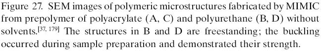
27 Neutral atomic beam lithography - neutral chromium atoms 27 B. Brezger, J. Vac. Sci. Tech. B15 (1997) 2905.
 1027.")
28 Technological trends in lithography 28 T. Ito, Nature, 406 (2000) 1027.


29 Fabrication of Nano Structure-nanomanipulation STM - xenon atoms on an single crystal nickel surface - parallel processes- field assisted diffusion sliding - perpendicular process- transfer near or on contact - field evaporation -electromigration 29 D.E. Eigler, Nature, 344 (1990) 524.

30 Fabrication of Nano Structure-nanomanipulation STM - chemical reaction 30 S.W. Hla, Phys. Rev. Lett. 85 (2000) 2775.


31 Fabrication of Nano Structure-nanomanipulation AFM - mechanical pushing 31 C. Baur, nanotechnology, 9 (1998) 360.

 T.")
13703). 32 X.")
32 Fabrication of Nano Structure-nanolithography STM - field evaporation by bias pulse on Si(111) T.T. Tsong, Phys. Rev. B44 (1991)13703). 32 X. Hu, Nanotechnology, 10 (1999) 209.


33 AFM - scratching Fabrication of Nano Structure-nanolithography Al Ti 33 A. Notargiacomo, Nanotechnology, 10 (1999) 458.


34 Fabrication of Nano Structure-nanolithography AFM - scratching the native oxide covered Si by AFM (diamond-coated tip) and electrodeposition of Cu 34 L. Santinacci, Appl. Phys. Lett. 79(2001)1882.

 M.")
35 Fabrication of Nano Structure-nanolithography AFM - nanoshaving by AFM+ surface initiated polymerization thiol initiator poly(n-isopropylacrylamide) M. Kaholek, Nanoletter, 4(2004)
36 Fabrication of Nano Structure-soft lithography Soft lithography - a set of non-photolithographic techniques for microfabrication that are based on printing of SAMs and molding of liquid precursors -reviews Y. Xia, Chem. Review, 99, 1823 (1999). Y. Xia, Angew. Chem. Int. Ed. 37, 550 (1998). Y. Xia, Annu. Rev. Mater. Sci. 28, 153 (1998). M. Geissler, Adv. Mater. 16, 1249 (2004). 36
37 Fabrication of Nano Structure-soft lithography Microcontact printing - use an elastomeric stamp with relief on its surface to generate SAMs on the surface of planar and curved substrate - SAM- highly ordered molecular assemblies that form spontaneously by chemisorption of functionalized long chain molecules on the surface of appropriate substrate ex) alkaneithiolates on Au, Ag, Cu 37
38 Fabrication of Nano Structure-soft lithography Microcontact printing - procedures 38


39 Fabrication of Nano Structure-soft lithography Microcontact printing -examples 39

40 Fabrication of Nano Structure-soft lithography Molding - micromolding in capillary 40


41 Fabrication of Nano Structure-soft lithography Molding - microtransfer molding PU on silver Epoxy on glass Glassy carbon Glass Epoxy on glass Epoxy on glass 41

42 Fabrication of Nano Structure-soft lithography Molding - replica molding gold nanostructure 42


43 Fabrication of Nano Structure-soft lithography Nanoimprint - Cr stamp PMMA above Tg Cr mask ZEP520A7 resist 43 S. Zankovych, Nanotechnology, 12 (2001) 91. I. Maximov, 13 (2002) 666.


/mica 44 R.D.")
44 Fabrication of Nano Structure-soft lithography Dip-pen lithography - direct writing based on AFM and works under ambient conditions - chemisorption acts as a driving force for moving the molecules from AFM tip to the substrate via water filled capillary when the tip is scanned across a substrate ODT on Au(111)/mica 44 R.D. Piner, Science 283 (1999) 661.

45 Fabrication of Nano Structure-soft lithography Dip-pen lithography 45 D.S. Ginger, Angew. Chem. Int. Ed. 43(2004) 30.

 Droplet during inkjet printing B)")

46 Ink Jet Printing - an attractive technique for depositing materials on surfaces with a good spatial control A Fabrication of Nano Structure-soft lithography A) Droplet during inkjet printing B) Patterning on a substrate C) Pillar formation of lead zirconium titanate B C 46 B-J de Gans, Adv. Mater. 16 (2004) 203.
")
 Patterning on a substrate C C)")

47 Fabrication of Nano Structure-soft lithography Ink Jet Printing A B A) Dependence on the viscosity of solution B) Patterning on a substrate C C) transistor fabrication (gate) using ink jet printing 47 B-J de Gans, Adv. Mater. 16 (2004) 203.
Nanostructures Fabrication Methods
 Nanostructures Fabrication Methods bottom-up methods ( atom by atom ) In the bottom-up approach, atoms, molecules and even nanoparticles themselves can be used as the building blocks for the creation of
Fabrication at the nanoscale for nanophotonics
 Fabrication at the nanoscale for nanophotonics Ilya Sychugov, KTH Materials Physics, Kista silicon nanocrystal by electron beam induced deposition lithography Outline of basic nanofabrication methods Devices
Introduction. Photoresist : Type: Structure:
 Photoresist SEM images of the morphologies of meso structures and nanopatterns on (a) a positively nanopatterned silicon mold, and (b) a negatively nanopatterned silicon mold. Introduction Photoresist
Techniken der Oberflächenphysik (Techniques of Surface Physics)
") Techniken der Oberflächenphysik (Techniques of Surface Physics) Prof. Yong Lei & Dr. Yang Xu (& Liying Liang) Fachgebiet 3D-Nanostrukturierung, Institut für Physik Contact: yong.lei@tu-ilmenau.de; yang.xu@tu-ilmenau.de;
Techniken der Oberflächenphysik (Techniques of Surface Physics) Prof. Yong Lei & Dr. Yang Xu (& Liying Liang) Fachgebiet 3D-Nanostrukturierung, Institut für Physik Contact: yong.lei@tu-ilmenau.de; yang.xu@tu-ilmenau.de;
High-density data storage: principle
 High-density data storage: principle Current approach High density 1 bit = many domains Information storage driven by domain wall shifts 1 bit = 1 magnetic nanoobject Single-domain needed Single easy axis
Fabrication of ordered array at a nanoscopic level: context
 Fabrication of ordered array at a nanoscopic level: context Top-down method Bottom-up method Classical lithography techniques Fast processes Size limitations it ti E-beam techniques Small sizes Slow processes
Nanotechnology Fabrication Methods.
 Nanotechnology Fabrication Methods. 10 / 05 / 2016 1 Summary: 1.Introduction to Nanotechnology:...3 2.Nanotechnology Fabrication Methods:...5 2.1.Top-down Methods:...7 2.2.Bottom-up Methods:...16 3.Conclusions:...19
Overview of the main nano-lithography techniques
 Overview of the main nano-lithography techniques Soraya Sangiao sangiao@unizar.es Outline Introduction: Nanotechnology. Nano-lithography techniques: Masked lithography techniques: Photolithography. X-ray
Nanotechnology Nanofabrication of Functional Materials. Marin Alexe Max Planck Institute of Microstructure Physics, Halle - Germany
 Nanotechnology Nanofabrication of Functional Materials Marin Alexe Max Planck Institute of Microstructure Physics, Halle - Germany Contents Part I History and background to nanotechnology Nanoworld Nanoelectronics
MICRO AND NANOPROCESSING TECHNOLOGIES
 LECTURE 5 MICRO AND NANOPROCESSING TECHNOLOGIES Introduction Ion lithography X-ray lithography Soft lithography E-beam lithography Concepts and processes Lithography systems Masks and resists Chapt.9.
Lecture 14 Advanced Photolithography
 Lecture 14 Advanced Photolithography Chapter 14 Wolf and Tauber 1/74 Announcements Term Paper: You are expected to produce a 4-5 page term paper on a selected topic (from a list). Term paper contributes
Nanomaterials and their Optical Applications
 Nanomaterials and their Optical Applications Winter Semester 2013 Lecture 02 rachel.grange@uni-jena.de http://www.iap.uni-jena.de/multiphoton Lecture 2: outline 2 Introduction to Nanophotonics Theoretical
Photolithography 光刻 Part II: Photoresists
 微纳光电子材料与器件工艺原理 Photolithography 光刻 Part II: Photoresists Xing Sheng 盛兴 Department of Electronic Engineering Tsinghua University xingsheng@tsinghua.edu.cn 1 Photolithography 光刻胶 负胶 正胶 4 Photolithography
UNIT 3. By: Ajay Kumar Gautam Asst. Prof. Dev Bhoomi Institute of Technology & Engineering, Dehradun
 UNIT 3 By: Ajay Kumar Gautam Asst. Prof. Dev Bhoomi Institute of Technology & Engineering, Dehradun 1 Syllabus Lithography: photolithography and pattern transfer, Optical and non optical lithography, electron,
MSN551 LITHOGRAPHY II
 MSN551 Introduction to Micro and Nano Fabrication LITHOGRAPHY II E-Beam, Focused Ion Beam and Soft Lithography Why need electron beam lithography? Smaller features are required By electronics industry:
There's Plenty of Room at the Bottom
 There's Plenty of Room at the Bottom 12/29/1959 Feynman asked why not put the entire Encyclopedia Britannica (24 volumes) on a pin head (requires atomic scale recording). He proposed to use electron microscope
Dip-Pen Lithography 1
 Dip-Pen Lithography 1 A Brief History of Writing Instruments From Quills and Bamboos to fountain pens and brushes M. Klein and Henry W. Wynne received US patent #68445 in 1867 for an ink chamber and delivery
Nano-Lithography. Edited by Stefan Landis
 Nano-Lithography Edited by Stefan Landis IST^ m WILEY Table of Contents Foreword Jörge DE SOUSA NORONHA Introduction Michel BRILLOUET xi xvii Chapter 1. X-ray Lithography: Fundamentals and Applications
Emerging nanopatterning
 Nanotechnology for engineers Winter semester 2006-2007 Emerging nanopatterning Soft-lithography: Microcontact printing Nanoimprint Lithography Stencil lithography Dip-Pen lithography / Nanoscale dispensing
Unconventional Nano-patterning. Peilin Chen
 Unconventional Nano-patterning Peilin Chen Reference Outlines History of patterning Traditional Nano-patterning Unconventional Nano-patterning Ancient Patterning "This is the Elks' land". A greeting at
Top down and bottom up fabrication
 Lecture 24 Top down and bottom up fabrication Lithography ( lithos stone / graphein to write) City of words lithograph h (Vito Acconci, 1999) 1930 s lithography press Photolithography d 2( NA) NA=numerical
Nanolithography Techniques
 Nanolithography Techniques MSE 505 / MSNT 505 P. Coane Outline What Is Nanotechnology? The Motivation For Going Small Nanofabrication Technologies Basic Techniques Nano Lithography NANOTECHNOLOGY Nanotechnology
Fabrication of micro-optical components in polymer using proton beam micro-machining and modification
 Nuclear Instruments and Methods in Physics Research B 210 (2003) 250 255 www.elsevier.com/locate/nimb Fabrication of micro-optical components in polymer using proton beam micro-machining and modification
MEEN Nanoscale Issues in Manufacturing. Lithography Lecture 1: The Lithographic Process
 MEEN 489-500 Nanoscale Issues in Manufacturing Lithography Lecture 1: The Lithographic Process 1 Discuss Reading Assignment 1 1 Introducing Nano 2 2 Size Matters 3 3 Interlude One-The Fundamental Science
Nanofabrication. with molds & stamps
 Nanofabrication with molds & stamps by Byron D. Gates A number of methods can be used to fabricate patterns with features having dimensions
Lecture 8. Photoresists and Non-optical Lithography
 Lecture 8 Photoresists and Non-optical Lithography Reading: Chapters 8 and 9 and notes derived from a HIGHLY recommended book by Chris Mack, Fundamental Principles of Optical Lithography. Any serious student
I. NANOFABRICATION O AND CHARACTERIZATION Chap. 2 : Self-Assembly
 I. Nanofabrication and Characterization : TOC I. NANOFABRICATION O AND CHARACTERIZATION Chap. 1 : Nanolithography Chap. 2 : Self-Assembly Chap. 3 : Scanning Probe Microscopy Nanoscale fabrication requirements
Technologies VII. Alternative Lithographic PROCEEDINGS OF SPIE. Douglas J. Resnick Christopher Bencher. Sponsored by. Cosponsored by.
 PROCEEDINGS OF SPIE Alternative Lithographic Technologies VII Douglas J. Resnick Christopher Bencher Editors 23-26 February 2015 San Jose, California, United States Sponsored by SPIE Cosponsored by DNS
Nano fabrication by e-beam lithographie
 Introduction to nanooptics, Summer Term 2012, Abbe School of Photonics, FSU Jena, Prof. Thomas Pertsch Nano fabrication by e-beam lithographie Lecture 14 1 Electron Beam Lithography - EBL Introduction
Optical Proximity Correction
 Optical Proximity Correction Mask Wafer *Auxiliary features added on mask 1 Overlay Errors + + alignment mask wafer + + photomask plate Alignment marks from previous masking level 2 (1) Thermal run-in/run-out
Photoresist Profile. Undercut: negative slope, common for negative resist; oxygen diffusion prohibits cross-linking; good for lift-off.
 Photoresist Profile 4-15 Undercut: negative slope, common for negative resist; oxygen diffusion prohibits cross-linking; good for lift-off undercut overcut Overcut: positive slope, common to positive resist,
Fabrication and Domain Imaging of Iron Magnetic Nanowire Arrays
 Abstract #: 983 Program # MI+NS+TuA9 Fabrication and Domain Imaging of Iron Magnetic Nanowire Arrays D. A. Tulchinsky, M. H. Kelley, J. J. McClelland, R. Gupta, R. J. Celotta National Institute of Standards
Nanostructure. Materials Growth Characterization Fabrication. More see Waser, chapter 2
 Nanostructure Materials Growth Characterization Fabrication More see Waser, chapter 2 Materials growth - deposition deposition gas solid Physical Vapor Deposition Chemical Vapor Deposition Physical Vapor
Introduction to Photolithography
 http://www.ichaus.de/news/72 Introduction to Photolithography Photolithography The following slides present an outline of the process by which integrated circuits are made, of which photolithography is
Self-assembled nanostructures for antireflection optical coatings
 Self-assembled nanostructures for antireflection optical coatings Yang Zhao 1, Guangzhao Mao 2, and Jinsong Wang 1 1. Deaprtment of Electrical and Computer Engineering 2. Departmentof Chemical Engineering
Supplementary Figure 1 Detailed illustration on the fabrication process of templatestripped
 Supplementary Figure 1 Detailed illustration on the fabrication process of templatestripped gold substrate. (a) Spin coating of hydrogen silsesquioxane (HSQ) resist onto the silicon substrate with a thickness
Three Approaches for Nanopatterning
 Three Approaches for Nanopatterning Lithography allows the design of arbitrary pattern geometry but maybe high cost and low throughput Self-Assembly offers high throughput and low cost but limited selections
Nova 600 NanoLab Dual beam Focused Ion Beam IITKanpur
 Nova 600 NanoLab Dual beam Focused Ion Beam system @ IITKanpur Dual Beam Nova 600 Nano Lab From FEI company (Dual Beam = SEM + FIB) SEM: The Electron Beam for SEM Field Emission Electron Gun Energy : 500
Presentation Phys Katia GASPERI. Statistical study of single DNA molecules into dynamic array
 Presentation Phys 730 - Katia GASPERI Statistical study of single DNA molecules into dynamic array 1 Statistical study of single DNA molecules into dynamic array - Research project lead by Laurence SALOME
Kavli Workshop for Journalists. June 13th, CNF Cleanroom Activities
 Kavli Workshop for Journalists June 13th, 2007 CNF Cleanroom Activities Seeing nm-sized Objects with an SEM Lab experience: Scanning Electron Microscopy Equipment: Zeiss Supra 55VP Scanning electron microscopes
Presentation Phys Katia GASPERI. Statistical study of single DNA molecules into dynamic array
 Presentation Phys 730 - Katia GASPERI Statistical study of single DNA molecules into dynamic array 1 Statistical study of single DNA molecules into dynamic array - Research project lead by Laurence SALOME
Nanometer scale lithography of silicon(100) surfaces using tapping mode atomic force microscopy
 surfaces using tapping mode atomic force microscopy") Nanometer scale lithography of silicon(100) surfaces using tapping mode atomic force microscopy J. Servat, a) P. Gorostiza, and F. Sanz Department Química-Fisica, Universitat de Barcelona, 08028 Barcelona,
Nanometer scale lithography of silicon(100) surfaces using tapping mode atomic force microscopy J. Servat, a) P. Gorostiza, and F. Sanz Department Química-Fisica, Universitat de Barcelona, 08028 Barcelona,
Visualization of Xe and Sn Atoms Generated from Laser-Produced Plasma for EUV Light Source
 3rd International EUVL Symposium NOVEMBER 1-4, 2004 Miyazaki, Japan Visualization of Xe and Sn Atoms Generated from Laser-Produced Plasma for EUV Light Source H. Tanaka, A. Matsumoto, K. Akinaga, A. Takahashi
Pattern Transfer- photolithography
 Pattern Transfer- photolithography DUV : EUV : 13 nm 248 (KrF), 193 (ArF), 157 (F 2 )nm H line: 400 nm I line: 365 nm G line: 436 nm Wavelength (nm) High pressure Hg arc lamp emission Ref: Campbell: 7
Nano fabrication and optical characterization of nanostructures
 Introduction to nanooptics, Summer Term 2012, Abbe School of Photonics, FSU Jena, Prof. Thomas Pertsch Nano fabrication and optical characterization of nanostructures Lecture 12 1 Optical characterization
Nanostructured Materials - Fabrication Processes 1
 FABRICATION PROCESSES FOR NANOMATERIALS - NANOSTRUCTURES Lecture 6 1 Processes 1 SUBTRACTIVE AND MODIFYING METHODS Subtractive methods: Etching: wet chemical etching, reactive ion etching; ion beam sputter
Crystalline Surfaces for Laser Metrology
 Crystalline Surfaces for Laser Metrology A.V. Latyshev, Institute of Semiconductor Physics SB RAS, Novosibirsk, Russia Abstract: The number of methodological recommendations has been pronounced to describe
Micro- and Nano-Technology... for Optics
 Micro- and Nano-Technology...... for Optics U.D. Zeitner Fraunhofer Institut für Angewandte Optik und Feinmechanik Jena Today: 1. Introduction E. Bernhard Kley Institute of Applied Physics Friedrich-Schiller
Nanosphere Lithography
 Nanosphere Lithography Derec Ciafre 1, Lingyun Miao 2, and Keita Oka 1 1 Institute of Optics / 2 ECE Dept. University of Rochester Abstract Nanosphere Lithography is quickly emerging as an efficient, low
Lithography Challenges Moore s Law Rising Costs and Challenges of Advanced Patterning
 Lithography Challenges Moore s Law Rising Costs and Challenges of Advanced Patterning SEMI Texas Spring Forum May 21, 2013 Austin, Texas Author / Company / Division / Rev. / Date A smartphone today has
Laure Fabié, Hugo Durou, Thierry Ondarçuhu Nanosciences Group, CEMES CNRS Toulouse (France)
") Nanodroplet deposition and manipulation with an AFM tip Laure Fabié, Hugo Durou, Thierry Ondarçuhu Nanosciences Group, CEMES CNRS Toulouse (France) Direct deposition methods Liquid lithography Pin and
Nanodroplet deposition and manipulation with an AFM tip Laure Fabié, Hugo Durou, Thierry Ondarçuhu Nanosciences Group, CEMES CNRS Toulouse (France) Direct deposition methods Liquid lithography Pin and
A Novel Self-aligned and Maskless Process for Formation of Highly Uniform Arrays of Nanoholes and Nanopillars
 Nanoscale Res Lett (2008) 3: 127 DOI 10.1007/s11671-008-9124-6 NANO EXPRESS A Novel Self-aligned and Maskless Process for Formation of Highly Uniform Arrays of Nanoholes and Nanopillars Wei Wu Æ Dibyendu
A. Optimizing the growth conditions of large-scale graphene films
 1 A. Optimizing the growth conditions of large-scale graphene films Figure S1. Optical microscope images of graphene films transferred on 300 nm SiO 2 /Si substrates. a, Images of the graphene films grown
DQN Positive Photoresist
 UNIVESITY OF CALIFONIA, BEKELEY BEKELEY DAVIS IVINE LOS ANGELES IVESIDE SAN DIEGO SAN FANCISCO SANTA BABAA SANTA CUZ DEPATMENT OF BIOENGINEEING 94720-1762 BioE 121 Midterm #1 Solutions BEKELEY, CALIFONIA
Nanoscale Issues in Materials & Manufacturing
 Nanoscale Issues in Materials & Manufacturing ENGR 213 Principles of Materials Engineering Module 2: Introduction to Nanoscale Issues Top-down and Bottom-up Approaches for Fabrication Winfried Teizer,
Multilayer Interference Coating, Scattering, Diffraction, Reflectivity
 Multilayer Interference Coating, Scattering, Diffraction, Reflectivity mλ = 2d sin θ (W/C, T. Nguyen) Normal incidence reflectivity 1..5 1 nm MgF 2 /Al Si C Pt, Au 1 ev 1 ev Wavelength 1 nm 1 nm.1 nm Multilayer
UNIVERSITY OF CALIFORNIA College of Engineering Department of Electrical Engineering and Computer Sciences. Professor Ali Javey. Spring 2009.
 UNIVERSITY OF CALIFORNIA College of Engineering Department of Electrical Engineering and Computer Sciences EE143 Professor Ali Javey Spring 2009 Exam 1 Name: SID: Closed book. One sheet of notes is allowed.
Lecture 3. Self-assembled Monolayers (SAM)
") 10.524 Lecture 3. Self-assembled Monolayers (SAM) Instructor: Prof. Zhiyong Gu (Chemical Engineering & UML CHN/NCOE Nanomanufacturing Center) Lecture 3: Self-assembled Monolayers (SAMs) Table of Contents
10.524 Lecture 3. Self-assembled Monolayers (SAM) Instructor: Prof. Zhiyong Gu (Chemical Engineering & UML CHN/NCOE Nanomanufacturing Center) Lecture 3: Self-assembled Monolayers (SAMs) Table of Contents
UNCONVENTIONAL NANOFABRICATION
 I 26 Mar 2004 16:10 AR AR218-MR34-11.tex AR218-MR34-11.sgm LaTeX2e(2002/01/18) P1: FHD (Some corrections may occur before final publication online and in print) R E V I E W S N A D V A N E C Annu. Rev.
SUPPLEMENTARY NOTES Supplementary Note 1: Fabrication of Scanning Thermal Microscopy Probes
 SUPPLEMENTARY NOTES Supplementary Note 1: Fabrication of Scanning Thermal Microscopy Probes Fabrication of the scanning thermal microscopy (SThM) probes is summarized in Supplementary Fig. 1 and proceeds
Deposition of Multilayer Fibers and Beads by Near-Field Electrospinning for Texturing and 3D Printing Applications
 Deposition of Multilayer Fibers and Beads by Near-Field Electrospinning for Texturing and 3D Printing Applications Nicolas Martinez-Prieto, Jian Cao, and Kornel Ehmann Northwestern University SmartManufacturingSeries.com
SOFT X-RAYS AND EXTREME ULTRAVIOLET RADIATION
 SOFT X-RAYS AND EXTREME ULTRAVIOLET RADIATION Principles and Applications DAVID ATTWOOD UNIVERSITY OF CALIFORNIA, BERKELEY AND LAWRENCE BERKELEY NATIONAL LABORATORY CAMBRIDGE UNIVERSITY PRESS Contents
Liquid nanodispensing
 Liquid nanodispensing Thierry Ondarçuhu, Laure Fabié, Erik Dujardin, Aiping Fang Nanosciences group, CEMES-CNRS, Toulouse (France) Nanopatterning, molecule deposition Dynamics of liquids at sub-micron
Au Ink for AFM Dip-Pen Nanolithography
 Letter Au Ink for AFM Dip-Pen Nanolithography Benjamin W. Maynor, Yan Li, and Jie Liu Langmuir, 2001, 17 (9), 2575-2578 DOI: 10.1021/la001755m Downloaded from http://pubs.acs.org on January 6, 2009 Subscriber
Chapter 12. Nanometrology. Oxford University Press All rights reserved.
 Chapter 12 Nanometrology Introduction Nanometrology is the science of measurement at the nanoscale level. Figure illustrates where nanoscale stands in relation to a meter and sub divisions of meter. Nanometrology
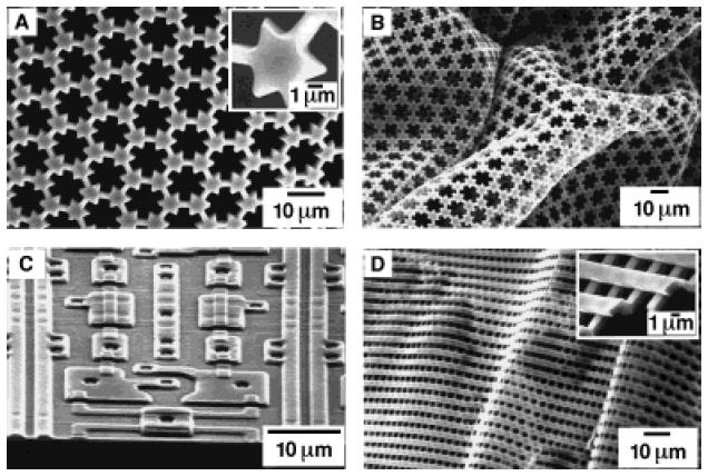
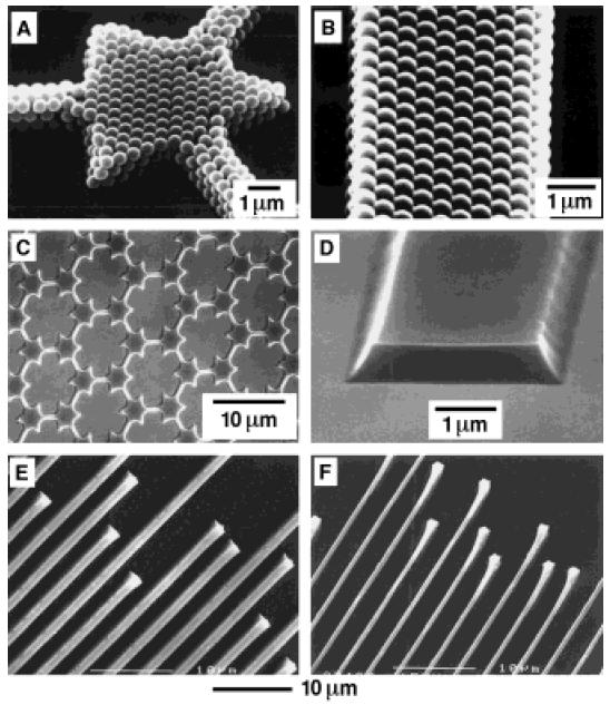
Unconventional Methods for Fabricating and Patterning Nanostructures
 Chem. Rev. 1999, 99, 1823 1848 1823 Unconventional Methods for Fabricating and Patterning Nanostructures Younan Xia, John A. Rogers, Kateri E. Paul, and George M. Whitesides*, Department of Chemistry,
Paolo Vavassori. Ikerbasque, Basque Fundation for Science and CIC nanogune Consolider, San Sebastian, Spain.
 Magnetic nanostructures Paolo Vavassori Ikerbasque, Basque Fundation for Science and CIC nanogune Consolider, San Sebastian, Spain. P. Vavassori nano@nanogune.eu I www.nanogune.eu 1 Outline Part I Introduction.
Enhanced Magnetic Properties of Bit Patterned Magnetic Recording Media by Trench-Filled Nanostructure
 CMRR Report Number 32, Summer 2009 Enhanced Magnetic Properties of Bit Patterned Magnetic Recording Media by Trench-Filled Nanostructure Edward Chulmin Choi, Daehoon Hong, Young Oh, Leon Chen, Sy-Hwang
High Accuracy EUV Reflectometry and Scattering at the Advanced Light Source
 High Accuracy EUV Reflectometry and Scattering at the Advanced Light Source Eric Gullikson Lawrence Berkeley National Laboratory 1 Reflectometry and Scattering Beamline (ALS 6.3.2) Commissioned Fall 1994
High-resolution Characterization of Organic Ultrathin Films Using Atomic Force Microscopy
 High-resolution Characterization of Organic Ultrathin Films Using Atomic Force Microscopy Jing-jiang Yu Nanotechnology Measurements Division Agilent Technologies, Inc. Atomic Force Microscopy High-Resolution
Applied Surface Science
 Applied Surface Science 254 (2008) 7064 7068 Contents lists available at ScienceDirect Applied Surface Science journal homepage: www.elsevier.com/locate/apsusc Aliphatic dithiocarboxylic acids: New adsorbates
EUV and Soft X-Ray Optics
 EUV and Soft X-Ray Optics David Attwood University of California, Berkeley Cheiron School September 2011 SPring-8 1 The short wavelength region of the electromagnetic spectrum n = 1 δ + iβ δ, β
Photolithography Overview 9/29/03 Brainerd/photoclass/ECE580/Overvie w/overview
 http://www.intel.com/research/silicon/mooreslaw.htm 1 Moore s law only holds due to photolithography advancements in reducing linewidths 2 All processing to create electric components and circuits rely
Industrial Applications of Ultrafast Lasers: From Photomask Repair to Device Physics
 Industrial Applications of Ultrafast Lasers: From Photomask Repair to Device Physics Richard Haight IBM TJ Watson Research Center PO Box 218 Yorktown Hts., NY 10598 Collaborators Al Wagner Pete Longo Daeyoung
Südliche Stadtmauerstr. 15a Tel: D Erlangen Fax:
 Curriculum Vitae Lionel Santinacci 19.10.1974 Nationality: French Südliche Stadtmauerstr. 15a Tel: + 49 9131 852 7587 D-91054 Erlangen Fax: + 49 9131 852 7582 Germany e-mail: lionel@ww.uni-erlangen.de
Plastic Electronics. Joaquim Puigdollers.
 Plastic Electronics Joaquim Puigdollers Joaquim.puigdollers@upc.edu Nobel Prize Chemistry 2000 Origins Technological Interest First products.. MONOCROMATIC PHILIPS Today Future Technological interest Low
A Photonic Crystal Laser from Solution Based. Organo-Lead Iodide Perovskite Thin Films
 SUPPORTING INFORMATION A Photonic Crystal Laser from Solution Based Organo-Lead Iodide Perovskite Thin Films Songtao Chen 1, Kwangdong Roh 2, Joonhee Lee 1, Wee Kiang Chong 3,4, Yao Lu 5, Nripan Mathews
29: Nanotechnology. What is Nanotechnology? Properties Control and Understanding. Nanomaterials
 29: Nanotechnology What is Nanotechnology? Properties Control and Understanding Nanomaterials Making nanomaterials Seeing at the nanoscale Quantum Dots Carbon Nanotubes Biology at the Nanoscale Some Applications
Chapter 10. Nanometrology. Oxford University Press All rights reserved.
 Chapter 10 Nanometrology Oxford University Press 2013. All rights reserved. 1 Introduction Nanometrology is the science of measurement at the nanoscale level. Figure illustrates where nanoscale stands
Nanoimprint Lithography
 Nanoimprint Lithography Wei Wu Quantum Science Research Advanced Studies HP Labs, Hewlett-Packard Email: wei.wu@hp.com Outline Background Nanoimprint lithography Thermal based UV-based Applications based
Figure 1: Some examples of objects at different size scales ( 2001, CMP Científica, [2])
![Figure 1: Some examples of objects at different size scales ( 2001, CMP Científica, [2])](/thumbs/85/91872790.jpg "Figure 1: Some examples of objects at different size scales ( 2001, CMP Científica, [2])") Top-Down vs. Bottom-Up Nanomanufacturing Prof. Derek J. Hansford, Biomedical Engineering Program and Department of Materials Science & Engineering Learning Objectives: This module should expose the student
Top-Down vs. Bottom-Up Nanomanufacturing Prof. Derek J. Hansford, Biomedical Engineering Program and Department of Materials Science & Engineering Learning Objectives: This module should expose the student
Nanostructured Materials and New Processing Strategies Through Polymer Chemistry
 Nanostructured Materials and New Processing Strategies Through Polymer Chemistry Professor Christopher J. Ellison McKetta Department of Chemical Engineering and Texas Materials Institute The University
Nanotechnology where size matters
 Nanotechnology where size matters J Emyr Macdonald Overview Ways of seeing very small things What is nanotechnology and why is it important? Building nanostructures What we can do with nanotechnology?
Carbon Nanotube Thin-Films & Nanoparticle Assembly
 Nanodevices using Nanomaterials : Carbon Nanotube Thin-Films & Nanoparticle Assembly Seung-Beck Lee Division of Electronics and Computer Engineering & Department of Nanotechnology, Hanyang University,
Alignment of Liquid Crystals by Ion Etched Grooved Glass Surfaces. Yea-Feng Lin, Ming-Chao Tsou, and Ru-Pin Pan
 CHINESE JOURNAL OF PHYSICS VOL. 43, NO. 6 DECEMBER 2005 Alignment of Liquid Crystals by Ion Etched Grooved Glass Surfaces Yea-Feng Lin, Ming-Chao Tsou, and Ru-Pin Pan Department of Electrophysics, National
In situ studies on dynamic properties of carbon nanotubes with metal clusters
 In situ studies on dynamic properties of carbon nanotubes with metal clusters Jason Chang, Yuan-Chih Chang, Der-Hsien Lien, Shaw-Chieh Wang*, Tung Hsu*, and Tien T. Tsong Institute of Physics, Academia
CURRENT STATUS OF NANOIMPRINT LITHOGRAPHY DEVELOPMENT IN CNMM
 U.S. -KOREA Forums on Nanotechnology 1 CURRENT STATUS OF NANOIMPRINT LITHOGRAPHY DEVELOPMENT IN CNMM February 17 th 2005 Eung-Sug Lee,Jun-Ho Jeong Korea Institute of Machinery & Materials U.S. -KOREA Forums
Nanostrukturphysik (Nanostructure Physics)
") Nanostrukturphysik (Nanostructure Physics) Prof. Yong Lei & Dr. Yang Xu Fachgebiet 3D-Nanostrukturierung, Institut für Physik Contact: yong.lei@tu-ilmenau.de; yang.xu@tu-ilmenau.de Office: Unterpoerlitzer
Nanostrukturphysik (Nanostructure Physics) Prof. Yong Lei & Dr. Yang Xu Fachgebiet 3D-Nanostrukturierung, Institut für Physik Contact: yong.lei@tu-ilmenau.de; yang.xu@tu-ilmenau.de Office: Unterpoerlitzer
UNIVERSITY OF CALIFORNIA College of Engineering Department of Electrical Engineering and Computer Sciences. Professor Ali Javey. Fall 2009.
 UNIVERSITY OF CALIFORNIA College of Engineering Department of Electrical Engineering and Computer Sciences EE143 Professor Ali Javey Fall 2009 Exam 1 Name: SID: Closed book. One sheet of notes is allowed.
Introduction to Nanotechnology Chapter 5 Carbon Nanostructures Lecture 1
 Introduction to Nanotechnology Chapter 5 Carbon Nanostructures Lecture 1 ChiiDong Chen Institute of Physics, Academia Sinica chiidong@phys.sinica.edu.tw 02 27896766 Carbon contains 6 electrons: (1s) 2,
Large-Area and Uniform Surface-Enhanced Raman. Saturation
 Supporting Information Large-Area and Uniform Surface-Enhanced Raman Spectroscopy Substrate Optimized by Enhancement Saturation Daejong Yang 1, Hyunjun Cho 2, Sukmo Koo 1, Sagar R. Vaidyanathan 2, Kelly
The fabrication of periodic metal nanodot arrays through pulsed laser melting induced fragmentation of metal nanogratings
 IOP PUBLISHING Nanotechnology 20 (2009) 285310 (5pp) NANOTECHNOLOGY doi:10.1088/0957-4484/20/28/285310 The fabrication of periodic metal nanodot arrays through pulsed laser melting induced fragmentation
Far IR Gas Lasers microns wavelengths, THz frequency Called Terahertz lasers or FIR lasers At this wavelength behaves more like
 Far IR Gas Lasers 10-1500 microns wavelengths, 300 10 THz frequency Called Terahertz lasers or FIR lasers At this wavelength behaves more like microwave signal than light Created by Molecular vibronic
Supplementary Information. Light Manipulation for Organic Optoelectronics Using Bio-inspired Moth's Eye. Nanostructures
 Supplementary Information Light Manipulation for Organic Optoelectronics Using Bio-inspired Moth's Eye Nanostructures Lei Zhou, Qing-Dong Ou, Jing-De Chen, Su Shen, Jian-Xin Tang,* Yan-Qing Li,* and Shuit-Tong
Printing Silver Nanogrids on Glass: A Hands-on Investigation of Transparent Conductive Electrodes
 Printing Silver Nanogrids on Glass: A Hands-on Investigation of Transparent Conductive Electrodes Silver Nanogrid/Nanowire Importance The next generation of optoelectronic devices requires transparent
Plasmonic Hot Hole Generation by Interband Transition in Gold-Polyaniline
 Supplementary Information Plasmonic Hot Hole Generation by Interband Transition in Gold-Polyaniline Tapan Barman, Amreen A. Hussain, Bikash Sharma, Arup R. Pal* Plasma Nanotech Lab, Physical Sciences Division,
Instrumentation and Operation
 Instrumentation and Operation 1 STM Instrumentation COMPONENTS sharp metal tip scanning system and control electronics feedback electronics (keeps tunneling current constant) image processing system data
Copyright 2001 Scientific American, Inc.
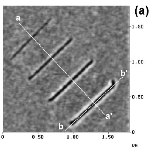
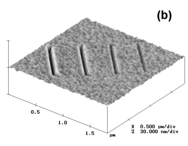
 NANOFABRICATION art The of Building Small BY GEORGE M. WHITESIDES AND J. CHRISTOPHER LOVE RESEARCHERS ARE DISCOVERING CHEAP, EFFICIENT WAYS TO MAKE STRUCTURES ONLY A FEW BILLIONTHS OF A METER ACROSS INTRICATE
Table of Contents. Foreword... Jörge DE SOUSA NORONHA. Introduction... Michel BRILLOUËT
 Table of Contents Foreword... Jörge DE SOUSA NORONHA Introduction... Michel BRILLOUËT xi xvii Chapter 1. Photolithography... 1 Philippe BANDELIER, Anne-Laure CHARLEY and Alexandre LAGRANGE 1.1. Introduction...
5. Photochemistry of polymers
 5. Photochemistry of polymers 5.1 Photopolymerization and cross-linking Photopolymerization The fundamental principle of photopolymerization is based on the photoinduced production of a reactive species,