Fabrication-II. Electron Beam Lithography Pattern Design Thin Film Deposition
|
|
|
- Marian McKinney
- 5 years ago
- Views:
Transcription
1 Fabrication-II Electron Beam Lithography Pattern Design Thin Film Deposition By Charulata Barge, Graduate student, Prof. Zumbühl Group, Department of Physics, Universtity of Basel. Date:- 20th Oct. 2006
2 Outline Scanning Electron Microscopy Electron Beam Lithography Thin film deposition Lift off process
3 Outline Scanning Electron Microscopy Electron Beam Lithography Thin film deposition lift off process
4 What is SEM? Scanning Electron Microscopy Uses electrons rather than light to form an image large depth of field produces images of high resolution
5 Principle of SEM Microscopy by employing electron beams electron beam is also referred to as "probe Electrons are used instead of optical waves smaller wavelengths can be achieved. Wavelength depends on the accelerating voltage Sample information is obtained from interaction between electrons and sample Topographical, Compositional, Elemental, Structural images can be obtained

6 Operation of SEM
7 Components of SEM The source:- Electron Gun Two emission sources:- Thermionic emitter (TE) and field emitter (FE) TE:- electrical current heats up filament FE:- filament placed in a huge electrical potential gradient The electro-magnetic lenses Electron Optical Column Vacuum system


8 The electron gun Most comman filament (Cathode):- Tungsten (W) Heated until stream of electrons is produced Accelerated by positive potential down the column -ve potential to Wehnelt cap Electrons are repelled by Wehnelt cap towards optic axix Collection of electrons:- space charge Electrons move down the column Nearly perfect point source Monochromatic source Parallel to optic axis are allowed out of gun area

9 The electro-magnetic lenses acts like an optical lens a coil of copper wires inside the iron pole pieces Circular electro-magnets - circular magnetic field in a specified region weak in the center of the gap stronger close to the bore used to focus and steer electrons
10 Electron Optical Column Two to three magnetic lenses 1) Condenser lenses :- control beam current and spot size 2)Final lens (condenser lens):- Focus the beam of electrons Deflecting coils :- move the spot forth and back stigmator coils:- correct irregularities in the beam Detectors Secondary electron detectors Back scattered electron detector
11 Vacuum system Stability of beam Ultra High vacuum and high vacuum UHV: mbar for electron optical column HV:-10-6 mbar to 10-7 mbar for chamber Rotary pump (pre-vacuum pump) Ion getter pump Turbo pump
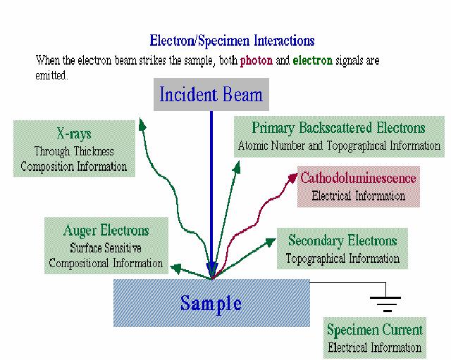
12 Specimen interactions
13 Outline Scanning Electron Microscopy Electron Beam Lithography Thin film deposition Lift off process
14 Electron Beam Lithography General Information Block diagram of EBL system Electron beam Lithography Resists Electron Scattering Factors affecting exposure
15 Lithography:- General information process used to transfer pattern from the mask/reticle to the layer of resist deposited on the surface of wafer Types of lithography photolithography (or optical lithography) uses UV radiation, X-ray lithography uses X-ray ion beam lithography uses ion beam. e-beam lithography uses electron bean
16 E-Beam Lithography E-beam lithography technique :- modified SEM system focused beam of electrons to expose the resist; Technique for creating extremely fine patterns (< 0.1μm) Process is very similar to what happens inside a television or CRT display. no mask is used as pattern is "written" directly into the resist; pattern transfer resolution below 100 nm; to manufacture high resolution masks for photolithography and X- ray lithography. Can work with a variety of resists Produces almost infinite number of patterns Slow when compared to optical lithography
17 Block Diagram on an EBL system
18 Beam Blanker for turning on / shutting off the e-beam with high precision during exposure Voltage applied to two parallel plates within beam path. Beam position moves as designated by the user.
19 Few EBL Terms Area dose= (beam current x area dwell time)/(area step size) 2 unit :- μc/cm 2 Line dose = (beam current x line dwell time)/(line step size) 2 unit :- μc/cm Dwell time :- The time the beam is still at each location. Step size : The length, the beam is moved between each dwell time, Beam current: - The e--current reaching the sample. Area dose : - The dose required for an area to fully develop that area, i.e. to remove resist. Line dose :- The dose required for a line to fully develop that line
20 Few EBL Terms Raster scan:- Vector scan Working area Write-field the electron beam is scanned across lines of pixels the wafer is shifted to the next line. an area of an individual chip is selected the beam draws out the features in that area one-by-one the part that is going to be written during exposure the area that can be covered by the e-beam with good precision For each magnification, of the design there is a certain write-field size
21 Few EBL Terms stiching If the design is larger than can be covered with one write-field, it is possible to put several write-fields adjacent to each other, with corresponding parts of the design exposed in each write-field Errors can be minimised with write field alignments The X-Y-Z stage (laser stage) high precision stage with laser-interferometric positioning system resolution 5 nm a combination of servo-motors and piezo-electric accutators
22 Pattern design The Design contains the pattern that is to be written can be made out of several "layers" Selectivity of writing The coordinates in the design called the UV coordinate system (U axis-horizontal, V-axis vertical) Alignment operations:-coordinate system is mapped on to the stage coordinate system Scaling for Area dose and line dose
23 E-Beam Resists Recording and transfer media for e-beam lithography. Polymers dissolved in a liquid solvent. Two types of e-beam resists: positive tone:- positive resists develop away exposed regions negative tone:- the developed region remains behind after development. Positive e-beam resists:-main-chain scission when exposed to e-beam Negative e-beam resists : -Formation of interchain linkages Positive e-beam resists: PMMA (Poly methyl methacrylate), EBR-9 (another acrylate based resist), PBS (Poly butene-1-sulphone), ZEP (a copolymer of a - chloromethacrylate and a -methylstyrene). Negative tone e-beam resists : COP ( an epoxy copolymer of glycidyl methacrylate and ethyl acrylate) and Shipley SAL (has 3 components, a base polymer, an acid generator, and a crosslinking agent).
24 Positive Resist Chemistry PMMA
25 Negative Resist Chemistry glycidylmethacrylate copolymers COP
26 E beam resists
27 Polymethylmethacrylate Acrylic PMMA Polymer Type:-Thermoplastic Transparent as glass and it allows 92% of the sunlight to pass Excellent clarity and UV resistance Soluble in Chlorobenzene and anisole Good abrasion resistance Hardness and stiffness. Low water absorption. Low smoke emission. Good track and arc resistance
28 PMMA thickness vs. spin speed curves
29 Electron Solid interactions Small angle forward scattering Large angle scattering events leading to backscattering. Additional exposure in the resist leading to what is called the electron beam proximity effect. Primary electrons slow down, much of their energy is dissipated in the form of secondary electrons with energies from 2 to 50 ev. Fast electrons :- secondary electrons having energy of the order of 1 kev..
30 Electron backscattering limits resolution Ref. D. Kyser and N.S. Viswanathan, J. Vac. Sc. Techn. 12, 1305(1975) Higher energy electrons have larger back-scattering range
31 Proximity Effect Collisions cause the striking electrons to 'scatter The scattering of electrons may be backward ( or back-scattering, wherein electrons 'bounce' back) scattering occurs as the electron beam interacts with the resist and substrate atoms. It broadens the diameter of the incident electron beam as it penetrates the resist and substrate It gives the resist unintended extra doses of electron exposure as back-scattered electrons from the substrate bounce back to the resist. Result in wider images Degrades the resolution of the EBL system. Closely-spaced adjacent lines can 'add' electron exposure to each other, a phenomenon known as 'proximity effect.
32 To minimize proximity effect Multilayer resist Thinner PMMA(150 nm- 200 nm) Beams of kev (can increase the backscattering) High contrast resist Proximity corrections of dose and spot size Low beam energies:- electron range is smaller than the minimum feature size
33 Developing the resist Chemicals used:- For PMMA 1:3 MIBK:IPA +1.3% MEK MIBK:- Methyl Isobutyl Ketone IPA:- Isopropyl alcohol MEK:- methyl ethyl ketone MEK gives better contrast The exposed part is removed Surface is cleaned with Isopropyl alcohol
34 Outline Scanning Electron Microscopy Electron Beam Lithography Thin film deposition Lift off process
35 Thin Film Deposition Depositing a thin film of material onto a substrate Types of deposition techniques Chemical deposition Plating Chemical vapor deposition (CVD) Plasma enhanced CVD Physical deposition Resistance thermal evaporator Electron beam evaporator Sputtering Pulsed laser deposition Other methods Reactive sputtering Molecular beam epitaxy Topotaxy,
 by heating a large current is passed through a filament")

36 Resistance Thermal evaporation Commonly used metal deposition technique. "indirect" thermal evaporation Vaporizing a solid material (pure metal, eutectic or compound) by heating a large current is passed through a filament container (usually in the shape of a basket, boat or crucible) which has a finite electrical resistance. The choice of this filament material is dictated by the evaporation temperature and its inertness to alloying/chemical reaction with the evaporant. Pressures lower than 1e-5 mbar are necessary Substrate-to-source distance of approximately 10 to 50 cm in a vacuum chamber. Good vacuum is a prerequisite
 A current (5 to 10 kv) is sent through a tungsten filament Thermionic emission of electrons takes")

37 Electron Beam Evaporation Under vacuum, typically 10E-5 or deeper. (rotary and turbo pumps) A current (5 to 10 kv) is sent through a tungsten filament Thermionic emission of electrons takes place. The filament is located in an area outside the deposition zone, in order to avoid contamination. The electrons are focused and directed toward the evaporant The kinetic energy of ebeam motion is transformed to heat High energy is released often more than several million watts per square inch
38 Comparision Method Pro Con Metals and compunds E-Beam Evaporation 1. high temp materials 2. good for liftoff 1. alloys difficult 2. poor step coverage Al, Ti, Au, Ni, Ge, Cr, Cu, Pd, and Pt 3. highest purity Thermal Evaporation 1. simple to implement 2. good for liftoff 1. limited source material (no high temp) 2. alloys difficult 3. poor step coverage Al,Au,AuGe,In, Ni,Ti,Zn, SiO
39 Outline Scanning Electron Microscopy Electron Beam Lithography Thin film deposition Lift off process
40 Lift Off Process What is lift off? Ideal lift off process General procedure and Chemicals used for lift off
41 What is lift off? Process allowing definition of pattern on the wafer surface without etching To define geometry for metals which are hard to etch metals such as gold; Metal is lifted off in selected areas by dissolving underlying resist. Typically used for GaAs.

42 Ideal lift off process Substrate Spin Resist Pattern and develop resist Metal deposition Positive resist Remove resist Negative resist

43 PMMA undercut and metal deposition Substrate Spin Resist Pattern and develop resist Metal deposition PMMA Remove resist
44 General procedure and chemicals Chemicals used :- Acetone and Isopropanol Procedure:- Immerse sample in warm (50 0 C) acetone for min. Avoid contamination of the metal and resist on sample (use syring) Immerse sample in IPA for 5 min. Blow dry
:- 60 nm Wafer:-Si Resist:- PMMA Spin speed:- 6000 rpm D( PMMA):- 430nm Evaporant :-gold D(gold):-")
45 Dose test samples Wafer:- Si Resist:- PMMA Spin speed: rpm D( PMMA):- 500nm Evaporant :- gold D(gold):- 60 nm Wafer:-Si Resist:- PMMA Spin speed: rpm D( PMMA):- 430nm Evaporant :-gold D(gold):- 60 nm
46 Thank you for your attention
Introduction to Electron Beam Lithography
 Introduction to Electron Beam Lithography Boštjan Berčič (bostjan.bercic@ijs.si), Jožef Štefan Institute, Jamova 39, 1000 Ljubljana, Slovenia 1. Introduction Electron Beam Lithography is a specialized
Supplementary Figure 1 Detailed illustration on the fabrication process of templatestripped
 Supplementary Figure 1 Detailed illustration on the fabrication process of templatestripped gold substrate. (a) Spin coating of hydrogen silsesquioxane (HSQ) resist onto the silicon substrate with a thickness
Photoresist Profile. Undercut: negative slope, common for negative resist; oxygen diffusion prohibits cross-linking; good for lift-off.
 Photoresist Profile 4-15 Undercut: negative slope, common for negative resist; oxygen diffusion prohibits cross-linking; good for lift-off undercut overcut Overcut: positive slope, common to positive resist,
Nano fabrication by e-beam lithographie
 Introduction to nanooptics, Summer Term 2012, Abbe School of Photonics, FSU Jena, Prof. Thomas Pertsch Nano fabrication by e-beam lithographie Lecture 14 1 Electron Beam Lithography - EBL Introduction
Scanning Electron Microscopy
 Scanning Electron Microscopy Field emitting tip Grid 2kV 100kV Anode ZEISS SUPRA Variable Pressure FESEM Dr Heath Bagshaw CMA bagshawh@tcd.ie Why use an SEM? Fig 1. Examples of features resolvable using
UNIT 3. By: Ajay Kumar Gautam Asst. Prof. Dev Bhoomi Institute of Technology & Engineering, Dehradun
 UNIT 3 By: Ajay Kumar Gautam Asst. Prof. Dev Bhoomi Institute of Technology & Engineering, Dehradun 1 Syllabus Lithography: photolithography and pattern transfer, Optical and non optical lithography, electron,
MSN551 LITHOGRAPHY II
 MSN551 Introduction to Micro and Nano Fabrication LITHOGRAPHY II E-Beam, Focused Ion Beam and Soft Lithography Why need electron beam lithography? Smaller features are required By electronics industry:
Gaetano L Episcopo. Scanning Electron Microscopy Focus Ion Beam and. Pulsed Plasma Deposition
 Gaetano L Episcopo Scanning Electron Microscopy Focus Ion Beam and Pulsed Plasma Deposition Hystorical background Scientific discoveries 1897: J. Thomson discovers the electron. 1924: L. de Broglie propose
Nova 600 NanoLab Dual beam Focused Ion Beam IITKanpur
 Nova 600 NanoLab Dual beam Focused Ion Beam system @ IITKanpur Dual Beam Nova 600 Nano Lab From FEI company (Dual Beam = SEM + FIB) SEM: The Electron Beam for SEM Field Emission Electron Gun Energy : 500
Metal Deposition. Filament Evaporation E-beam Evaporation Sputter Deposition
 Metal Deposition Filament Evaporation E-beam Evaporation Sputter Deposition 1 Filament evaporation metals are raised to their melting point by resistive heating under vacuum metal pellets are placed on
6.5 Optical-Coating-Deposition Technologies
 92 Chapter 6 6.5 Optical-Coating-Deposition Technologies The coating process takes place in an evaporation chamber with a fully controlled system for the specified requirements. Typical systems are depicted
Technology for Micro- and Nanostructures Micro- and Nanotechnology
 Lecture 5: Electron-Beam Lithography, Part 1 Technology for Micro- and Nanostructures Micro- and Nanotechnology Peter Unger mailto: peter.unger @ uni-ulm.de Institute of Optoelectronics University of Ulm
DEPOSITION OF THIN TiO 2 FILMS BY DC MAGNETRON SPUTTERING METHOD
 Chapter 4 DEPOSITION OF THIN TiO 2 FILMS BY DC MAGNETRON SPUTTERING METHOD 4.1 INTRODUCTION Sputter deposition process is another old technique being used in modern semiconductor industries. Sputtering
Supplementary Information Effects of asymmetric nanostructures on the extinction. difference properties of actin biomolecules and filaments
 Supplementary Information Effects of asymmetric nanostructures on the extinction difference properties of actin biomolecules and filaments 1 E. H. Khoo, 2 Eunice S. P. Leong, 1 W. K. Phua, 2 S. J. Wu,
Lecture 14 Advanced Photolithography
 Lecture 14 Advanced Photolithography Chapter 14 Wolf and Tauber 1/74 Announcements Term Paper: You are expected to produce a 4-5 page term paper on a selected topic (from a list). Term paper contributes
Photolithography 光刻 Part II: Photoresists
 微纳光电子材料与器件工艺原理 Photolithography 光刻 Part II: Photoresists Xing Sheng 盛兴 Department of Electronic Engineering Tsinghua University xingsheng@tsinghua.edu.cn 1 Photolithography 光刻胶 负胶 正胶 4 Photolithography
object objective lens eyepiece lens
 Advancing Physics G495 June 2015 SET #1 ANSWERS Field and Particle Pictures Seeing with electrons The compound optical microscope Q1. Before attempting this question it may be helpful to review ray diagram
= 6 (1/ nm) So what is probability of finding electron tunneled into a barrier 3 ev high?
 So what is probability of finding electron tunneled into a barrier 3 ev high?") STM STM With a scanning tunneling microscope, images of surfaces with atomic resolution can be readily obtained. An STM uses quantum tunneling of electrons to map the density of electrons on the surface
STM STM With a scanning tunneling microscope, images of surfaces with atomic resolution can be readily obtained. An STM uses quantum tunneling of electrons to map the density of electrons on the surface
Auger Electron Spectroscopy (AES) Prof. Paul K. Chu
 Prof. Paul K. Chu") Auger Electron Spectroscopy (AES) Prof. Paul K. Chu Auger Electron Spectroscopy Introduction Principles Instrumentation Qualitative analysis Quantitative analysis Depth profiling Mapping Examples The Auger
Auger Electron Spectroscopy (AES) Prof. Paul K. Chu Auger Electron Spectroscopy Introduction Principles Instrumentation Qualitative analysis Quantitative analysis Depth profiling Mapping Examples The Auger
Kavli Workshop for Journalists. June 13th, CNF Cleanroom Activities
 Kavli Workshop for Journalists June 13th, 2007 CNF Cleanroom Activities Seeing nm-sized Objects with an SEM Lab experience: Scanning Electron Microscopy Equipment: Zeiss Supra 55VP Scanning electron microscopes
Presentation Phys Katia GASPERI. Statistical study of single DNA molecules into dynamic array
 Presentation Phys 730 - Katia GASPERI Statistical study of single DNA molecules into dynamic array 1 Statistical study of single DNA molecules into dynamic array - Research project lead by Laurence SALOME
TMT4320 Nanomaterials November 10 th, Thin films by physical/chemical methods (From chapter 24 and 25)
") 1 TMT4320 Nanomaterials November 10 th, 2015 Thin films by physical/chemical methods (From chapter 24 and 25) 2 Thin films by physical/chemical methods Vapor-phase growth (compared to liquid-phase growth)
1 TMT4320 Nanomaterials November 10 th, 2015 Thin films by physical/chemical methods (From chapter 24 and 25) 2 Thin films by physical/chemical methods Vapor-phase growth (compared to liquid-phase growth)
Electron Microprobe Analysis 1 Nilanjan Chatterjee, Ph.D. Principal Research Scientist
 12.141 Electron Microprobe Analysis 1 Nilanjan Chatterjee, Ph.D. Principal Research Scientist Massachusetts Institute of Technology Electron Microprobe Facility Department of Earth, Atmospheric and Planetary
Electron Microprobe Analysis 1 Nilanjan Chatterjee, Ph.D. Principal Research Scientist
 12.141 Electron Microprobe Analysis 1 Nilanjan Chatterjee, Ph.D. Principal Research Scientist Massachusetts Institute of Technology Electron Microprobe Facility Department of Earth, Atmospheric and Planetary
AP5301/ Name the major parts of an optical microscope and state their functions.
 Review Problems on Optical Microscopy AP5301/8301-2015 1. Name the major parts of an optical microscope and state their functions. 2. Compare the focal lengths of two glass converging lenses, one with
SUPPORTING INFORMATION: Titanium Contacts to Graphene: Process-Induced Variability in Electronic and Thermal Transport
 SUPPORTING INFORMATION: Titanium Contacts to Graphene: Process-Induced Variability in Electronic and Thermal Transport Keren M. Freedy 1, Ashutosh Giri 2, Brian M. Foley 2, Matthew R. Barone 1, Patrick
MICROCHIP MANUFACTURING by S. Wolf
 by S. Wolf Chapter 15 ALUMINUM THIN-FILMS and SPUTTER-DEPOSITION 2004 by LATTICE PRESS CHAPTER 15 - CONTENTS Aluminum Thin-Films Sputter-Deposition Process Steps Physics of Sputter-Deposition Magnetron-Sputtering
MICRO AND NANOPROCESSING TECHNOLOGIES
 LECTURE 5 MICRO AND NANOPROCESSING TECHNOLOGIES Introduction Ion lithography X-ray lithography Soft lithography E-beam lithography Concepts and processes Lithography systems Masks and resists Chapt.9.
Electron beam scanning
 Electron beam scanning The Electron beam scanning operates through an electro-optical system which has the task of deflecting the beam Synchronously with cathode ray tube which create the image, beam moves
Nanostructure. Materials Growth Characterization Fabrication. More see Waser, chapter 2
 Nanostructure Materials Growth Characterization Fabrication More see Waser, chapter 2 Materials growth - deposition deposition gas solid Physical Vapor Deposition Chemical Vapor Deposition Physical Vapor
Part II: Thin Film Characterization
 Part II: Thin Film Characterization General details of thin film characterization instruments 1. Introduction to Thin Film Characterization Techniques 2. Structural characterization: SEM, TEM, AFM, STM
Supporting Information. Metallic Adhesion Layer Induced Plasmon Damping and Molecular Linker as a Non-Damping Alternative
 Supporting Information Metallic Adhesion Layer Induced Plasmon Damping and Molecular Linker as a Non-Damping Alternative Terefe G. Habteyes, Scott Dhuey, Erin Wood, Daniel Gargas, Stefano Cabrini, P. James
Presentation Phys Katia GASPERI. Statistical study of single DNA molecules into dynamic array
 Presentation Phys 730 - Katia GASPERI Statistical study of single DNA molecules into dynamic array 1 Statistical study of single DNA molecules into dynamic array - Research project lead by Laurence SALOME
A Photonic Crystal Laser from Solution Based. Organo-Lead Iodide Perovskite Thin Films
 SUPPORTING INFORMATION A Photonic Crystal Laser from Solution Based Organo-Lead Iodide Perovskite Thin Films Songtao Chen 1, Kwangdong Roh 2, Joonhee Lee 1, Wee Kiang Chong 3,4, Yao Lu 5, Nripan Mathews
Enhanced Transmission by Periodic Hole. Arrays in Metal Films
 Enhanced Transmission by Periodic Hole Arrays in Metal Films K. Milliman University of Florida July 30, 2008 Abstract Three different square periodic hole arrays were manufactured on a silver film in order
Magnon-drag thermopile
 Magnon-drag thermopile I. DEVICE FABRICATION AND CHARACTERIZATION Our devices consist of a large number of pairs of permalloy (NiFe) wires (30 nm wide, 20 nm thick and 5 µm long) connected in a zigzag
Introduction to Photolithography
 http://www.ichaus.de/news/72 Introduction to Photolithography Photolithography The following slides present an outline of the process by which integrated circuits are made, of which photolithography is
Secondary ion mass spectrometry (SIMS)
") Secondary ion mass spectrometry (SIMS) ELEC-L3211 Postgraduate Course in Micro and Nanosciences Department of Micro and Nanosciences Personal motivation and experience on SIMS Offers the possibility to
Secondary ion mass spectrometry (SIMS) ELEC-L3211 Postgraduate Course in Micro and Nanosciences Department of Micro and Nanosciences Personal motivation and experience on SIMS Offers the possibility to
Supplementary Information Our InGaN/GaN multiple quantum wells (MQWs) based one-dimensional (1D) grating structures
 based one-dimensional (1D) grating structures") Polarized white light from hybrid organic/iii-nitrides grating structures M. Athanasiou, R. M. Smith, S. Ghataora and T. Wang* Department of Electronic and Electrical Engineering, University of Sheffield,
Polarized white light from hybrid organic/iii-nitrides grating structures M. Athanasiou, R. M. Smith, S. Ghataora and T. Wang* Department of Electronic and Electrical Engineering, University of Sheffield,
STRONG DOUBLE LAYER STRUCTURE IN THERMIONIC VACUUM ARC PLASMA *
 STRONG DOUBLE LAYER STRUCTURE IN THERMIONIC VACUUM ARC PLASMA * V. TIRON 1, L. MIHAESCU 1, C.P. LUNGU 2 and G. POPA 1 1 Faculty of Physics, Al. I. Cuza University, 700506, Iasi, Romania 2 National Institute
Repetition: Practical Aspects
 Repetition: Practical Aspects Reduction of the Cathode Dark Space! E x 0 Geometric limit of the extension of a sputter plant. Lowest distance between target and substrate V Cathode (Target/Source) - +
Optical Proximity Correction
 Optical Proximity Correction Mask Wafer *Auxiliary features added on mask 1 Overlay Errors + + alignment mask wafer + + photomask plate Alignment marks from previous masking level 2 (1) Thermal run-in/run-out
Auger Electron Spectroscopy
 Auger Electron Spectroscopy Auger Electron Spectroscopy is an analytical technique that provides compositional information on the top few monolayers of material. Detect all elements above He Detection
Infrastructure of Thin Films Laboratory in Institute of Molecular Physics Polish Academy of Sciences
 Infrastructure of Thin Films Laboratory in Institute of Molecular Physics Polish Academy of Sciences Outline Sample preparation Magnetron sputtering Ion-beam sputtering Pulsed laser deposition Electron-beam
J. Photopolym. Sci. Technol., Vol. 22, No. 5, Fig. 1. Orthogonal solvents to conventional process media.
 originates from the limited number of options regarding orthogonal solvents, i.e. solvents that do not dissolve or adversely damage a pre-deposited organic materials layer. The simplest strategy to achieve
Basic structure of SEM
 Table of contents Basis structure of SEM SEM imaging modes Comparison of ordinary SEM and FESEM Electron behavior Electron matter interaction o Elastic interaction o Inelastic interaction o Interaction
Toward Clean Suspended CVD Graphene
 Electronic Supplementary Material (ESI) for RSC Advances. This journal is The Royal Society of Chemistry 2016 Supplemental information for Toward Clean Suspended CVD Graphene Alexander Yulaev 1,2,3, Guangjun
Chapter 9. Electron mean free path Microscopy principles of SEM, TEM, LEEM
 Chapter 9 Electron mean free path Microscopy principles of SEM, TEM, LEEM 9.1 Electron Mean Free Path 9. Scanning Electron Microscopy (SEM) -SEM design; Secondary electron imaging; Backscattered electron
Why microscopy?
 Electron Microscopy Why microscopy? http://www.cellsalive.com/howbig.htm 2 Microscopes are used as magnifying tools (although not exclusively as will see later on). The resolution of the human eye is limited
MSE 321 Structural Characterization
 Auger Spectroscopy Auger Electron Spectroscopy (AES) Scanning Auger Microscopy (SAM) Incident Electron Ejected Electron Auger Electron Initial State Intermediate State Final State Physical Electronics
Nanostructures Fabrication Methods
 Nanostructures Fabrication Methods bottom-up methods ( atom by atom ) In the bottom-up approach, atoms, molecules and even nanoparticles themselves can be used as the building blocks for the creation of
LECTURE 5 SUMMARY OF KEY IDEAS
 LECTURE 5 SUMMARY OF KEY IDEAS Etching is a processing step following lithography: it transfers a circuit image from the photoresist to materials form which devices are made or to hard masking or sacrificial
Fabrication at the nanoscale for nanophotonics
 Fabrication at the nanoscale for nanophotonics Ilya Sychugov, KTH Materials Physics, Kista silicon nanocrystal by electron beam induced deposition lithography Outline of basic nanofabrication methods Devices
Introduction to X-ray Photoelectron Spectroscopy (XPS) XPS which makes use of the photoelectric effect, was developed in the mid-1960
 XPS which makes use of the photoelectric effect, was developed in the mid-1960") Introduction to X-ray Photoelectron Spectroscopy (XPS) X-ray Photoelectron Spectroscopy (XPS), also known as Electron Spectroscopy for Chemical Analysis (ESCA) is a widely used technique to investigate
Introduction to X-ray Photoelectron Spectroscopy (XPS) X-ray Photoelectron Spectroscopy (XPS), also known as Electron Spectroscopy for Chemical Analysis (ESCA) is a widely used technique to investigate
Modern Optical Spectroscopy
 Modern Optical Spectroscopy X-Ray Microanalysis Shu-Ping Lin, Ph.D. Institute of Biomedical Engineering E-mail: splin@dragon.nchu.edu.tw Website: http://web.nchu.edu.tw/pweb/users/splin/ Backscattered
Supporting Information
 Supporting Information Assembly and Densification of Nanowire Arrays via Shrinkage Jaehoon Bang, Jonghyun Choi, Fan Xia, Sun Sang Kwon, Ali Ashraf, Won Il Park, and SungWoo Nam*,, Department of Mechanical
Supporting Information
 Copyright WILEY-VCH Verlag GmbH & Co. KGaA, 69469 Weinheim, Germany, 2017. Supporting Information for Adv. Mater., DOI: 10.1002/adma.201702682 Dynamics of Templated Assembly of Nanoparticle Filaments within
Pattern Transfer- photolithography
 Pattern Transfer- photolithography DUV : EUV : 13 nm 248 (KrF), 193 (ArF), 157 (F 2 )nm H line: 400 nm I line: 365 nm G line: 436 nm Wavelength (nm) High pressure Hg arc lamp emission Ref: Campbell: 7
ABC s of Electrochemistry series Materials Characterization techniques: SEM and EDS Ana María Valenzuela-Muñiz November 3, 2011
 ABC s of Electrochemistry series Materials Characterization techniques: SEM and EDS Ana María Valenzuela-Muñiz November 3, 2011 CEER, Department of Chemical and Biomolecular Engineering Outline Introduction
Applications of Electron Beam Lithography (EBL) in Optoelectronics Device Fabrication
 in Optoelectronics Device Fabrication") AASCIT Journal of Physics 2018; 4(2): 53-58 http://www.aascit.org/journal/physics ISSN: 2381-1358 (Print); ISSN: 2381-1366 (Online) Applications of Electron Beam Lithography (EBL) in Optoelectronics Device
AASCIT Journal of Physics 2018; 4(2): 53-58 http://www.aascit.org/journal/physics ISSN: 2381-1358 (Print); ISSN: 2381-1366 (Online) Applications of Electron Beam Lithography (EBL) in Optoelectronics Device
SUPPLEMENTARY MATERIALS FOR PHONON TRANSMISSION COEFFICIENTS AT SOLID INTERFACES
 148 A p p e n d i x D SUPPLEMENTARY MATERIALS FOR PHONON TRANSMISSION COEFFICIENTS AT SOLID INTERFACES D.1 Overview The supplementary information contains additional information on our computational approach
tip conducting surface
 PhysicsAndMathsTutor.com 1 1. The diagram shows the tip of a scanning tunnelling microscope (STM) above a conducting surface. The tip is at a potential of 1.0 V relative to the surface. If the tip is sufficiently
E-Beam Nanolithography Integrated with Scanning Electron Microscope
 5 E-Beam Nanolithography Integrated with Scanning Electron Microscope Joe Nabity, Lesely Anglin Campbell, Mo Zhu, and Weilie Zhou 1. Introduction 1.1. Basics of Microscope-Based Lithography Electron beams
Overview of the main nano-lithography techniques
 Overview of the main nano-lithography techniques Soraya Sangiao sangiao@unizar.es Outline Introduction: Nanotechnology. Nano-lithography techniques: Masked lithography techniques: Photolithography. X-ray
ORION NanoFab: An Overview of Applications. White Paper
 ORION NanoFab: An Overview of Applications White Paper ORION NanoFab: An Overview of Applications Author: Dr. Bipin Singh Carl Zeiss NTS, LLC, USA Date: September 2012 Introduction With the advancement
X-Ray Photoelectron Spectroscopy (XPS) Prof. Paul K. Chu
 Prof. Paul K. Chu") X-Ray Photoelectron Spectroscopy (XPS) Prof. Paul K. Chu X-ray Photoelectron Spectroscopy Introduction Qualitative analysis Quantitative analysis Charging compensation Small area analysis and XPS imaging
X-Ray Photoelectron Spectroscopy (XPS) Prof. Paul K. Chu X-ray Photoelectron Spectroscopy Introduction Qualitative analysis Quantitative analysis Charging compensation Small area analysis and XPS imaging
Supporting Information s for
 Supporting Information s for # Self-assembling of DNA-templated Au Nanoparticles into Nanowires and their enhanced SERS and Catalytic Applications Subrata Kundu* and M. Jayachandran Electrochemical Materials
A Novel Approach to the Layer Number-Controlled and Grain Size- Controlled Growth of High Quality Graphene for Nanoelectronics
 Supporting Information A Novel Approach to the Layer Number-Controlled and Grain Size- Controlled Growth of High Quality Graphene for Nanoelectronics Tej B. Limbu 1,2, Jean C. Hernández 3, Frank Mendoza
Techniken der Oberflächenphysik (Techniques of Surface Physics)
") Techniken der Oberflächenphysik (Techniques of Surface Physics) Prof. Yong Lei & Dr. Yang Xu (& Liying Liang) Fachgebiet 3D-Nanostrukturierung, Institut für Physik Contact: yong.lei@tu-ilmenau.de; yang.xu@tu-ilmenau.de;
Techniken der Oberflächenphysik (Techniques of Surface Physics) Prof. Yong Lei & Dr. Yang Xu (& Liying Liang) Fachgebiet 3D-Nanostrukturierung, Institut für Physik Contact: yong.lei@tu-ilmenau.de; yang.xu@tu-ilmenau.de;
SEM Optics and Application to Current Research
 SEM Optics and Application to Current Research Azure Avery May 28, 2008 1 Introduction 1.1 History The optical microscope was invented in the early 17th century. Although revolutionary, the earliest microscopes
XPS/UPS and EFM. Brent Gila. XPS/UPS Ryan Davies EFM Andy Gerger
 XPS/UPS and EFM Brent Gila XPS/UPS Ryan Davies EFM Andy Gerger XPS/ESCA X-ray photoelectron spectroscopy (XPS) also called Electron Spectroscopy for Chemical Analysis (ESCA) is a chemical surface analysis
Vacuum Pumps. Two general classes exist: Gas transfer physical removal of matter. Mechanical, diffusion, turbomolecular
 Vacuum Technology Vacuum Pumps Two general classes exist: Gas transfer physical removal of matter Mechanical, diffusion, turbomolecular Adsorption entrapment of matter Cryo, sublimation, ion Mechanical
Electrochemical Deposition of Iron Nanoparticles on PPY and H terminated Si substrates. Karan Sukhija Co-op Term # 1 April 28 th, 2005
 Electrochemical Deposition of Iron Nanoparticles on PPY and H terminated Si substrates Karan Sukhija Co-op Term # 1 April 28 th, 2005 Future Suggested Experiments Acknowledgments Presentation Outline Background
Fundamentals of Electron Beam Exposure
 Fundamentals of Electron Beam Exposure 2 and Development Mohammad Ali Mohammad, Mustafa Muhammad, Steven K. Dew, and Maria Stepanova Abstract Electron Beam Lithography (EBL) is a fundamental technique
Low Voltage Field Emission SEM (LV FE-SEM): A Promising Imaging Approach for Graphene Samples
: A Promising Imaging Approach for Graphene Samples") Low Voltage Field Emission SEM (LV FE-SEM): A Promising Imaging Approach for Graphene Samples Jining Xie Agilent Technologies May 23 rd, 2012 www.agilent.com/find/nano Outline 1. Introduction 2. Agilent
Low Voltage Field Emission SEM (LV FE-SEM): A Promising Imaging Approach for Graphene Samples Jining Xie Agilent Technologies May 23 rd, 2012 www.agilent.com/find/nano Outline 1. Introduction 2. Agilent
Introduction to Thin Film Processing
 Introduction to Thin Film Processing Deposition Methods Many diverse techniques available Typically based on three different methods for providing a flux of atomic or molecular material Evaporation Sputtering
Nanosphere Lithography
 Nanosphere Lithography Derec Ciafre 1, Lingyun Miao 2, and Keita Oka 1 1 Institute of Optics / 2 ECE Dept. University of Rochester Abstract Nanosphere Lithography is quickly emerging as an efficient, low
Case Study of Electronic Materials Packaging with Poor Metal Adhesion and the Process for Performing Root Cause Failure Analysis
 Case Study of Electronic Materials Packaging with Poor Metal Adhesion and the Process for Performing Root Cause Failure Analysis Dr. E. A. Leone BACKGRUND ne trend in the electronic packaging industry
Nanoimprint Lithography
 Nanoimprint Lithography Wei Wu Quantum Science Research Advanced Studies HP Labs, Hewlett-Packard Email: wei.wu@hp.com Outline Background Nanoimprint lithography Thermal based UV-based Applications based
Fabrication and Domain Imaging of Iron Magnetic Nanowire Arrays
 Abstract #: 983 Program # MI+NS+TuA9 Fabrication and Domain Imaging of Iron Magnetic Nanowire Arrays D. A. Tulchinsky, M. H. Kelley, J. J. McClelland, R. Gupta, R. J. Celotta National Institute of Standards
Stepwise Solution Important Instructions to examiners:
 (ISO/IEC - 700-005 Certified) SUMMER 05 EXAMINATION Subject Code: 70 Model Answer (Applied Science- Physics) Page No: 0/6 Que. No. Sub. Que. Important Instructions to examiners: ) The answers should be
Introduction. Photoresist : Type: Structure:
 Photoresist SEM images of the morphologies of meso structures and nanopatterns on (a) a positively nanopatterned silicon mold, and (b) a negatively nanopatterned silicon mold. Introduction Photoresist
Figure 1: Graphene release, transfer and stacking processes. The graphene stacking began with CVD
 Supplementary figure 1 Graphene Growth and Transfer Graphene PMMA FeCl 3 DI water Copper foil CVD growth Back side etch PMMA coating Copper etch in 0.25M FeCl 3 DI water rinse 1 st transfer DI water 1:10
Clean-Room microfabrication techniques. Francesco Rizzi Italian Institute of Technology
 Clean-Room microfabrication techniques Francesco Rizzi Italian Institute of Technology Miniaturization The first transistor Miniaturization The first transistor Miniaturization The first transistor Miniaturization
Auger Electron Spectroscopy (AES)
") 1. Introduction Auger Electron Spectroscopy (AES) Silvia Natividad, Gabriel Gonzalez and Arena Holguin Auger Electron Spectroscopy (Auger spectroscopy or AES) was developed in the late 1960's, deriving
1. Introduction Auger Electron Spectroscopy (AES) Silvia Natividad, Gabriel Gonzalez and Arena Holguin Auger Electron Spectroscopy (Auger spectroscopy or AES) was developed in the late 1960's, deriving
EE C245 ME C218 Introduction to MEMS Design Fall 2007
 EE C245 ME C218 Introduction to MEMS Design Fall 2007 Prof. Clark T.-C. Nguyen Dept. of Electrical Engineering & Computer Sciences University of California at Berkeley Berkeley, CA 94720 Lecture 5: ALD,
Formation and Surface Modification of Nanopatterned Thiol-ene Substrates using
 Supporting Information Formation and Surface Modification of Nanopatterned Thiol-ene Substrates using Step and Flash Imprint Lithography Vaibhav S. Khire, 1 Youngwoo Yi, 2 Noel A. Clark, 2 and Christopher
Chapter 3 : ULSI Manufacturing Technology - (c) Photolithography
 Photolithography") Chapter 3 : ULSI Manufacturing Technology - (c) Photolithography 1 Reference 1. Semiconductor Manufacturing Technology : Michael Quirk and Julian Serda (2001) 2. - (2004) 3. Semiconductor Physics and Devices-
Chapter 3 : ULSI Manufacturing Technology - (c) Photolithography 1 Reference 1. Semiconductor Manufacturing Technology : Michael Quirk and Julian Serda (2001) 2. - (2004) 3. Semiconductor Physics and Devices-
HOW TO APPROACH SCANNING ELECTRON MICROSCOPY AND ENERGY DISPERSIVE SPECTROSCOPY ANALYSIS. SCSAM Short Course Amir Avishai
 HOW TO APPROACH SCANNING ELECTRON MICROSCOPY AND ENERGY DISPERSIVE SPECTROSCOPY ANALYSIS SCSAM Short Course Amir Avishai RESEARCH QUESTIONS Sea Shell Cast Iron EDS+SE Fe Cr C Objective Ability to ask the
Everhart-Thornley detector
 SEI Detector Everhart-Thornley detector Microscope chamber wall Faraday cage Scintillator Electrons in Light pipe Photomultiplier Electrical signal out Screen Quartz window +200 V +10 kv Always contains
ZEP520 ZEP520. Technical Report. ZEON CORPORATION Specialty Materials Division. High Resolution Positive Electron Beam Resist.
 Technical Report ZEP52 ZEP52 Ver.1.2 Mar.21 ZEONREX Electronic Chemicals High Resolution Positive Electron Beam Resist ZEP52 ZEON CORPORATION Specialty Materials Division Headquarters R&D Center Furukawa
Supporting Information
 Electronic Supplementary Material (ESI) for ChemComm. This journal is The Royal Society of Chemistry 2014 Supporting Information Controllable Atmospheric Pressure Growth of Mono-layer, Bi-layer and Tri-layer
Questions on Electric Fields
 Questions on Electric Fields 1. The diagram shows a positively charged oil drop held at rest between two parallel conducting plates A and B. Oil drop A B 2.50 cm The oil drop has a mass 9.79 x 10 15 kg.
MSE 321 Structural Characterization
 Auger Spectroscopy Auger Electron Spectroscopy (AES) Scanning Auger Microscopy (SAM) Incident Electron Ejected Electron Auger Electron Initial State Intermediate State Final State Physical Electronics
Two-Dimensional (C 4 H 9 NH 3 ) 2 PbBr 4 Perovskite Crystals for. High-Performance Photodetector. Supporting Information for
 2 PbBr 4 Perovskite Crystals for. High-Performance Photodetector. Supporting Information for") Supporting Information for Two-Dimensional (C 4 H 9 NH 3 ) 2 PbBr 4 Perovskite Crystals for High-Performance Photodetector Zhenjun Tan,,ǁ, Yue Wu,ǁ, Hao Hong, Jianbo Yin, Jincan Zhang,, Li Lin, Mingzhan
Supporting Information for Two-Dimensional (C 4 H 9 NH 3 ) 2 PbBr 4 Perovskite Crystals for High-Performance Photodetector Zhenjun Tan,,ǁ, Yue Wu,ǁ, Hao Hong, Jianbo Yin, Jincan Zhang,, Li Lin, Mingzhan
ETCHING Chapter 10. Mask. Photoresist
 ETCHING Chapter 10 Mask Light Deposited Substrate Photoresist Etch mask deposition Photoresist application Exposure Development Etching Resist removal Etching of thin films and sometimes the silicon substrate
PHI 5000 Versaprobe-II Focus X-ray Photo-electron Spectroscopy
 PHI 5000 Versaprobe-II Focus X-ray Photo-electron Spectroscopy The very basic theory of XPS XPS theroy Surface Analysis Ultra High Vacuum (UHV) XPS Theory XPS = X-ray Photo-electron Spectroscopy X-ray
ELEMENT2 High Resolution- ICP-MS INSTRUMENT OVERVIEW
 ELEMENT2 High Resolution- ICP-MS INSTRUMENT OVERVIEW Inductively Coupled Plasma Mass Spectrometry (ICP-MS) What is a Plasma? - The magnetic field created by a RF (radio frequency) coil produces
Lecture 22 Ion Beam Techniques
 Lecture 22 Ion Beam Techniques Schroder: Chapter 11.3 1/44 Announcements Homework 6/6: Will be online on later today. Due Wednesday June 6th at 10:00am. I will return it at the final exam (14 th June).
Ultrafast X-Ray-Matter Interaction and Damage of Inorganic Solids October 10, 2008
 Ultrafast X-Ray-Matter Interaction and Damage of Inorganic Solids October 10, 2008 Richard London rlondon@llnl.gov Workshop on Interaction of Free Electron Laser Radiation with Matter Hamburg This work