Why microscopy?
|
|
|
- Nigel Gaines
- 6 years ago
- Views:
Transcription
1 Electron Microscopy

2 Why microscopy? 2 Microscopes are used as magnifying tools (although not exclusively as will see later on). The resolution of the human eye is limited and can only distinguish points separated by about 100 microns. Anything below this requires some sort of magnification.


3 Why microscopy? Detail resolved Unresolved A common misconception in microscopy is that more magnification is always better. Very often people ask how much does the instrument magnify? This is not the correct question, which should be how little can it resolve?. An empty magnification occurs when the magnification exceeds the limits imposed by resolution, i.e., no additional information is provided by the optical system in spite of the high magnification. 3

4 Resolution of an optical system Rayleigh criterion If two image points are far away from each other, they are easily recognized as separate objects. However, when the distance between them is reduced, a limit point is reached whenthemaximumofthefirstairydiskcoincideswiththefirstminimumofthesecondairy disk. The superimposed profiles display two brightness maxima that are separated by a valley. The intensity in the valley is reduced by approximately 20 percent compared with the two maxima. Thisisjustsufficientforthehumaneyeto seetwo separate points, a limitthat 4 is referred to as the Rayleigh criterion.

 is given by: ρ = 1.22λ/ 2 (n.sinµ)( = 0.")
5 Resolution of an optical system Diffraction at an aperture - Rayleigh criterion The Rayleigh criterion for the resolution of an optical system states that two points can be resolved if the maximum of the intensity of the Airy ring from one of them coincides with the first minimum intensity of the Airy ring of the other. This implies that the resolution, ρ (strictly speaking, the resolving power) is given by: ρ = 1.22λ/ 2 (n.sinµ)( = 0.61λ/NA where λ is the wavelength, n the refractive index and µ is the semi-angle at the specimen. NA is the numerical aperture: minimum resolvable detail ρ should be small! 1 point 2 points 2 points resolved 5 unresolved
6 Electron Microscopy
7
8 Comparison between Optical and Electron Microscopy: In many ways, electron microscopes (Scanning and Transmission) are analogous to light microscopes. Fundamentally and functionally, electron microscopes (EM) and optical microscopes (OM) are identical. That is, both types of microscopes serve to magnify objects normally invisible to the naked eyes. Basically, component terminology of an EM is similar to that of an OM. Both microscopes consist on the following:
9 (a) Source of Illumination as light source Electron Gun produces an electron beam by thermionic or field emission - EM Lamp produces light beam (including uv rays) - OM (b) Condenser Lens system projects a near parallel radiation on to the specimen Electro-magnets of variable focal length are the lenses in EM. Curved transparent substance - OM (c) Series of Imaging Lenses form the Image of the specimen
10
11 TABLE 1. EM and OM Comparison Chart PARAMETERS OPTICAL MICROSCOPE ELECTRON MICROSCOPE Illuminating Beam Light Beam Electron Beam 7,500Å (visible) 0.859Å (20 kv) Wavelength ~2,000Å (ultraviolet) ~0.0370Å (100 kv) Medium Atmosphere Vacuum Lens Optical lens (glass) Electron Lens (magnetic or electrostatic) Resolving Power Visible: 3,000Å Ultraviolet: 1,000Å Point to point: 3Å Lattice: 1.4Å Aperture Angle 70 o ~35 10x ~ 2,000x 90x ~ 800,000x Magnification (lens exchange) (continuously variable) Focusing Mechanically Electrically Contrast Absorption, Reflection Scattering absorption -SEM Diffraction, phase - TEM Sample Type Bulk sample Bulk sample - SEM Thin foil ( 3 mm dia. and electron transparent, i.e atoms in thickness) -TEM Information Grain size and shape Distribution of phases (particles) Grain size and shape Distribution of phases (particles) Chemical composition, e.g Identify phases Crystal and defect structure
12 Principles of Electron Microscopy
13 Scanning Electron Microscopy (SEM) Scanning electron microscopy is used to observe topographies of specimens at very high magnifications. SEM magnifications can go to more than 500,000 X but most applications require magnifications of less than 50,000 X. During SEM inspection, a beam of electrons is focused on a spot volume of the specimen. These bombarding electrons, also referred to as primary electrons, removing electrons from the specimen itself. The outgoing electrons, also known as secondary electrons, are attracted and collected by a positively biased grid or detector. To produce the SEM image, the electron beam is swept across the area being inspected. The signals are then amplified, analyzed, and translated into images of the topography being inspected. Finally, the image is shown on a CRT monitor.


14 SEM - Working principles An electron gun generates electrons. A condenser lens focus the beam to form the smallest point possible. There are then scanning coils that deflect the beam and make it raster the sample surface. When the beam hits the sample, it generates several signal types (the electrons are accelerated by kv and have therefore a high kinetic energy). If a detector is used to detect one of those signal types we can attribute to each point a signal intensity. Therefore, if we feed a CRT monitor with the signal in a synchronized way with can build 14 an image point by point.
15
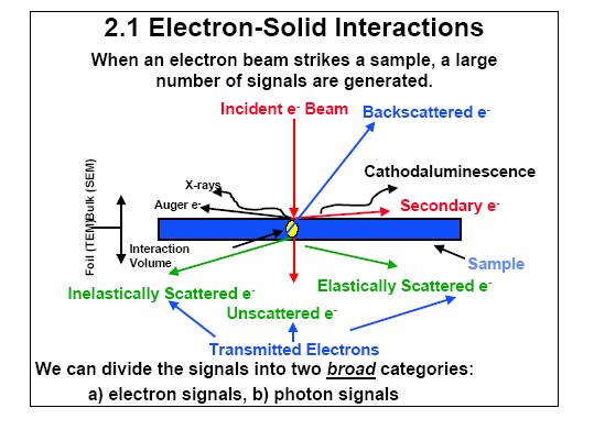
16 Figure 1. Summary of the various signals obtained by interaction of electrons with matter in an electron microscope
17 ~ 50 nm SEM Beam/specimen interactions
18 Scanning Electron Microscopy (SEM) The energy of the primary electrons determines the quantity of secondary electrons collected during inspection. The emission of secondary electrons from the specimen increases as the energy of the primary electron beam increases, until a certain limit is reached. Beyond this limit, the collected secondary electrons diminish as the energy of the primary beam is increased, because the primary beam is already activating electrons deep below the surface of the specimen. Electrons coming from such depths usually recombine before reaching the surface for emission. Aside from secondary electrons, the primary electron beam results in the emission of backscattered (or reflected) electrons from the specimen. Backscattered electrons possess more energy than secondary electrons, and have a definite direction. As such, they can not be collected by a secondary electron detector, unless the detector is directly in their path of travel. All emissions above 50 ev are considered to be backscattered electrons.
19 ELECTRON SOURCES Electron sources in electron beam instruments are required to provide either a large total current beam of about 50 µm diameter - low magnification and TEM, or a high intensity probe of electrons as small as 0.5 nm in diameter - SEM There are three different types of electron source available


20 Electron gun cathodes Tungsten Hairpin Filament LaB 6 Pointed Rod FEG Tungsten field-emission cathode 20 (FEG = Field Emission Gun)
21 There are three different types of electron source available a) Thermionic tungsten hairpin filament This is usually heated to about 2800 K by direct resistance heating. The surrounding grid, known as the Wehnelt cylinder and the anode, which is at earth potential, act as an electrostatic lens. For an operating condition of 100 kv, the brightness is about 3 x 10 5 A cm -2.
22 b) Lanthanium hexaboride crystal (LaB 6 ) The only difference between the conventional assembly and a modern LaB 6 assembly is that extra pumping holes are present in the Wehnelt cap to ensure a better pumping speed near the tip. Higher current (greater than the tungsten) is obtainable in small probes. The brightness of a LaB 6 can be as high as 10 7 A cm -2 at 100kV (3 x 10 5 A cm -2, in thermionic filaments).
23 c) Field emission source This is usually a <111> orientation crystal of tungsten, and a Wehnelt cylinder, which is raised to an extraction potential up to about 4 kv in order to cause emission from the tip of the crystal. There is a requirement of high vacuum for this source. The brightness of cold or thermal emission source can be about 10 4 times of a conventional tungsten filament. The high brightness of this source make them preferable for scanning instruments.


24 Electron gun field emission In the field emission gun, a very strong electric field (10 9 Vm -1 ) is used to extract electrons from a metal filament. Temperatures are lower than that needed for thermionic emission. This gives a higher source brightness that in thermionic guns, but requires a very good vacuum. In order to get high field strengths with low voltages, the field emitting tip has a strong curvature. The emitting region can be less than 10 nm. The grid provides the field which extracts the electrons by a tunneling mechanism. The combination of a modest potential with a very small tip radius results in a very high field strength. The anode is a positively charged metal plate (i.e., at earth potential), that has a hole in it. Its function it to accelerate the electron beam towards the specimen. 24

25 Electron gun cathodes Electron Gun - Thermionic vs Field Emission 25
26 ELECTRON LENSES AND OPTICS

27 Electromagnetic lenses The electron microscopes have electromagnetic lenses which are basically coils that generate an electromagnetic field that acts on the electrons, focusing them as glass lenses focuses light. One of the practical differences between the optical microscope and the electron microscopes is that these have dynamic lenses like our eyes that can adapt as opposed to glass lens that have fixed characteristics. That is, if one wants to increase magnification in an optical microscope, it is necessary to change the objective, whereas in the electron microscope you just have to turn a knob and supply more current to the lens to make it stronger. 27
28 Scanning Electro-magnets steer the beam so it scans the sample. sample


29 SEM - Signal detection SE = secondary electrons BSE = Backscatter electrons EDS = X-Ray Energy Dispersive Spectroscopy VP = variable pressure (environmental SEM) 29

30 SEM Electron signal types Energy distribution of SE and BSE Plasmon losses 30 (primary beam energy)
 secondary electrons.")
31 SEM - Everhart-Thornley electron detector (SE) The detector consists primarily of a scintillator inside a Faraday cage. A low positive voltage is applied to the Faraday cage to attract the relatively low energy (less than 50 ev) secondary electrons. Other electrons within the specimen chamber are not attracted by this low voltage and will only reach the detector if their direction of travel takes them to it. The scintillator has a high positive voltage (~10 kv) to accelerate the incoming electrons to it where they can be converted to light photons. The direction of their travel is focused to the light guide by a metal coating on the scintillator acting as a mirror. In the light pipe the photons travel outside of the 31microscope's vacuum chamber to a photomultiplier tube for amplification.
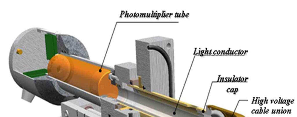
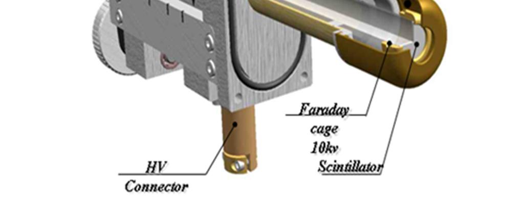
32 32 SEM - Everhart-Thornley electron detector (SE)
33
34 Typical Information from Electron Microscope: Imaging (surface) can be characterized using secondary electrons, backscattered electrons, photoelectrons, Auger electrons and ion scattering. Crystallography or crystal structure information can be obtained from backscattered electrons (diffraction of photons or electrons). Chemical composition of materials can be obtained using electron microprobes to produce characteristic X-ray emissions and electron energy losses. The various studies of materials exploit at least one of the above information, as well as the excellent spatial resolution of electron microscopes.


 35")
35 SEM - Topographic contrast (SE) (where do the shades come from?) 35 Rippel E.M. Facility
, but can only escape if they are originating from near the surface.")
36 SEM - Topographic contrast (SE) (where do the shades come from?) The images obtained with the SE signal look as if they had topographic contrast, how is this contrast formed? SE are generated throughout the whole interaction volume (IV), but can only escape if they are originating from near the surface. In a hill there is more exposed surface of the IV: more SE escape and signal is higher. In the valleys there is less surface exposed and less SE escape. Hills appear as bright regions and valleys as dark regions in SE images.


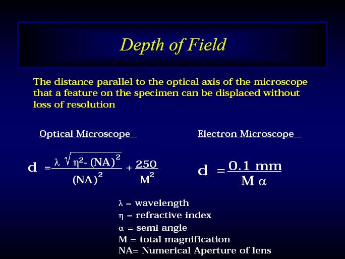
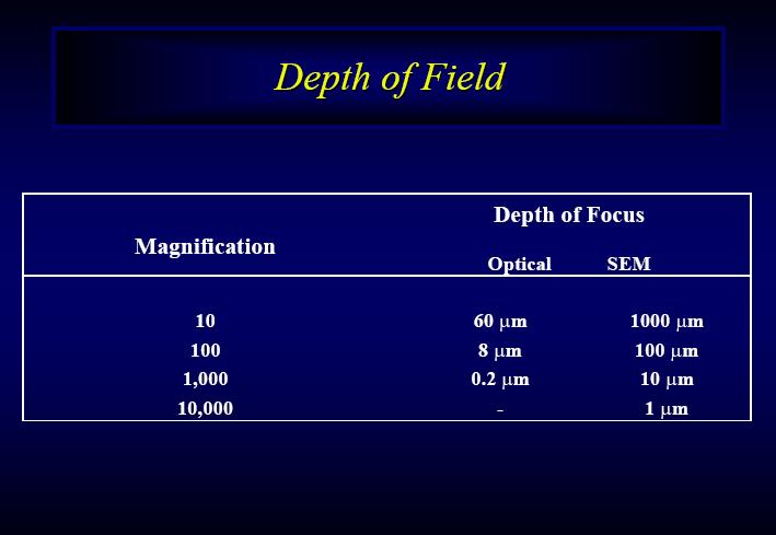
37 SEM - Depth of field (SE) Optical vs SEM Optical Microscope Image SEM Image of Same Object The SEM has a great advantage its high depth of field. You can see in this image an object imaged with an OM and while you see some point in focus, the ones just below or just above are defocused. This does happen with the SEM image, where you see the whole object in focus. 37
38
39
40 Resolution: Resolution defines the smallest separation of two points in the object, which may be distinctly reproduced in the image. The resolving power for light microscopy is determined by diffraction aberration and can be defined as ρ = k λ nsin α where λ is the wavelength of the illumination, n is the refractive index of the medium between the specimen and the lens, α is the semi-angle (aperture angle) subtended by the object at the lens and k is a constant usually taken to be 0.61.
41 Light vs electrons The wavelengths of electrons are much smaller and by using the Rayleigh criterion we can see that an optical microscope can resolve ~ 2000 Angstroms, while the electron microscope can resolve ~ angstroms ρ = 0.61 λ / (n sinα) Nowadays TEMs can resolve in the sub-angstrom range 41
42 Variation of Electron Wavelength with applied voltage A p p lie d V o lta g e (k e V ) W a v e le n g th, λ (n m ) The ultimate resolution of an electron microscope is dictated not by wavelength but by the defects in the imaging system (diffraction aberration) of the radiation employed.
, as this would induce perturbation of the primary beam.")
43 SEM - Backscattered electron detector BSE are primary electrons bounced by the sample that are not easily collected due to their high energy: their trajectory cannot be changed with an external potential (as with the SE detector), as this would induce perturbation of the primary beam. To maximize collection the detector is concentric and below the objective lens 43


44 BSE Detector Primary e-beam Obj. lens BSE Detector - M - e Conductive sample Residual gas molecule High vacuum


45 SEM - SE vs BSE electron images Topographic contrast (SE mode) Atomic number contrast (BSE mode) BSE are used because their emission is sensitive to the atomic number, contrarily to the SE signal. The same region observed with the two signal types. The bright regions in the SE image correspond to hills, whereas the bright regions in the BSE image correspond to the presence of heavier elements. Heavier elements scatter electron more efficiently so show up brighter in the images. This atomic number contrast is a major advantage of the BSE detector. 45
46 SEM Compositional contrast (BSE) BSE images 46
47 Scanning Electron Microscopy (SEM) Backscattered electron imaging is useful in distinguishing one material from another, since the yield of the collected backscattered electrons increases monotonically with the specimen's atomic number. Backscatter imaging can distinguish elements with atomic number differences of at least 3, i.e., materials with atomic number differences of at least 3 would appear with good contrast on the image. A SEM may also be equipped with na EDX analysis system to perform compositional analysis on specimens. EDX analysis is useful in identifying materials and contaminants, as well as estimating their relative concentrations on the surface of the specimen.
48


49 Sample preparation Samples need to be electrically conductive. Samples are analyzed under vacuum and biological samples need careful and complex preparation. How to turn a mosquito conductive?
50 50 SEM - Biological Sample Preparation Biological structures collapse under vacuum Fixation/dehydration/drying/mounting/coating Fixation: Stabilization of biological material. Chemical fixation (cross-linking) with Aldehydes or OsO 4. Dehydration: Substitution of water with solvent (ethanol, acetone) Usually performed with gradient of different concentrations. Critical point drying: replace ethanol with CO 2 brought to critical point (31.1 C and 1,073 psi), becomes dense vapor phase; Gaseous CO 2 vented slowly to avoid condensation. Or Hexametildisilizane (HMDS) drying: transition from ethanol to HMDS (reduces capillarity effects during drying), left overnight in desiccator with silica gel. Mounting: on a stub that can be inserted in the SEM sample holder. Coating: with conductive layer: Prevent charging effects that hinder suitable image formation.


51 Typical SEM images Coloured image of soybean cyst nematode and egg. The colour makes it easier for nonspecialists to understand the structures. SEM image of normal circulating human blood. SEM image of an electronic component. 51 All except one image have a problem. Why? No scale bar...
52 Environmental SEM Environmental secondary electrons detector The environmental Secondary Detector uses gas ionization to amplify the secondary electron signal. In nonconductive samples, positive ions are attracted to the sample surface where negative charges from the beam tend to accumulate. The positive ions effectively suppress charge artifacts!!! What are the implications for ceramic, polymer and biological samples observation? 52

53 Environmental SEM Environmental secondary electrons detector What are the implications for ceramic, polymer and biological samples observation? The negative charge accumulated in non-conductive samples is balanced by the positive ions: no-coating needed. 53
54 Environmental SEM Known compromises: Gas-electron interations radially scatter the primary electrons away from de intended landing point. Function of: gas type, pressure, path length acceleration voltage Primary beam current cannot be directly measured and it fluctuates with pressure (EDS X-ray maps are diffuse and point analysis require normalization Useful for biological samples as they can be observed without vacuum (even living). Useful for non conductive samples as the positive ions anhilate charge effects. No conducting coating is required but resolution is lower then with standard SEMs. Most instruments can also operate at high vaccum and have a standard SE detector 54
55 Crystallography : Crystal structure analysis is usually based on diffraction phenomena caused by the interaction of matter with X-rays, electrons, or neutrons. Therefore, when either X-rays or electrons interact with crystalline material, they are: (a) Subject to diffraction have similar wave properties. (b) Monochromatic radiation - produce a series of strongly diffracted beams leaving the crystal in defined and predicted directions.
56 The resultant diffraction pattern is given by Bragg s Law, and this is given by n λ = 2d sinθ where, Note d: Interplanar spacing θ: Grazing angle of incidence (Bragg angle) n: Integer (0, 1, 2, 3.. ) λ: Wavelength of the incident electrons With diffraction, we use Reciprocal lattice in which sets of lattice planes are represented simply by a set of points in reciprocal space.
57 Table 1. Characteristics of Light and Radiations Used for Diffraction. Light Neutrons X-rays Electrons Wavelength [nm] Energy [ev] E E E+05 Charge [C] E-19 Rest mass [g] E E-28 Penetration depth [mm] E-03 Electrons are the only radiation in which their penetration depth and interaction volume is small enough to allow diffraction from individual grains (very small volume). Hence, only electrons can be used for MICROTEXTURE
58 CHEMICAL COMPOSITION Energy dispersive X-ray spectroscopy (EDS) Wavelength dispersive X-ray spectroscopy (WDS) 58
59 Advantages vs Disadvantages of Advantages SEM - high depth of field - direct observation of the external form of real objects at high magnifications - wide range of magnifications (below 50 x to over x) - local chemical and crystallographic analyzes Disadvantages of SEM - high vacuum environment of the specimen (difficult with porous materials, damaging for biological samples ) - inability to show internal detail - inability to obtain highest resolution - conductive samples: The samples need to be conductive because otherwise they tend to charge and eventually charging pertubates the primary beam and signal detection. 59
= 6 (1/ nm) So what is probability of finding electron tunneled into a barrier 3 ev high?
 So what is probability of finding electron tunneled into a barrier 3 ev high?") STM STM With a scanning tunneling microscope, images of surfaces with atomic resolution can be readily obtained. An STM uses quantum tunneling of electrons to map the density of electrons on the surface
STM STM With a scanning tunneling microscope, images of surfaces with atomic resolution can be readily obtained. An STM uses quantum tunneling of electrons to map the density of electrons on the surface
Scanning Electron Microscopy
 Scanning Electron Microscopy Field emitting tip Grid 2kV 100kV Anode ZEISS SUPRA Variable Pressure FESEM Dr Heath Bagshaw CMA bagshawh@tcd.ie Why use an SEM? Fig 1. Examples of features resolvable using
AP5301/ Name the major parts of an optical microscope and state their functions.
 Review Problems on Optical Microscopy AP5301/8301-2015 1. Name the major parts of an optical microscope and state their functions. 2. Compare the focal lengths of two glass converging lenses, one with
Electron Microprobe Analysis 1 Nilanjan Chatterjee, Ph.D. Principal Research Scientist
 12.141 Electron Microprobe Analysis 1 Nilanjan Chatterjee, Ph.D. Principal Research Scientist Massachusetts Institute of Technology Electron Microprobe Facility Department of Earth, Atmospheric and Planetary
Electron Microprobe Analysis 1 Nilanjan Chatterjee, Ph.D. Principal Research Scientist
 12.141 Electron Microprobe Analysis 1 Nilanjan Chatterjee, Ph.D. Principal Research Scientist Massachusetts Institute of Technology Electron Microprobe Facility Department of Earth, Atmospheric and Planetary
Part II: Thin Film Characterization
 Part II: Thin Film Characterization General details of thin film characterization instruments 1. Introduction to Thin Film Characterization Techniques 2. Structural characterization: SEM, TEM, AFM, STM
Basic structure of SEM
 Table of contents Basis structure of SEM SEM imaging modes Comparison of ordinary SEM and FESEM Electron behavior Electron matter interaction o Elastic interaction o Inelastic interaction o Interaction
object objective lens eyepiece lens
 Advancing Physics G495 June 2015 SET #1 ANSWERS Field and Particle Pictures Seeing with electrons The compound optical microscope Q1. Before attempting this question it may be helpful to review ray diagram
Analytical Methods for Materials
 Analytical Methods for Materials Lesson 21 Electron Microscopy and X-ray Spectroscopy Suggested Reading Leng, Chapter 3, pp. 83-126; Chapter 4, pp. 127-160; Chapter 6, pp. 191-219 P.J. Goodhew, J. Humphreys
Modern Optical Spectroscopy
 Modern Optical Spectroscopy X-Ray Microanalysis Shu-Ping Lin, Ph.D. Institute of Biomedical Engineering E-mail: splin@dragon.nchu.edu.tw Website: http://web.nchu.edu.tw/pweb/users/splin/ Backscattered
MSE 321 Structural Characterization
 Optical Microscope Plan Lenses In an "ideal" single-element lens system all planar wave fronts are focused to a point at distance f from the lens; therefore: Image near the optical axis will be in perfect
Transmission Electron Microscopy
 L. Reimer H. Kohl Transmission Electron Microscopy Physics of Image Formation Fifth Edition el Springer Contents 1 Introduction... 1 1.1 Transmission Electron Microscopy... 1 1.1.1 Conventional Transmission
Electron Microprobe Analysis and Scanning Electron Microscopy
 Electron Microprobe Analysis and Scanning Electron Microscopy Electron microprobe analysis (EMPA) Analytical technique in which a beam of electrons is focused on a sample surface, producing X-rays from
Weak-Beam Dark-Field Technique
 Basic Idea recall bright-field contrast of dislocations: specimen close to Bragg condition, s î 0 Weak-Beam Dark-Field Technique near the dislocation core, some planes curved to s = 0 ) strong Bragg reflection
Chapter 9. Electron mean free path Microscopy principles of SEM, TEM, LEEM
 Chapter 9 Electron mean free path Microscopy principles of SEM, TEM, LEEM 9.1 Electron Mean Free Path 9. Scanning Electron Microscopy (SEM) -SEM design; Secondary electron imaging; Backscattered electron
Electron beam scanning
 Electron beam scanning The Electron beam scanning operates through an electro-optical system which has the task of deflecting the beam Synchronously with cathode ray tube which create the image, beam moves
Gaetano L Episcopo. Scanning Electron Microscopy Focus Ion Beam and. Pulsed Plasma Deposition
 Gaetano L Episcopo Scanning Electron Microscopy Focus Ion Beam and Pulsed Plasma Deposition Hystorical background Scientific discoveries 1897: J. Thomson discovers the electron. 1924: L. de Broglie propose
M2 TP. Low-Energy Electron Diffraction (LEED)
") M2 TP Low-Energy Electron Diffraction (LEED) Guide for report preparation I. Introduction: Elastic scattering or diffraction of electrons is the standard technique in surface science for obtaining structural
M2 TP Low-Energy Electron Diffraction (LEED) Guide for report preparation I. Introduction: Elastic scattering or diffraction of electrons is the standard technique in surface science for obtaining structural
The illumination source: the electron beam
 The SEM Column The illumination source: the electron beam The probe of the electron microscope is an electron beam with very high and stable energy (10-100 kev) in order to get images with high resolution.
Practical course in scanning electron microscopy
 Practical course in scanning electron microscopy Fortgeschrittenen Praktikum an der Technischen Universität München Wintersemester 2017/2018 Table of contents 1. Introduction 3 2. Formation of an electron
h p λ = mν Back to de Broglie and the electron as a wave you will learn more about this Equation in CHEM* 2060
 Back to de Broglie and the electron as a wave λ = mν h = h p you will learn more about this Equation in CHEM* 2060 We will soon see that the energies (speed for now if you like) of the electrons in the
Scanning Electron Microscopy & Ancillary Techniques
 Scanning Electron Microscopy & Ancillary Techniques By Pablo G. Caceres-Valencia The prototype of the first Stereoscan supplied by the Cambridge Instrument Company to the dupont Company, U.S.A. (1965)
Invited Lecture. "Different Aspects of Electron Microscopy. Sardar Vallabhbhai National Institute of Technology, Surat. Deepak Rajput & S.K.
 Invited Lecture on "Different Aspects of Electron Microscopy at Sardar Vallabhbhai National Institute of Technology, Surat Deepak Rajput & S.K. Tiwary R&D and Product Development Essar Steel Limited Abstract
Ecole Franco-Roumaine : Magnétisme des systèmes nanoscopiques et structures hybrides - Brasov, Modern Analytical Microscopic Tools
 1. Introduction Solid Surfaces Analysis Group, Institute of Physics, Chemnitz University of Technology, Germany 2. Limitations of Conventional Optical Microscopy 3. Electron Microscopies Transmission Electron
tip conducting surface
 PhysicsAndMathsTutor.com 1 1. The diagram shows the tip of a scanning tunnelling microscope (STM) above a conducting surface. The tip is at a potential of 1.0 V relative to the surface. If the tip is sufficiently
Nano-Microscopy. Lecture 2. Scanning and Transmission Electron Microscopies: Principles. Pavel Zinin HIGP, University of Hawaii, Honolulu, USA
 GG 711: Advanced Techniques in Geophysics and Materials Science Nano-Microscopy. Lecture 2 Scanning and Transmission Electron Microscopies: Principles Pavel Zinin HIGP, University of Hawaii, Honolulu,
Part I Basics and Methods
 j1 Part I Basics and Methods In-situ Electron Microscopy: Applications in Physics, Chemistry and Materials Science, First Edition. Edited by Gerhard Dehm, James M. Howe, and Josef Zweck. Ó 2012 Wiley-VCH
Introduction to Electron Microscopy Andres Kaech. Instrumentation
 Center for Microscopy and Image Analysis Introduction to Electron Microscopy Andres Kaech Instrumentation The types of electron microscopes Transmission electron microscope (TEM) Scanning electron microscope
Everhart-Thornley detector
 SEI Detector Everhart-Thornley detector Microscope chamber wall Faraday cage Scintillator Electrons in Light pipe Photomultiplier Electrical signal out Screen Quartz window +200 V +10 kv Always contains
SEM Optics and Application to Current Research
 SEM Optics and Application to Current Research Azure Avery May 28, 2008 1 Introduction 1.1 History The optical microscope was invented in the early 17th century. Although revolutionary, the earliest microscopes
High-Resolution. Transmission. Electron Microscopy
 Part 4 High-Resolution Transmission Electron Microscopy 186 Significance high-resolution transmission electron microscopy (HRTEM): resolve object details smaller than 1nm (10 9 m) image the interior of
INDIAN INSTITUTE OF TECHNOLOGY ROORKEE NPTEL NPTEL ONLINE CERTIFICATION COURSE. Biomedical Nanotechnology. Lec-05 Characterisation of Nanoparticles
 INDIAN INSTITUTE OF TECHNOLOGY ROORKEE NPTEL NPTEL ONLINE CERTIFICATION COURSE Biomedical Nanotechnology Lec-05 Characterisation of Nanoparticles Dr. P. Gopinath Department of Biotechnology Indian Institute
Scanning Electron Microscopy
 Scanning Electron Microscopy Amanpreet Kaur 1 www.reading.ac.uk/emlab Scanning Electron Microscopy What is scanning electron microscopy? Basic features of conventional SEM Limitations of conventional SEM
SEM stands for Scanning Electron Microscopy. The earliest known work describing
 1. HISTORY ABOUT SEM SEM stands for Scanning Electron Microscopy. The earliest known work describing the concept of a Scanning Electron Microscope was by M. Knoll (1935) who, along with other pioneers
MT Electron microscopy Scanning electron microscopy and electron probe microanalysis
 MT-0.6026 Electron microscopy Scanning electron microscopy and electron probe microanalysis Eero Haimi Research Manager Outline 1. Introduction Basics of scanning electron microscopy (SEM) and electron
ABC s of Electrochemistry series Materials Characterization techniques: SEM and EDS Ana María Valenzuela-Muñiz November 3, 2011
 ABC s of Electrochemistry series Materials Characterization techniques: SEM and EDS Ana María Valenzuela-Muñiz November 3, 2011 CEER, Department of Chemical and Biomolecular Engineering Outline Introduction
sin" =1.22 # D "l =1.22 f# D I: In introduction to molecular electron microscopy - Imaging macromolecular assemblies
 I: In introduction to molecular electron microscopy - Imaging macromolecular assemblies Yifan Cheng Department of Biochemistry & Biophysics office: GH-S472D; email: ycheng@ucsf.edu 2/20/2015 - Introduction
PHI 5000 Versaprobe-II Focus X-ray Photo-electron Spectroscopy
 PHI 5000 Versaprobe-II Focus X-ray Photo-electron Spectroscopy The very basic theory of XPS XPS theroy Surface Analysis Ultra High Vacuum (UHV) XPS Theory XPS = X-ray Photo-electron Spectroscopy X-ray
CHARACTERIZATION of NANOMATERIALS KHP
 CHARACTERIZATION of NANOMATERIALS Overview of the most common nanocharacterization techniques MAIN CHARACTERIZATION TECHNIQUES: 1.Transmission Electron Microscope (TEM) 2. Scanning Electron Microscope
SEM Doctoral Course MS-636. April 11-13, 2016
 Thomas LaGrange, Ph.D. Faculty Lecturer and Senior Staff Scientist Electron Sources, Optics and Detectors SEM Doctoral Course MS-636 April 11-13, 2016 Summary Electron propagation is only possible through
SOLID STATE PHYSICS PHY F341. Dr. Manjuladevi.V Associate Professor Department of Physics BITS Pilani
 SOLID STATE PHYSICS PHY F341 Dr. Manjuladevi.V Associate Professor Department of Physics BITS Pilani 333031 manjula@bits-pilani.ac.in Characterization techniques SEM AFM STM BAM Outline What can we use
Imaging Methods: Scanning Force Microscopy (SFM / AFM)
") Imaging Methods: Scanning Force Microscopy (SFM / AFM) The atomic force microscope (AFM) probes the surface of a sample with a sharp tip, a couple of microns long and often less than 100 Å in diameter.
Imaging Methods: Scanning Force Microscopy (SFM / AFM) The atomic force microscope (AFM) probes the surface of a sample with a sharp tip, a couple of microns long and often less than 100 Å in diameter.
Nova 600 NanoLab Dual beam Focused Ion Beam IITKanpur
 Nova 600 NanoLab Dual beam Focused Ion Beam system @ IITKanpur Dual Beam Nova 600 Nano Lab From FEI company (Dual Beam = SEM + FIB) SEM: The Electron Beam for SEM Field Emission Electron Gun Energy : 500
MEMS Metrology. Prof. Tianhong Cui ME 8254
 MEMS Metrology Prof. Tianhong Cui ME 8254 What is metrology? Metrology It is the science of weights and measures Refers primarily to the measurements of length, weight, time, etc. Mensuration- A branch
Surface Sensitivity & Surface Specificity
 Surface Sensitivity & Surface Specificity The problems of sensitivity and detection limits are common to all forms of spectroscopy. In its simplest form, the question of sensitivity boils down to whether
Photoelectron spectroscopy Instrumentation. Nanomaterials characterization 2
 Photoelectron spectroscopy Instrumentation Nanomaterials characterization 2 RNDr. Věra V Vodičkov ková,, PhD. Photoelectron Spectroscopy general scheme Impact of X-ray emitted from source to the sample
Introduction to Electron Beam Lithography
 Introduction to Electron Beam Lithography Boštjan Berčič (bostjan.bercic@ijs.si), Jožef Štefan Institute, Jamova 39, 1000 Ljubljana, Slovenia 1. Introduction Electron Beam Lithography is a specialized
HOW TO APPROACH SCANNING ELECTRON MICROSCOPY AND ENERGY DISPERSIVE SPECTROSCOPY ANALYSIS. SCSAM Short Course Amir Avishai
 HOW TO APPROACH SCANNING ELECTRON MICROSCOPY AND ENERGY DISPERSIVE SPECTROSCOPY ANALYSIS SCSAM Short Course Amir Avishai RESEARCH QUESTIONS Sea Shell Cast Iron EDS+SE Fe Cr C Objective Ability to ask the
Praktikum zur. Materialanalytik
 Praktikum zur Materialanalytik Energy Dispersive X-ray Spectroscopy B513 Stand: 19.10.2016 Contents 1 Introduction... 2 2. Fundamental Physics and Notation... 3 2.1. Alignments of the microscope... 3 2.2.
Chemistry Instrumental Analysis Lecture 19 Chapter 12. Chem 4631
 Chemistry 4631 Instrumental Analysis Lecture 19 Chapter 12 There are three major techniques used for elemental analysis: Optical spectrometry Mass spectrometry X-ray spectrometry X-ray Techniques include:
I live in this atom, with my other electron brothers
 Hello, my name is Electron, John Electron. I am going to tell you how my work is in an electron microscope. I live in this atom, with my other electron brothers The filament crowns the column of the electron
How does your eye form an Refraction
 Astronomical Instruments Eyes and Cameras: Everyday Light Sensors How does your eye form an image? How do we record images? How does your eye form an image? Refraction Refraction is the bending of light
Crystal Structure and Electron Diffraction
 Crystal Structure and Electron Diffraction References: Kittel C.: Introduction to Solid State Physics, 8 th ed. Wiley 005 University of Michigan, PHY441-44 (Advanced Physics Laboratory Experiments, Electron
Massachusetts Institute of Technology. Dr. Nilanjan Chatterjee
 Massachusetts Institute of Technology Dr. Nilanjan Chatterjee Electron Probe Micro-Analysis (EPMA) Imaging and micrometer-scale chemical compositional analysis of solids Signals produced in The Electron
AQA Physics A-level Section 12: Turning Points in Physics
 AQA Physics A-level Section 12: Turning Points in Physics Key Points Discovery of electrons A discharge tube contains a low-pressure gas with a high potential difference across it. Electrons are pulled
Questions/Answers. Chapter 1
 Questions/Answers Chapter 1 1.1 What are the advantages of the SEM over optical microscopy? Advantages: Higher resolution and greater depth of field and microchemical analysis Disadvantages: Expensive,
MSE 321 Structural Characterization
 Auger Spectroscopy Auger Electron Spectroscopy (AES) Scanning Auger Microscopy (SAM) Incident Electron Ejected Electron Auger Electron Initial State Intermediate State Final State Physical Electronics
QUANTUM PHYSICS. Limitation: This law holds well only for the short wavelength and not for the longer wavelength. Raleigh Jean s Law:
 Black body: A perfect black body is one which absorbs all the radiation of heat falling on it and emits all the radiation when heated in an isothermal enclosure. The heat radiation emitted by the black
The Basic of Transmission Electron Microscope. Text book: Transmission electron microscopy by David B Williams & C. Barry Carter.
 The Basic of Transmission Electron Microscope Text book: Transmission electron microscopy by David B Williams & C. Barry Carter. 2009, Springer Background survey http://presemo.aalto.fi/tem1 Microscopy
Secondary Ion Mass Spectrometry (SIMS)
") CHEM53200: Lecture 10 Secondary Ion Mass Spectrometry (SIMS) Major reference: Surface Analysis Edited by J. C. Vickerman (1997). 1 Primary particles may be: Secondary particles can be e s, neutral species
CHEM53200: Lecture 10 Secondary Ion Mass Spectrometry (SIMS) Major reference: Surface Analysis Edited by J. C. Vickerman (1997). 1 Primary particles may be: Secondary particles can be e s, neutral species
Discovered by German scientist Johann Hittorf in 1869 and in 1876 named by Eugen Goldstein.
 DO PHYSICS ONLINE CATHODE RAYS CATHODE RAYS (electron beams) Streams of electrons (negatively charged particles) observed in vacuum tubes - evacuated glass tubes that are equipped with at least two metal
Introduction to electron microscopes: electron optics, interactions and signals
 Introduction to electron microscopes: electron optics, interactions and signals J.L. Lábár 1 Research Institute for Technical Physics and Materials Science, H-1121, Budapest, Konkoly- Thege u. 29-33, Hungary
CBE Science of Engineering Materials. Scanning Electron Microscopy (SEM)
") CBE 30361 Science of Engineering Materials Scanning Electron Microscopy (SEM) Scale of Structure Organization Units: micrometer = 10-6 m = 1µm nanometer= 10-9 m = 1nm Angstrom = 10-10 m = 1Å A hair is
CBE 30361 Science of Engineering Materials Scanning Electron Microscopy (SEM) Scale of Structure Organization Units: micrometer = 10-6 m = 1µm nanometer= 10-9 m = 1nm Angstrom = 10-10 m = 1Å A hair is
JRE Group of Institutions ASSIGNMENT # 1 Special Theory of Relativity
 ASSIGNMENT # 1 Special Theory of Relativity 1. What was the objective of conducting the Michelson-Morley experiment? Describe the experiment. How is the negative result of the experiment interpreted? 2.
5.8 Auger Electron Spectroscopy (AES)
") 5.8 Auger Electron Spectroscopy (AES) 5.8.1 The Auger Process X-ray and high energy electron bombardment of atom can create core hole Core hole will eventually decay via either (i) photon emission (x-ray
5.8 Auger Electron Spectroscopy (AES) 5.8.1 The Auger Process X-ray and high energy electron bombardment of atom can create core hole Core hole will eventually decay via either (i) photon emission (x-ray
The Electromagnetic Properties of Materials
 The Electromagnetic Properties of Materials Electrical conduction Metals Semiconductors Insulators (dielectrics) Superconductors Magnetic materials Ferromagnetic materials Others Photonic Materials (optical)
SCANNING ELECTRON MICROSCOPE
 21.05.2010 Hacettepe University SCANNING ELECTRON MICROSCOPE Berrak BOYBEK Tuğba ÖZTÜRK Vicdan PINARBAŞI Cahit YAYAN OUTLINE Definition of scanning electron microscope History Applications of SEM Components
Molecular electron microscopy
 Molecular electron microscopy - Imaging macromolecular assemblies Yifan Cheng Department of Biochemistry & Biophysics office: GH-S427B; email: ycheng@ucsf.edu 2/22/2013 - Introduction of Molecular Microscopy:
Auger Electron Spectroscopy (AES)
") 1. Introduction Auger Electron Spectroscopy (AES) Silvia Natividad, Gabriel Gonzalez and Arena Holguin Auger Electron Spectroscopy (Auger spectroscopy or AES) was developed in the late 1960's, deriving
1. Introduction Auger Electron Spectroscopy (AES) Silvia Natividad, Gabriel Gonzalez and Arena Holguin Auger Electron Spectroscopy (Auger spectroscopy or AES) was developed in the late 1960's, deriving
Chap. 3. Elementary Quantum Physics
 Chap. 3. Elementary Quantum Physics 3.1 Photons - Light: e.m "waves" - interference, diffraction, refraction, reflection with y E y Velocity = c Direction of Propagation z B z Fig. 3.1: The classical view
Courtesy of ESS and TheRGA web pages part of a series of application and theory notes for public use which are provided free of charge by ESS.
 ESS The RGA freenotes Theory page 1 of 14 RGA Theory Notes Courtesy of ESS and TheRGA web pages part of a series of application and theory notes for public use which are provided free of charge by ESS.
MSE 321 Structural Characterization
 Auger Spectroscopy Auger Electron Spectroscopy (AES) Scanning Auger Microscopy (SAM) Incident Electron Ejected Electron Auger Electron Initial State Intermediate State Final State Physical Electronics
Electron probe microanalysis - Electron microprobe analysis EPMA (EMPA) What s EPMA all about? What can you learn?
 What s EPMA all about? What can you learn?") Electron probe microanalysis - Electron microprobe analysis EPMA (EMPA) What s EPMA all about? What can you learn? EPMA - what is it? Precise and accurate quantitative chemical analyses of micron-size
Electron probe microanalysis - Electron microprobe analysis EPMA (EMPA) What s EPMA all about? What can you learn? EPMA - what is it? Precise and accurate quantitative chemical analyses of micron-size
CHEM 681 Seminar Mingqi Zhao April 20, 1998 Room 2104, 4:00 p.m. High Resolution Transmission Electron Microscopy: theories and applications
 CHEM 681 Seminar Mingqi Zhao April 20, 1998 Room 2104, 4:00 p.m. High Resolution Transmission Electron Microscopy: theories and applications In materials science, people are always interested in viewing
[2] (b) An electron is accelerated from rest through a potential difference of 300 V.
![[2] (b) An electron is accelerated from rest through a potential difference of 300 V.](/thumbs/89/98791036.jpg "[2] (b) An electron is accelerated from rest through a potential difference of 300 V.") 1 (a) In atomic physics electron energies are often stated in electronvolts (ev) Define the electronvolt. State its value in joule.. [2] (b) An electron is accelerated from rest through a potential difference
1 (a) In atomic physics electron energies are often stated in electronvolts (ev) Define the electronvolt. State its value in joule.. [2] (b) An electron is accelerated from rest through a potential difference
Chapter 12. Nanometrology. Oxford University Press All rights reserved.
 Chapter 12 Nanometrology Introduction Nanometrology is the science of measurement at the nanoscale level. Figure illustrates where nanoscale stands in relation to a meter and sub divisions of meter. Nanometrology
Chemistry 311: Instrumentation Analysis Topic 2: Atomic Spectroscopy. Chemistry 311: Instrumentation Analysis Topic 2: Atomic Spectroscopy
 Topic 2b: X-ray Fluorescence Spectrometry Text: Chapter 12 Rouessac (1 week) 4.0 X-ray Fluorescence Download, read and understand EPA method 6010C ICP-OES Winter 2009 Page 1 Atomic X-ray Spectrometry Fundamental
Electron Diffraction
 Electron iffraction o moving electrons display wave nature? To answer this question you will direct a beam of electrons through a thin layer of carbon and analyze the resulting pattern. Theory Louis de
CHAPTER 3 The Experimental Basis of Quantum Theory
 CHAPTER 3 The Experimental Basis of Quantum Theory 3.1 3.2 3.3 3.4 3.5 3.6 3.7 3.8 3.9 Discovery of the X Ray and the Electron Determination of Electron Charge Line Spectra Quantization As far as I can
Electron Microscopy I
 Characterization of Catalysts and Surfaces Characterization Techniques in Heterogeneous Catalysis Electron Microscopy I Introduction Properties of electrons Electron-matter interactions and their applications
X Rays & Crystals. Characterizing Mineral Chemistry & Structure. J.D. Price
 X Rays & Crystals Characterizing Mineral Chemistry & Structure J.D. Price Light - electromagnetic spectrum Wave behavior vs. particle behavior If atoms are on the 10-10 m scale, we need to use sufficiently
Characterisation of Catalysts Using Secondary and Backscattered Electron In-lens Detectors
 Platinum Metals Rev., 2014, 58, (2), 106 110 FINAL ANALYSIS Characterisation of Catalysts Using Secondary and Backscattered Electron In-lens Detectors Heterogeneous catalysis often involves the use of
An Introduction to Diffraction and Scattering. School of Chemistry The University of Sydney
 An Introduction to Diffraction and Scattering Brendan J. Kennedy School of Chemistry The University of Sydney 1) Strong forces 2) Weak forces Types of Forces 3) Electromagnetic forces 4) Gravity Types
V 11: Electron Diffraction
 Martin-Luther-University Halle-Wittenberg Institute of Physics Advanced Practical Lab Course V 11: Electron Diffraction An electron beam conditioned by an electron optical system is diffracted by a polycrystalline,
Basic physics Questions
 Chapter1 Basic physics Questions S. Ilyas 1. Which of the following statements regarding protons are correct? a. They have a negative charge b. They are equal to the number of electrons in a non-ionized
What makes the color pink? Black and white TV summary. Different color phosphors. Color TV. Different color pixels
 Energy What makes the color pink? Black and white TV summary Picture made from a grid of dots (pixels) Dots illuminated when electron beam hits phosphor Beam scanned across entire screen ~ 50 times a second
Reference literature. (See: CHEM 2470 notes, Module 8 Textbook 6th ed., Chapters )
") September 17, 2018 Reference literature (See: CHEM 2470 notes, Module 8 Textbook 6th ed., Chapters 13-14 ) Reference.: https://slideplayer.com/slide/8354408/ Spectroscopy Usual Wavelength Type of Quantum
September 17, 2018 Reference literature (See: CHEM 2470 notes, Module 8 Textbook 6th ed., Chapters 13-14 ) Reference.: https://slideplayer.com/slide/8354408/ Spectroscopy Usual Wavelength Type of Quantum
Overview of scattering, diffraction & imaging in the TEM
 Overview of scattering, diffraction & imaging in the TEM Eric A. Stach Purdue University Scattering Electrons, photons, neutrons Radiation Elastic Mean Free Path (Å)( Absorption Length (Å)( Minimum Probe
Solution set for EXAM IN TFY4265/FY8906 Biophysical microtechniques
 ENGLISH NORWEGIAN UNIVERSITY OF SCIENCE AND TECHNOLOGY DEPARTMENT OF PHYSICS Contact during exam: Magnus Borstad Lilledahl Telefon: 73591873 (office) 92851014 (mobile) Solution set for EXAM IN TFY4265/FY8906
Chapter 1 The discovery of the electron 1.1 Thermionic emission of electrons
 Chapter 1 The discovery of the electron 1.1 Thermionic emission of electrons Learning objectives: What are cathode rays and how were they discovered? Why does the gas in a discharge tube emit light of
Photoemission Spectroscopy
 FY13 Experimental Physics - Auger Electron Spectroscopy Photoemission Spectroscopy Supervisor: Per Morgen SDU, Institute of Physics Campusvej 55 DK - 5250 Odense S Ulrik Robenhagen,
Low kv Scanning Electron Microscopy
 4 Low kv Scanning Electron Microscopy M. David Frey 1. Introduction The voltages typically associated with low-voltage scanning electron microscopy are within the range of 5 kv and lower. The low end cutoff
Transmission Electron Microscope. Experimental Instruction
 Transmission Electron Microscope Experimental Instruction In advanced practical course [F-Praktikum] Date: April 2017 Contents 1 Task 3 2 Theoretical Basics 3 2.1 Bragg Diffraction......................................
Chapter 10. Nanometrology. Oxford University Press All rights reserved.
 Chapter 10 Nanometrology Oxford University Press 2013. All rights reserved. 1 Introduction Nanometrology is the science of measurement at the nanoscale level. Figure illustrates where nanoscale stands
UNIT-5 EM WAVES UNIT-6 RAY OPTICS
 UNIT-5 EM WAVES 2 Marks Question 1. To which regions of electromagnetic spectrum do the following wavelengths belong: (a) 250 nm (b) 1500 nm 2. State any one property which is common to all electromagnetic
For more sample papers visit :
 PHYSICS (THEORY) (Three hours) For more sample papers visit : www.4ono.com Answer all questions in Part I and six questions from Part II, choosing two questions from each of the Sections A, B and C. All
PHYS 3446 Lecture #12
 PHYS 3446 Lecture #12 Wednesday, Oct. 18, 2006 Dr. 1. Particle Detection Ionization Detectors MWPC Scintillation Counters Time of Flight 1 Announcements Next LPCC Workshop Preparation work Each group to
Discussion Review Test #2. Units 12-19: (1) (2) (3) (4) (5) (6)
 (2) (3) (4) (5) (6)") Discussion Review Test #2 Units 12-19: (1) (2) (3) (4) (5) (6) (7) (8) (9) Galileo used his observations of the changing phases of Venus to demonstrate that a. the sun moves around the Earth b. the universe
Discussion Review Test #2 Units 12-19: (1) (2) (3) (4) (5) (6) (7) (8) (9) Galileo used his observations of the changing phases of Venus to demonstrate that a. the sun moves around the Earth b. the universe
Physical Principles of Electron Microscopy. 2. Electron Optics
 Physical Principles of Electron Microscopy 2. Electron Optics Ray Egerton University of Alberta and National Institute of Nanotechnology Edmonton, Canada www.tem-eels.ca regerton@ualberta.ca Properties
Chapter 10: Wave Properties of Particles
 Chapter 10: Wave Properties of Particles Particles such as electrons may demonstrate wave properties under certain conditions. The electron microscope uses these properties to produce magnified images