CBE Science of Engineering Materials. Scanning Electron Microscopy (SEM)
|
|
|
- Alfred Wilson
- 6 years ago
- Views:
Transcription

1 CBE Science of Engineering Materials Scanning Electron Microscopy (SEM)

2 Scale of Structure Organization Units: micrometer = 10-6 m = 1µm nanometer= 10-9 m = 1nm Angstrom = m = 1Å A hair is ~ 100 µm A diameter of single wall carbon nanotube ~ 2 nm A size of H 2 molecule ~ 2.5 Å
3 Electron Microscopy: what can be done? 1. SEM gives images of the microstructure of a specimen with the resolution ~ 1nm; the range of the acceleration voltage 50eV - 30 kv. 2. Two characteristic electrons imaging modes: (a) secondary electron image: contrast is primarily due to topographical effects; (b) backscattering electron image: contrast is primarily due to average Z-effect effect; 3. Chemical analysis is also possible with available analytical attachments (EDS) for x-ray. The space resolution is a function of the acceleration voltage and is in the range of 1 to 5 microns

4 Electron Beam - Solid Surface Interaction The incident electrons are backscattered by the atoms at and below the surface, which act as point sources for secondary electrons. Secondary electrons with moderate energy losses are channeled along the directions of neighbors of their point source. This is shown in the figure as blue lobular shapes. The secondary electrons which emanate from the surface thus produce bright spots on the collector screen.


5 Best image resolution The Magellan 400 See what no one has ever seen: XHR SEM and S/TEM complementarity 1Å TEM 5Å 10Å XHR SEM 30kV STEM UHR SEM SEM Minutes From bulk sample to image in Hours

6 SEM: General Scheme

7 Sample Preparation Samples have to be prepared carefully to withstand the vacuum inside the microscope.
8 Secondary Electron Imaging The high energy incident electrons can also interact with the loosely-bound conduction band electrons in the sample. The amount of energy given to these secondary electrons as a result of the interactions is small, and so they have a very limited range in the sample (a few nm). Because of this, only those secondary electrons that are produced within a very short distance of the surface are able to escape from the sample. This means that this detection mode boasts high resolution topographical images, making this the most widely used of the SEM modes.

 samples Gold particles on carbon test sample, imaged at 15kV (left, HFW of 300nm)")
9 The extreme high resolution (XHR) SEM The XHR SEM delivers sub nanometer resolution from 30kV down to 1kV on small (e.g. thin) and large (e.g. bulk or wafer) samples Gold particles on carbon test sample, imaged at 15kV (left, HFW of 300nm) Gold particles on carbon test sample, imaged at 15kV (left, HFW of 300nm) and 1kV (ri9ht, HFW of 171nm). 15kV 1kV Get lower kv with Magellan 30kV 10kV 1kV 100V 50V


10 Gold on Carbon: World Record Resolution FESEM Magellan 400 Magnification x1,600,000 Resolution 0.58 nm


11 Refined contrasts Refined contrasts using the Magellan 400 family detection suite Superb channeling contrast (backscattered electrons using the vcd) from a platinum surface imaged at 2kV 11

,")

12 Very detailed information from complex 3D surfaces Optimal imaging on bulk samples in tilted position Very detailed information captured from the surface of a reprocessed integrated circuit in tilted position (smallest HFW 500nm), despite working at eucentric working distance - a must for tilting large samples. Courtesy of ST Microelectronics Grenoble and Malta. 12


13 Very detailed information from complex 3D surfaces Best top-down resolution on small and large bulk samples using low electron beam energies Very detailed information captured from the surface of a reprocessed integrated circuit, imaged topdown at optimal working distance (smallest HFW 250nm), demonstrates Magellan s excellent resolution. Courtesy of ST Microelectronics Grenoble and Malta. 13


14 Investigating nanoparticles Optimal topographic and materials contrast with extreme high resolution Platinum catalyst nanoparticles, imaged at low energy using beam deceleration for enhanced surface details and a HFW of 300nm. 14


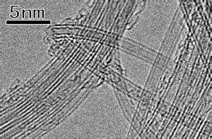
15 Investigating nanotubes Unique surface sensitivity and details at very low voltages Carbon nanotubes with catalyst particles on their surface, imaged at very low energy for best surface details and a HFW of 250nm. Courtesy of Prof. Raynald Gauvin and Camille Probst, Ph.D. Student, McGill University 15
16 Back scattered electrons When an electron from the beam encounters a nucleus in the sample, the resultant Coulomb attraction results in the deflection of the electron's path, known as Rutherford elastic scattering. A few of these electrons will be completely backscattered, re-emerging from the incident surface of the sample. Since the scattering angle is strongly dependent on the atomic number of the nucleus involved, the primary electrons arriving at a given detector position can be used to yield images containing both topological and compositional information.

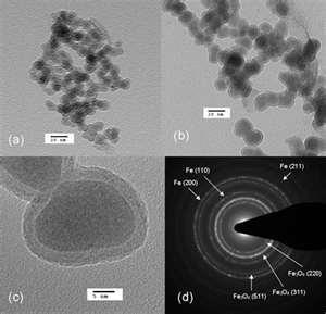
17 Mechanically Activated Composite Nano Particle
18 Energy-Dispersive analysis of X-rays Another possible way in which a beam electron can interact with an atom is by the ionization of an inner shell electron. The resultant vacancy is filled by an outer electron, which can release it's energy by emitting an X-ray. This produces characteristic lines in the X-ray spectrum corresponding to the electronic transitions involved. Since these lines are specific to a given element, the composition of the material can be deduced. This can be used to provide quantitative information about the elements present at a given point on the sample, or alternatively it is possible to map the abundance of a particular element as a function of position.

 L a")
 L b2 (0.2) M x (0.06) L g1 (0.08) M g (0.")
19 Characteristic X-Ray Emission The XEDS detectors can fill and resolve only K,L, and M and a and b lines. Relative Weights of X-ray Lines K a (1) L a (1) M a (1) K b (1) L b1 (0.7) M b (0.6) L b2 (0.2) M x (0.06) L g1 (0.08) M g (0.05) E=hw= hc/l l = 1.24/E(keV)
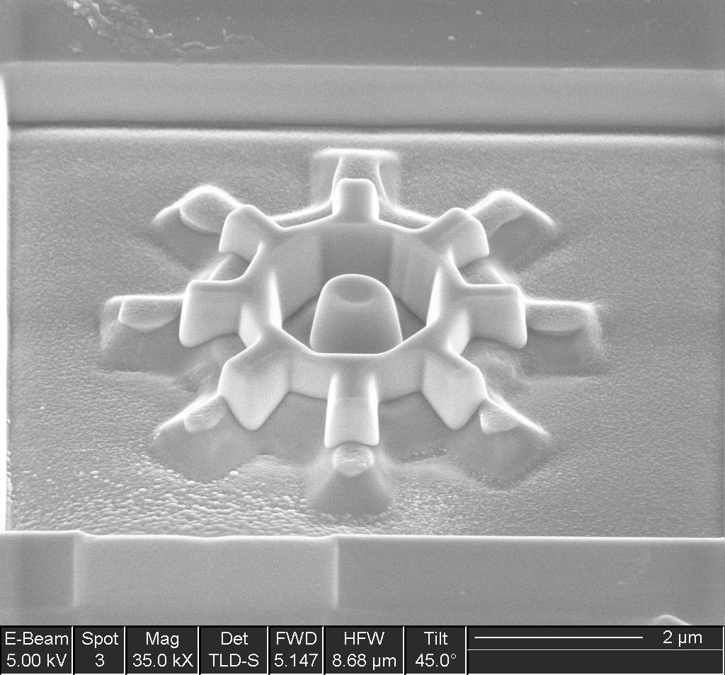
 400")
20 Counts EDX Line Scanning Marker EDX Ni-Al-O Mass Percentage Profile Ni Al O Position (nm)


21 SEM Leo Helps to Understand Martian History Basalts collected from Hawaii: used as Martian analog for acid leaching study Exploring the mechanism for opaline formation from an acid leaching perspective will help to understand its presence on the Martian surface


22 Helios Nano-Lab 600 Dual-Beam Electron Column Ion Column Omni Probe

23 Pushing the Limits for Nano-Work Ultimate Sample Preparation Finer and more automated 2D and 3D Nano-Analysis The best tools for prototyping at the nanoscale


24 Extends to Nano-Analysis in 3D! Collect your data unattended 3D packages handle samples movements and protection to optimize the milling conditions as well as the data acquisition Very large datasets supported Reconstruct and explore in 3D a set of EBSD maps EBS3TM Auto Slice and ViewTM Reconstruct and explore in 3D a tomographic set of cross-sectional images 24

25 Automated Slice and View Ti super Alloy Ti-based superalloy
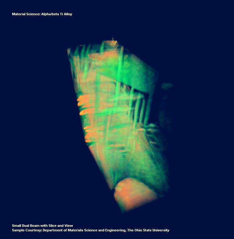
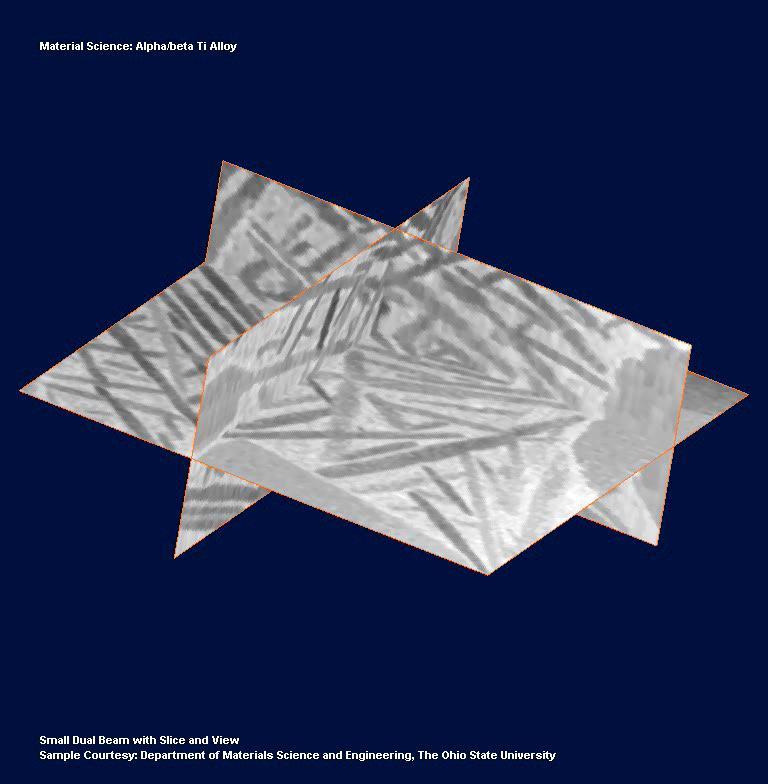
26 Alpha/beta Ti Alloy 3D Reconstruction


27 Advanced Nano Prototyping with FIB Combine the most accurate milling of smallest features, e.g. these sub-20nm lines used in Nano Fluidics HELIOS NANOLAB with the new best FIB milling strategies for fast, redeposition free and smooth sidewalls and write your most advanced functional devices

28 Direct 3D patterning via bmp FIB milling

29 Nano Prototyping: Photonic Array

30 Nano Machining: Micro-indenter (Diamond)


31 FIB Preparation of Atom Probe Tips 10 nm tip diameter

32 Changing Digital e-beam Parameters


33 EBSD: Grain Shape Analysis Electron Backscatter Diffraction Here the direction of the major axis of each ellipse is plotted relative to the horizontal direction Ellipses can be fitted to each grain
34 3D Orientation Maps 2D IPF Map 3D IPF Map

35 3D Grain Selection and Visualization
36 Conclusions There is arguably no other instrument with the breadth of applications in the study of solid materials that compares with the SEM. The SEM is critical in all fields that require characterization of solid materials. Most SEM's are comparatively easy to operate, with user-friendly "intuitive" interfaces. Many applications require minimal sample preparation. For many applications, data acquisition is rapid (less than 5 minutes/image for SEI, BSE, spot EDS analyses.) Modern SEMs generate data in digital formats, which are highly portable. Samples must be solid and they must fit into the microscope chamber. Maximum size in horizontal dimensions is usually on the order of 10 cm, vertical dimensions are generally much more limited and rarely exceed 40 mm. For most instruments samples must be stable in a vacuum on the order of torr. Samples likely to outgas at low pressures are unsuitable for examination in conventional SEM's. However, "low vacuum" and "environmental" SEMs also exist, and many of these types of samples can be successfully examined in these specialized instruments. EDS detectors on SEM's cannot detect very light elements (H, He, and Li). Most SEMs use a solid state x-ray detector (EDS), and while these detectors are very fast and easy to utilize, they have relatively poor energy resolution and sensitivity to elements present in low abundances when compared to wavelength dispersive x-ray detectors (WDS) on most electron probe microanalyzers (EPMA). An electrically conductive coating must be applied to electrically insulating samples for study in conventional SEM's, unless the instrument is capable of operation in a low vacuum mode.
MT Electron microscopy Scanning electron microscopy and electron probe microanalysis
 MT-0.6026 Electron microscopy Scanning electron microscopy and electron probe microanalysis Eero Haimi Research Manager Outline 1. Introduction Basics of scanning electron microscopy (SEM) and electron
Chapter 9. Electron mean free path Microscopy principles of SEM, TEM, LEEM
 Chapter 9 Electron mean free path Microscopy principles of SEM, TEM, LEEM 9.1 Electron Mean Free Path 9. Scanning Electron Microscopy (SEM) -SEM design; Secondary electron imaging; Backscattered electron
Gaetano L Episcopo. Scanning Electron Microscopy Focus Ion Beam and. Pulsed Plasma Deposition
 Gaetano L Episcopo Scanning Electron Microscopy Focus Ion Beam and Pulsed Plasma Deposition Hystorical background Scientific discoveries 1897: J. Thomson discovers the electron. 1924: L. de Broglie propose
Imaging Methods: Scanning Force Microscopy (SFM / AFM)
") Imaging Methods: Scanning Force Microscopy (SFM / AFM) The atomic force microscope (AFM) probes the surface of a sample with a sharp tip, a couple of microns long and often less than 100 Å in diameter.
Imaging Methods: Scanning Force Microscopy (SFM / AFM) The atomic force microscope (AFM) probes the surface of a sample with a sharp tip, a couple of microns long and often less than 100 Å in diameter.
Chapter 12. Nanometrology. Oxford University Press All rights reserved.
 Chapter 12 Nanometrology Introduction Nanometrology is the science of measurement at the nanoscale level. Figure illustrates where nanoscale stands in relation to a meter and sub divisions of meter. Nanometrology
MEMS Metrology. Prof. Tianhong Cui ME 8254
 MEMS Metrology Prof. Tianhong Cui ME 8254 What is metrology? Metrology It is the science of weights and measures Refers primarily to the measurements of length, weight, time, etc. Mensuration- A branch
HOW TO APPROACH SCANNING ELECTRON MICROSCOPY AND ENERGY DISPERSIVE SPECTROSCOPY ANALYSIS. SCSAM Short Course Amir Avishai
 HOW TO APPROACH SCANNING ELECTRON MICROSCOPY AND ENERGY DISPERSIVE SPECTROSCOPY ANALYSIS SCSAM Short Course Amir Avishai RESEARCH QUESTIONS Sea Shell Cast Iron EDS+SE Fe Cr C Objective Ability to ask the
Chapter 10. Nanometrology. Oxford University Press All rights reserved.
 Chapter 10 Nanometrology Oxford University Press 2013. All rights reserved. 1 Introduction Nanometrology is the science of measurement at the nanoscale level. Figure illustrates where nanoscale stands
Basic structure of SEM
 Table of contents Basis structure of SEM SEM imaging modes Comparison of ordinary SEM and FESEM Electron behavior Electron matter interaction o Elastic interaction o Inelastic interaction o Interaction
Everhart-Thornley detector
 SEI Detector Everhart-Thornley detector Microscope chamber wall Faraday cage Scintillator Electrons in Light pipe Photomultiplier Electrical signal out Screen Quartz window +200 V +10 kv Always contains
Electron Microscopy I
 Characterization of Catalysts and Surfaces Characterization Techniques in Heterogeneous Catalysis Electron Microscopy I Introduction Properties of electrons Electron-matter interactions and their applications
object objective lens eyepiece lens
 Advancing Physics G495 June 2015 SET #1 ANSWERS Field and Particle Pictures Seeing with electrons The compound optical microscope Q1. Before attempting this question it may be helpful to review ray diagram
Auger Electron Spectroscopy Overview
 Auger Electron Spectroscopy Overview Also known as: AES, Auger, SAM 1 Auger Electron Spectroscopy E KLL = E K - E L - E L AES Spectra of Cu EdN(E)/dE Auger Electron E N(E) x 5 E KLL Cu MNN Cu LMM E f E
h p λ = mν Back to de Broglie and the electron as a wave you will learn more about this Equation in CHEM* 2060
 Back to de Broglie and the electron as a wave λ = mν h = h p you will learn more about this Equation in CHEM* 2060 We will soon see that the energies (speed for now if you like) of the electrons in the
Nova 600 NanoLab Dual beam Focused Ion Beam IITKanpur
 Nova 600 NanoLab Dual beam Focused Ion Beam system @ IITKanpur Dual Beam Nova 600 Nano Lab From FEI company (Dual Beam = SEM + FIB) SEM: The Electron Beam for SEM Field Emission Electron Gun Energy : 500
EDS User School. Principles of Electron Beam Microanalysis
 EDS User School Principles of Electron Beam Microanalysis Outline 1.) Beam-specimen interactions 2.) EDS spectra: Origin of Bremsstrahlung and characteristic peaks 3.) Moseley s law 4.) Characteristic
Electron probe microanalysis - Electron microprobe analysis EPMA (EMPA) What s EPMA all about? What can you learn?
 What s EPMA all about? What can you learn?") Electron probe microanalysis - Electron microprobe analysis EPMA (EMPA) What s EPMA all about? What can you learn? EPMA - what is it? Precise and accurate quantitative chemical analyses of micron-size
Electron probe microanalysis - Electron microprobe analysis EPMA (EMPA) What s EPMA all about? What can you learn? EPMA - what is it? Precise and accurate quantitative chemical analyses of micron-size
MSE 321 Structural Characterization
 Auger Spectroscopy Auger Electron Spectroscopy (AES) Scanning Auger Microscopy (SAM) Incident Electron Ejected Electron Auger Electron Initial State Intermediate State Final State Physical Electronics
Electron Microprobe Analysis 1 Nilanjan Chatterjee, Ph.D. Principal Research Scientist
 12.141 Electron Microprobe Analysis 1 Nilanjan Chatterjee, Ph.D. Principal Research Scientist Massachusetts Institute of Technology Electron Microprobe Facility Department of Earth, Atmospheric and Planetary
Electron Microprobe Analysis 1 Nilanjan Chatterjee, Ph.D. Principal Research Scientist
 12.141 Electron Microprobe Analysis 1 Nilanjan Chatterjee, Ph.D. Principal Research Scientist Massachusetts Institute of Technology Electron Microprobe Facility Department of Earth, Atmospheric and Planetary
TESCAN S New generation of FIB-SEM microscope
 TESCAN S New generation of FIB-SEM microscope rising standards in sample preparation Key Features SEM COLUMN Versatile system for unlimited applications: resolution imaging (0.9 nm at 15 kev, 1.4 nm at
Dual Beam Helios Nanolab 600 and 650
 Dual Beam Helios Nanolab 600 and 650 In the Clean Room facilities of the INA LMA, several lithography facilities permit to pattern structures at the micro and nano meter scale and to create devices. In
Electron Microprobe Analysis and Scanning Electron Microscopy
 Electron Microprobe Analysis and Scanning Electron Microscopy Electron microprobe analysis (EMPA) Analytical technique in which a beam of electrons is focused on a sample surface, producing X-rays from
Analytical Methods for Materials
 Analytical Methods for Materials Lesson 21 Electron Microscopy and X-ray Spectroscopy Suggested Reading Leng, Chapter 3, pp. 83-126; Chapter 4, pp. 127-160; Chapter 6, pp. 191-219 P.J. Goodhew, J. Humphreys
AP5301/ Name the major parts of an optical microscope and state their functions.
 Review Problems on Optical Microscopy AP5301/8301-2015 1. Name the major parts of an optical microscope and state their functions. 2. Compare the focal lengths of two glass converging lenses, one with
PHYS-E0541:Special Course in Physics Gas phase synthesis of carbon nanotubes for thin film application. Electron Microscopy. for
 PHYS-E0541:Special Course in Physics Gas phase synthesis of carbon nanotubes for thin film application Electron Microscopy for Introduction to Electron Microscopy Carbon Nanomaterials (nanotubes) Dr. Hua
Scanning Electron Microscopy & Ancillary Techniques
 Scanning Electron Microscopy & Ancillary Techniques By Pablo G. Caceres-Valencia The prototype of the first Stereoscan supplied by the Cambridge Instrument Company to the dupont Company, U.S.A. (1965)
MT Electron microscopy Scanning electron microscopy and electron probe microanalysis
 MT-0.6026 Electron microscopy Scanning electron microscopy and electron probe microanalysis Eero Haimi Research Manager Outline 1. Introduction Basics of scanning electron microscopy (SEM) and electron
Massachusetts Institute of Technology. Dr. Nilanjan Chatterjee
 Massachusetts Institute of Technology Dr. Nilanjan Chatterjee Electron Probe Micro-Analysis (EPMA) Imaging and micrometer-scale chemical compositional analysis of solids Signals produced in The Electron
6. Analytical Electron Microscopy
 Physical Principles of Electron Microscopy 6. Analytical Electron Microscopy Ray Egerton University of Alberta and National Institute of Nanotechnology Edmonton, Canada www.tem-eels.ca regerton@ualberta.ca
ECE Semiconductor Device and Material Characterization
 ECE 4813 Semiconductor Device and Material Characterization Dr. Alan Doolittle School of Electrical and Computer Engineering Georgia Institute of Technology As with all of these lecture slides, I am indebted
Modern Optical Spectroscopy
 Modern Optical Spectroscopy X-Ray Microanalysis Shu-Ping Lin, Ph.D. Institute of Biomedical Engineering E-mail: splin@dragon.nchu.edu.tw Website: http://web.nchu.edu.tw/pweb/users/splin/ Backscattered
ABC s of Electrochemistry series Materials Characterization techniques: SEM and EDS Ana María Valenzuela-Muñiz November 3, 2011
 ABC s of Electrochemistry series Materials Characterization techniques: SEM and EDS Ana María Valenzuela-Muñiz November 3, 2011 CEER, Department of Chemical and Biomolecular Engineering Outline Introduction
Overview of scattering, diffraction & imaging in the TEM
 Overview of scattering, diffraction & imaging in the TEM Eric A. Stach Purdue University Scattering Electrons, photons, neutrons Radiation Elastic Mean Free Path (Å)( Absorption Length (Å)( Minimum Probe
Why microscopy?
 Electron Microscopy Why microscopy? http://www.cellsalive.com/howbig.htm 2 Microscopes are used as magnifying tools (although not exclusively as will see later on). The resolution of the human eye is limited
MSE 321 Structural Characterization
 Auger Spectroscopy Auger Electron Spectroscopy (AES) Scanning Auger Microscopy (SAM) Incident Electron Ejected Electron Auger Electron Initial State Intermediate State Final State Physical Electronics
Characterisation of Catalysts Using Secondary and Backscattered Electron In-lens Detectors
 Platinum Metals Rev., 2014, 58, (2), 106 110 FINAL ANALYSIS Characterisation of Catalysts Using Secondary and Backscattered Electron In-lens Detectors Heterogeneous catalysis often involves the use of
Information from Every Angle
 pplication Note Information from Every ngle Directional SE Detector for Next-Level Imaging Zinc oxide nanorods with surficial palladium particles imaged at 500 V in high vacuum. dding palladium increases
= 6 (1/ nm) So what is probability of finding electron tunneled into a barrier 3 ev high?
 So what is probability of finding electron tunneled into a barrier 3 ev high?") STM STM With a scanning tunneling microscope, images of surfaces with atomic resolution can be readily obtained. An STM uses quantum tunneling of electrons to map the density of electrons on the surface
STM STM With a scanning tunneling microscope, images of surfaces with atomic resolution can be readily obtained. An STM uses quantum tunneling of electrons to map the density of electrons on the surface
EE 527 MICROFABRICATION. Lecture 5 Tai-Chang Chen University of Washington
 EE 527 MICROFABRICATION Lecture 5 Tai-Chang Chen University of Washington MICROSCOPY AND VISUALIZATION Electron microscope, transmission electron microscope Resolution: atomic imaging Use: lattice spacing.
Final exam: take-home part
 Final exam: take-home part! List five things that can be done to improve this class. Be specific; give much detail.! (You will be penalized only for insulting comments made for no benefit; you will not
Interactions with Matter
 Manetic Lenses Manetic fields can displace electrons Manetic field can be produced by passin an electrical current throuh coils of wire Manetic field strenth can be increased by usin a soft ferromanetic
SOLID STATE PHYSICS PHY F341. Dr. Manjuladevi.V Associate Professor Department of Physics BITS Pilani
 SOLID STATE PHYSICS PHY F341 Dr. Manjuladevi.V Associate Professor Department of Physics BITS Pilani 333031 manjula@bits-pilani.ac.in Characterization techniques SEM AFM STM BAM Outline What can we use
CHARACTERIZATION of NANOMATERIALS KHP
 CHARACTERIZATION of NANOMATERIALS Overview of the most common nanocharacterization techniques MAIN CHARACTERIZATION TECHNIQUES: 1.Transmission Electron Microscope (TEM) 2. Scanning Electron Microscope
Nanoelectronics 09. Atsufumi Hirohata Department of Electronics. Quick Review over the Last Lecture
 Nanoelectronics 09 Atsufumi Hirohata Department of Electronics 13:00 Monday, 12/February/2018 (P/T 006) Quick Review over the Last Lecture ( Field effect transistor (FET) ): ( Drain ) current increases
Scanning electron microscopy
 Scanning electron microscopy Fei Quanta Tabletop Hitachi Example: Tin soldier Pb M Sn L Secondary electrons Backscatter electrons EDS analysis Average composition Learning goals: Understanding the principle
Scanning Electron Microscopy
 Scanning Electron Microscopy Field emitting tip Grid 2kV 100kV Anode ZEISS SUPRA Variable Pressure FESEM Dr Heath Bagshaw CMA bagshawh@tcd.ie Why use an SEM? Fig 1. Examples of features resolvable using
Low Vacuum Scanning Electron Microscopy and Microanalysis
 Low Vacuum Scanning Electron Microscopy and Microanalysis Principles and Practice of Variable Pressure/Environmental Scanning Electron Microscopy (VP-ESEM), Debbie J Stokes, John Wiley&Sons 2008 Several
Table of Content. Mechanical Removing Techniques. Ultrasonic Machining (USM) Sputtering and Focused Ion Beam Milling (FIB)
 Sputtering and Focused Ion Beam Milling (FIB)") Table of Content Mechanical Removing Techniques Ultrasonic Machining (USM) Sputtering and Focused Ion Beam Milling (FIB) Ultrasonic Machining In ultrasonic machining (USM), also called ultrasonic grinding,
Table of Content Mechanical Removing Techniques Ultrasonic Machining (USM) Sputtering and Focused Ion Beam Milling (FIB) Ultrasonic Machining In ultrasonic machining (USM), also called ultrasonic grinding,
Depth Distribution Functions of Secondary Electron Production and Emission
 Depth Distribution Functions of Secondary Electron Production and Emission Z.J. Ding*, Y.G. Li, R.G. Zeng, S.F. Mao, P. Zhang and Z.M. Zhang Hefei National Laboratory for Physical Sciences at Microscale
Characterization of zeolites by advanced SEM/STEM techniques
 SCIENTIFIC INSTRUMENT NEWS 2016 Vol. 7 SEPTEMBER Technical magazine of Electron Microscope and Analytical Instruments. Article Characterization of zeolites by advanced SEM/STEM techniques Toshiyuki Yokoi
Chemical Analysis in TEM: XEDS, EELS and EFTEM. HRTEM PhD course Lecture 5
 Chemical Analysis in TEM: XEDS, EELS and EFTEM HRTEM PhD course Lecture 5 1 Part IV Subject Chapter Prio x-ray spectrometry 32 1 Spectra and mapping 33 2 Qualitative XEDS 34 1 Quantitative XEDS 35.1-35.4
Ecole Franco-Roumaine : Magnétisme des systèmes nanoscopiques et structures hybrides - Brasov, Modern Analytical Microscopic Tools
 1. Introduction Solid Surfaces Analysis Group, Institute of Physics, Chemnitz University of Technology, Germany 2. Limitations of Conventional Optical Microscopy 3. Electron Microscopies Transmission Electron
Simulation of Ion Beam Etching of Patterned Nanometer-scale Magnetic Structures for High-Density Storage Applications
 Engineered Excellence A Journal for Process and Device Engineers Simulation of Ion Beam Etching of Patterned Nanometer-scale Magnetic Structures for High-Density Storage Applications Introduction Fabrication
Surface Analysis. Dr. Lynn Fuller Dr. Fuller s Webpage:
 ROCHESTER INSTITUTE OF TECHNOLOGY MICROELECTRONIC ENGINEERING Surface Analysis Dr. Lynn Fuller Dr. Fuller s Webpage: http://people.rit.edu/lffeee 82 Lomb Memorial Drive Rochester, NY 14623-5604 Tel (585)
Part II: Thin Film Characterization
 Part II: Thin Film Characterization General details of thin film characterization instruments 1. Introduction to Thin Film Characterization Techniques 2. Structural characterization: SEM, TEM, AFM, STM
Overview of X-Ray Fluorescence Analysis
 Overview of X-Ray Fluorescence Analysis AMPTEK, INC., Bedford, MA 01730 Ph: +1 781 275 2242 Fax: +1 781 275 3470 sales@amptek.com 1 What is X-Ray Fluorescence (XRF)? A physical process: Emission of characteristic
MS482 Materials Characterization ( 재료분석 ) Lecture Note 5: RBS
 Lecture Note 5: RBS") 2016 Fall Semester MS482 Materials Characterization ( 재료분석 ) Lecture Note 5: RBS Byungha Shin Dept. of MSE, KAIST 1 Course Information Syllabus 1. Overview of various characterization techniques (1 lecture)
2016 Fall Semester MS482 Materials Characterization ( 재료분석 ) Lecture Note 5: RBS Byungha Shin Dept. of MSE, KAIST 1 Course Information Syllabus 1. Overview of various characterization techniques (1 lecture)
Energy-Filtering. Transmission. Electron Microscopy
 Part 3 Energy-Filtering Transmission Electron Microscopy 92 Energy-Filtering TEM Principle of EFTEM expose specimen to mono-energetic electron radiation inelastic scattering in the specimen poly-energetic
Geology 777 Monte Carlo Exercise I
 Geology 777 Monte Carlo Exercise I Purpose The goal of this exercise is to get you to think like an electron... to start to think about where electrons from the stream of high energy electrons go when
Nanoscale voxel spectroscopy by simultaneous EELS and EDS tomography
 Electronic Supplementary Material (ESI) for Nanoscale. This journal is The Royal Society of Chemistry 2014 Supplementary Information Nanoscale voxel spectroscopy by simultaneous EELS and EDS tomography
Outlines 3/12/2011. Vacuum Chamber. Inside the sample chamber. Nano-manipulator. Focused ion beam instrument. 1. Other components of FIB instrument
 Focused ion beam instruments Outlines 1. Other components of FIB instrument 1.a Vacuum chamber 1.b Nanomanipulator 1.c Gas supply for deposition 1.d Detectors 2. Capabilities of FIB instrument Lee Chow
ORION NanoFab: An Overview of Applications. White Paper
 ORION NanoFab: An Overview of Applications White Paper ORION NanoFab: An Overview of Applications Author: Dr. Bipin Singh Carl Zeiss NTS, LLC, USA Date: September 2012 Introduction With the advancement
hν' Φ e - Gamma spectroscopy - Prelab questions 1. What characteristics distinguish x-rays from gamma rays? Is either more intrinsically dangerous?
 Gamma spectroscopy - Prelab questions 1. What characteristics distinguish x-rays from gamma rays? Is either more intrinsically dangerous? 2. Briefly discuss dead time in a detector. What factors are important
Praktikum zur. Materialanalytik
 Praktikum zur Materialanalytik Energy Dispersive X-ray Spectroscopy B513 Stand: 19.10.2016 Contents 1 Introduction... 2 2. Fundamental Physics and Notation... 3 2.1. Alignments of the microscope... 3 2.2.
tip conducting surface
 PhysicsAndMathsTutor.com 1 1. The diagram shows the tip of a scanning tunnelling microscope (STM) above a conducting surface. The tip is at a potential of 1.0 V relative to the surface. If the tip is sufficiently
KMÜ 396 MATERIALS SCIENCE AND TECH. I PRESENTATION ELECTRON ENERGY LOSS SPECTROSCOPY (EELS) TUĞÇE SEZGİN
 TUĞÇE SEZGİN") KMÜ 396 MATERIALS SCIENCE AND TECH. I PRESENTATION ELECTRON ENERGY LOSS SPECTROSCOPY (EELS) TUĞÇE SEZGİN 20970725 HACETTEPE UNIVERSITY DEPARTMENT OF CHEMICAL ENGINEERING, SPRING 2011,APRIL,ANKARA CONTENTS
KMÜ 396 MATERIALS SCIENCE AND TECH. I PRESENTATION ELECTRON ENERGY LOSS SPECTROSCOPY (EELS) TUĞÇE SEZGİN 20970725 HACETTEPE UNIVERSITY DEPARTMENT OF CHEMICAL ENGINEERING, SPRING 2011,APRIL,ANKARA CONTENTS
Auger Electron Spectroscopy (AES)
") 1. Introduction Auger Electron Spectroscopy (AES) Silvia Natividad, Gabriel Gonzalez and Arena Holguin Auger Electron Spectroscopy (Auger spectroscopy or AES) was developed in the late 1960's, deriving
1. Introduction Auger Electron Spectroscopy (AES) Silvia Natividad, Gabriel Gonzalez and Arena Holguin Auger Electron Spectroscopy (Auger spectroscopy or AES) was developed in the late 1960's, deriving
Microscopy: Principles
 Low Voltage Electron Microscopy: Principles and Applications Edited by David C. Bell Harvard University, USA and Natasha Erdman JEOL USA Inc., USA Published in association with the Royal Microscopical
ELECTRON MICROSCOPE UNIT
 ELECTRON MICROSCOPE Director: Prof Richard Tilley Associate Director: Dr Nicholas Ariotti Lab Manager: Ms Katie Levick Administrative Assistant: Mr Michael Zhi UNIT Basement Level: F10 Chemical Sciences
Analysis of Insulator Samples with AES
 Analysis of Insulator Samples with AES Kenichi Tsutsumi, Nobuyuki Ikeo, Akihiro Tanaka, and Toyohiko Tazawa SA Business Unit, JEL Ltd. Introduction Auger Electron Spectroscopy (AES) makes it possible to
PHI 5000 Versaprobe-II Focus X-ray Photo-electron Spectroscopy
 PHI 5000 Versaprobe-II Focus X-ray Photo-electron Spectroscopy The very basic theory of XPS XPS theroy Surface Analysis Ultra High Vacuum (UHV) XPS Theory XPS = X-ray Photo-electron Spectroscopy X-ray
CHEM 681 Seminar Mingqi Zhao April 20, 1998 Room 2104, 4:00 p.m. High Resolution Transmission Electron Microscopy: theories and applications
 CHEM 681 Seminar Mingqi Zhao April 20, 1998 Room 2104, 4:00 p.m. High Resolution Transmission Electron Microscopy: theories and applications In materials science, people are always interested in viewing
Auger Electron Spectroscopy
 Auger Electron Spectroscopy Auger Electron Spectroscopy is an analytical technique that provides compositional information on the top few monolayers of material. Detect all elements above He Detection
MSN551 LITHOGRAPHY II
 MSN551 Introduction to Micro and Nano Fabrication LITHOGRAPHY II E-Beam, Focused Ion Beam and Soft Lithography Why need electron beam lithography? Smaller features are required By electronics industry:
MANIPAL INSTITUTE OF TECHNOLOGY
 SCHEME OF EVAUATION MANIPA INSTITUTE OF TECHNOOGY MANIPA UNIVERSITY, MANIPA SECOND SEMESTER B.Tech. END-SEMESTER EXAMINATION - MAY SUBJECT: ENGINEERING PHYSICS (PHY/) Time: 3 Hrs. Max. Marks: 5 Note: Answer
Introduction to EDX. Energy Dispersive X-ray Microanalysis (EDS, Energy dispersive Spectroscopy) Basics of EDX
 Basics of EDX") Introduction to EDX Energy Dispersive X-ray Microanalysis (EDS, Energy dispersive Spectroscopy) EDX Marco Cantoni 1 Basics of EDX a) Generation of X-rays b) Detection Si(Li) Detector, SDD Detector, EDS
Introduction to EDX Energy Dispersive X-ray Microanalysis (EDS, Energy dispersive Spectroscopy) EDX Marco Cantoni 1 Basics of EDX a) Generation of X-rays b) Detection Si(Li) Detector, SDD Detector, EDS
An Introduction to Auger Electron Spectroscopy
 An Introduction to Auger Electron Spectroscopy Spyros Diplas MENA3100 SINTEF Materials & Chemistry, Department of Materials Physics & Centre of Materials Science and Nanotechnology, Department of Chemistry,
Kavli Workshop for Journalists. June 13th, CNF Cleanroom Activities
 Kavli Workshop for Journalists June 13th, 2007 CNF Cleanroom Activities Seeing nm-sized Objects with an SEM Lab experience: Scanning Electron Microscopy Equipment: Zeiss Supra 55VP Scanning electron microscopes
Contrasted strengths and weakness of EDS, WDS and AES for determining the composition of samples
 Contrasted strengths and weakness of EDS, WDS and AES for determining the composition of samples Ana-Marija Nedić Course 590B 12/07/2018 Iowa State University Contrasted strengths and weakness of EDS,
SEM. Chemical Analysis in the. Elastic and Inelastic scattering. Chemical analysis in the SEM. Chemical analysis in the SEM
 THE UNIVERSITY Chemical Analysis in the SEM Ian Jones Centre for Electron Microscopy OF BIRMINGHAM Elastic and Inelastic scattering Electron interacts with one of the orbital electrons Secondary electrons,
POSITRON AND POSITRONIUM INTERACTIONS WITH CONDENSED MATTER. Paul Coleman University of Bath
 POSITRON AND POSITRONIUM INTERACTIONS WITH CONDENSED MATTER Paul Coleman University of Bath THE FATE OF POSITRONS IN CONDENSED MATTER POSITRON-SURFACE INTERACTIONS positron backscattering BACKSCATTERED
Scanning Electron Microscopy
 Scanning Electron Microscopy Amanpreet Kaur 1 www.reading.ac.uk/emlab Scanning Electron Microscopy What is scanning electron microscopy? Basic features of conventional SEM Limitations of conventional SEM
Electron-Matter Interactions
 Electron-Matter Interactions examples of typical EM studies properties of electrons elastic electron-matter interactions scattering processes; coherent and incoherent image formation; chemical contrast;
Introduction to Electron Microscopy Andres Kaech. Instrumentation
 Center for Microscopy and Image Analysis Introduction to Electron Microscopy Andres Kaech Instrumentation The types of electron microscopes Transmission electron microscope (TEM) Scanning electron microscope
Questions/Answers. Chapter 1
 Questions/Answers Chapter 1 1.1 What are the advantages of the SEM over optical microscopy? Advantages: Higher resolution and greater depth of field and microchemical analysis Disadvantages: Expensive,
MS482 Materials Characterization ( 재료분석 ) Lecture Note 4: XRF
 Lecture Note 4: XRF") 2016 Fall Semester MS482 Materials Characterization ( 재료분석 ) Lecture Note 4: XRF Byungha Shin Dept. of MSE, KAIST 1 Course Information Syllabus 1. Overview of various characterization techniques (1 lecture)
2016 Fall Semester MS482 Materials Characterization ( 재료분석 ) Lecture Note 4: XRF Byungha Shin Dept. of MSE, KAIST 1 Course Information Syllabus 1. Overview of various characterization techniques (1 lecture)
FXA UNIT G485 Module X-Rays. Candidates should be able to : I = I 0 e -μx
 1 Candidates should be able to : HISTORY Describe the nature of X-rays. Describe in simple terms how X-rays are produced. X-rays were discovered by Wilhelm Röntgen in 1865, when he found that a fluorescent
Device Characterization of 0.21 µm CMOS Device
 Device Characterization of 0.21 µm CMOS Device Lim Teck Foo 1 *, Ibrahim Ahmad 2 and Muhammad Suhaimi Sulong 3 1 Department of Product Engineering, Altera Corporation. 2 Department of Electrical, Electronics,
EXPERIMENT 5. The Franck-Hertz Experiment (Critical Potentials) Introduction
 Introduction") EXPERIMENT 5 The Franck-Hertz Experiment (Critical Potentials) Introduction In the early part of the twentieth century the structure of the atom was studied in depth. In the process of developing and refining
EXPERIMENT 5 The Franck-Hertz Experiment (Critical Potentials) Introduction In the early part of the twentieth century the structure of the atom was studied in depth. In the process of developing and refining
Writing: Text Types and purposes 1. Write arguments to support claims in an analysis of substantive topics or texts, using valid reasoning and
 Mystery Molecules: Identifying Materials with Nanoscale Characterization Tools Maude Cuchiara (maude_cuchiara@ncsu.edu) Research Triangle Nanotechnology Network Introduction: Novel materials are currently
Secondary Ion Mass Spectrometry (SIMS)
") CHEM53200: Lecture 10 Secondary Ion Mass Spectrometry (SIMS) Major reference: Surface Analysis Edited by J. C. Vickerman (1997). 1 Primary particles may be: Secondary particles can be e s, neutral species
CHEM53200: Lecture 10 Secondary Ion Mass Spectrometry (SIMS) Major reference: Surface Analysis Edited by J. C. Vickerman (1997). 1 Primary particles may be: Secondary particles can be e s, neutral species
The Basic of Transmission Electron Microscope. Text book: Transmission electron microscopy by David B Williams & C. Barry Carter.
 The Basic of Transmission Electron Microscope Text book: Transmission electron microscopy by David B Williams & C. Barry Carter. 2009, Springer Background survey http://presemo.aalto.fi/tem1 Microscopy
Invited Lecture. "Different Aspects of Electron Microscopy. Sardar Vallabhbhai National Institute of Technology, Surat. Deepak Rajput & S.K.
 Invited Lecture on "Different Aspects of Electron Microscopy at Sardar Vallabhbhai National Institute of Technology, Surat Deepak Rajput & S.K. Tiwary R&D and Product Development Essar Steel Limited Abstract
April 10th-12th, 2017
 Thomas LaGrange, Ph.D. Faculty Lecturer and Senior Staff Scientist Introduction: Basics of Transmission Electron Microscopy (TEM) TEM Doctoral Course MS-637 April 10th-12th, 2017 Outline 1. What is microcopy?
Transmission Electron Microscopy
 L. Reimer H. Kohl Transmission Electron Microscopy Physics of Image Formation Fifth Edition el Springer Contents 1 Introduction... 1 1.1 Transmission Electron Microscopy... 1 1.1.1 Conventional Transmission
Developments & Limitations in GSR Analysis
 Developments & Limitations in GSR Analysis ENFSI Working Group Meeting June 2006 Jenny Goulden Oxford Instruments NanoAnalysis Overview Introduction Developments in GSR Software Importance of EDS Hardware
The Franck-Hertz Experiment David Ward The College of Charleston Phys 370/Experimental Physics Spring 1997
 The Franck-Hertz Experiment David Ward The College of Charleston Phys 370/Experimental Physics Spring 1997 Abstract One of the most important experiments supporting quantum theory is the Franck- Hertz
X-RAY PRODUCTION. Prepared by:- EN KAMARUL AMIN BIN ABDULLAH
 X-RAY PRODUCTION Prepared by:- EN KAMARUL AMIN BIN ABDULLAH OBJECTIVES Discuss the process of x-ray being produced (conditions) Explain the principles of energy conversion in x-ray production (how energy
An Anomalous Contrast in Scanning Electron Microscopy of Insulators: The Pseudo Mirror Effect.
 SCANNING VOL., 35-356 (000) Received: March 7, 000 FAMS, Inc. Accepted with revision: August, 000 An Anomalous Contrast in Scanning Electron Microscopy of Insulators: The Pseudo Mirror Effect. M. BELHAJ