h p λ = mν Back to de Broglie and the electron as a wave you will learn more about this Equation in CHEM* 2060
|
|
|
- Lucas Gibson
- 5 years ago
- Views:
Transcription
1 Back to de Broglie and the electron as a wave λ = mν h = h p you will learn more about this Equation in CHEM* 2060 We will soon see that the energies (speed for now if you like) of the electrons in the beams in the microscope are high (v is 70% or more of the speed of light) This definition of mass could be applied in a straightforward way for almost two centuries until Einstein arrived on the scene. In Einstein's theory of motion known as special relativity, the situation became more complicated. When a body is moving, we find that its force acceleration relationship is no longer constant, but depends on two quantities: its speed, and the angle between its direction of motion and the applied force. If we relate the force to the resulting acceleration along each of the three mutually perpendicular spatial axes, we find that in each of the three expressions a factor of γ m appears, where the gamma factor γ = (1 v 2 /c 2 ) 1/2 is a common quantity in special relativity, and m is the body's rest mass. The new quantity γ m is traditionally called the body's relativistic mass. ( Is called the Lorentz factor (see page 123 of text) Bottom line: this will change the wavelength of the electron 3-1
2 So we modify the wavelength according to 8 = h/p = h/(mv 8 = (h/mv)* r(1- v 2 /c 2 ) The wavelength is also given by a somewhat simpler ploy.. KE = ½ mv 2 = E But h/8 = mv and so (h/8) 2 = (mv) 2 = p 2 2mE = m 2 v 2 = p 2 h 2 /8 2 = 2mE 8 2 = h 2 /2mE 8 = h / r(2me) See eqn
 Exactly what you want or what you see depends on man Experimental factors Lets see what this all means")
3 Electrons and their interaction with matter electrons interact with matter in many ways can be scattered once or more that once elastic or inelastic effects can be used for imaging or to get other info (see later) Exactly what you want or what you see depends on man Experimental factors Lets see what this all means 3-3
4 Types of electrons that come off the sample and how they are useful 1. Secondary Electrons Secondary electrons are electrons generated as ionization products. They are called 'secondary' because they are generated by other radiation (the primary radiation). This radiation can be in the form of ions, electrons, or photons with sufficiently high energy, i.e. exceeding the ionization potential. Mean free path of low-energy electrons. Secondary electrons are generally considered to have energies below 50 ev. The rate of energy loss for electron scattering is very low, so most electrons released have energies peaking below 5 ev(seiler, 1983). Secondary electrons are also the main means of viewing images in the SEM. The range of secondary electrons depends on the energy. The distance they originate from is on the order of a few nanometers in metals and tens of nanometers in insulators This small distance allows such fine resolution to be achieved in the SEM. 3-4

5 Notice how the depth from which the electrons originate is small Usually gives large depth of field -image is clean 3-5

6 2. Backscattered Electrons Backscattered electrons (BSE) consist of high-energy electrons originating in the electron beam, that are reflected or back-scattered out of the specimen interaction volume by elastic interactions with specimen atoms. Since heavy elements (high atomic number) backscatter electrons more strongly than light elements (low atomic number), and thus appear brighter in the image, BSE are used to detect contrast between areas with different chemical compositions. The image illustrates two different scanning modes of a scanning electron microscope (SEM). In the lower part of the image, we can see the relief of the sample. This is obtained using the detection of secondary electrons. In the upper part of the image, we can see light spots surrounded by darker areas. The light spots correspond to the zirconium aggregates in an aluminum matrix. This is obtained using the detection of backscattered electrons. 3-6
7 3. Surface Plasmons: don t worry about these: not used in SEM 4. Auger Electrons: also we will not learn about the Auger effect here 5. Bremsstrahlung Radiation The word Bremsstrahlung is retained from the original German to describe the radiation which is emitted when electrons are decelerated or "braked" when they are fired at a metal target. Accelerated charges give off electromagnetic radiation, and when the energy of the bombarding electrons is high enough, that radiation is in the x-ray region of the electromagnetic spectrum. It is characterized by a continuous distribution of radiation which becomes more intense and shifts toward higher frequencies when the energy of the bombarding electrons is increased. Considered to be background radiation 3-7

8 6. Cathode Ray Luminescence -- cathodoluminescence Cathodoluminescence occurs when a beam of electrons (30kV or so) impacts on a luminescent material such as a phosphor causing the material to emit visible light. The most common example is the screen of a tv. In geology, mineralogy and materials science SEM with specialized optical detectors, or an optical is used to examine internal structures of semiconductors, rocks, ceramic, glass etc. in order to get information on the composition, growth and quality of the material. CL image of a granite sample 3-8
 are about 100kV. Transmission efficiency is Inversely proportional to thickness (so thin samples are best).")
9 7. Transmitted unscattered electrons This is the basis for TEM (see a bit later). There is no interaction between the electrons and the sample. The acceleration voltages (see electron guns soon) are about 100kV. Transmission efficiency is Inversely proportional to thickness (so thin samples are best). Light elements transmit better and appear Light on detection screen and the reverse is true for heavy elements. Highest resolution good for nano!! 3-9


10 Scanning Electron Microscopy (SEM) As we know the Scanning Electron Microscope (SEM) is a microscope that uses electrons rather than light to form an image. Advantages: SEM instead of a light microscope. SEM has a large depth of field, which allows a large amount of the sample to be in focus at one time. produces images of high resolution, which means that closely spaced features can be examined at a high magnification. Preparation of the samples is relatively easy since most SEMs only require the sample to be conductive. The combination of higher magnification, larger depth of focus, greater resolution, and ease of sample observation makes the SEM one of the most heavily used instruments in research areas today. Amorphous SiOx nanowire bundles have an uncanny ability to self-assemble into various shapes, including one that strikingly resembles a sunflower. Each nanowire is about 10 nm in diameter 3-10

, so more thermal energy LaB 6 ; and Ce 6")
 negative relative to ground, so")
11 First we look at the instrument itself Electrons are produced by a hot filament like a flashlight bulb Electrodes connect to power Tungsten filament Ceramic insulator heated wire gives electrons enough thermal energy to overcome work function of the source, with an electric potential to give electrons a direction and velocity. materials used for source are Tungsten (has a very high melting temp), so more thermal energy LaB 6 ; and Ce 6 (have a low work function and a high melting temp.). source is usually held at some potential (anywhere from ~500V to maybe 100kV) negative relative to ground, so that a sample (as well as the rest of the microscope) can be kept at 3-11 ground.


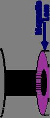

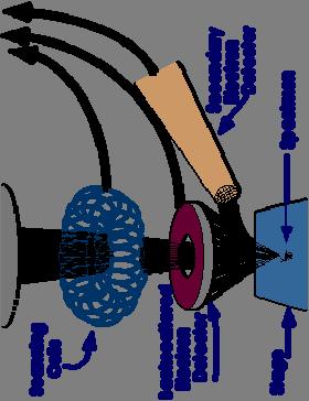
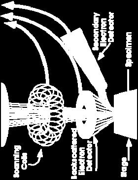
12 Electron optics (also see Fig 3.6) Sample goes here 3-12


13 Image Generation Images are collected by rastering the electron beam (spot size 50 microns or less) Across the sample. The electrons that bounce off the sample are sent to a detector This signal is sent to a display which is scanned synchronously Detectors collect these X-rays, backscattered electrons, and secondary electrons and convert them into a signal that is sent to a screen similar to a television screen. Images are photographed or stored digitally 3-13


14 SEM-EDX (Electron Probe Microanalysis) X Ray Fluorescence Spectrum image 3-14
15 X-Ray emission When very energetic (fast) electrons hit a sample X rays are given off Electrons knocked out of atoms sample Incoming electrons 3-15
MT Electron microscopy Scanning electron microscopy and electron probe microanalysis
 MT-0.6026 Electron microscopy Scanning electron microscopy and electron probe microanalysis Eero Haimi Research Manager Outline 1. Introduction Basics of scanning electron microscopy (SEM) and electron
object objective lens eyepiece lens
 Advancing Physics G495 June 2015 SET #1 ANSWERS Field and Particle Pictures Seeing with electrons The compound optical microscope Q1. Before attempting this question it may be helpful to review ray diagram
Electron Microprobe Analysis and Scanning Electron Microscopy
 Electron Microprobe Analysis and Scanning Electron Microscopy Electron microprobe analysis (EMPA) Analytical technique in which a beam of electrons is focused on a sample surface, producing X-rays from
Electron Microscopy I
 Characterization of Catalysts and Surfaces Characterization Techniques in Heterogeneous Catalysis Electron Microscopy I Introduction Properties of electrons Electron-matter interactions and their applications
Nano-Microscopy. Lecture 2. Scanning and Transmission Electron Microscopies: Principles. Pavel Zinin HIGP, University of Hawaii, Honolulu, USA
 GG 711: Advanced Techniques in Geophysics and Materials Science Nano-Microscopy. Lecture 2 Scanning and Transmission Electron Microscopies: Principles Pavel Zinin HIGP, University of Hawaii, Honolulu,
Chapter 10: Wave Properties of Particles
 Chapter 10: Wave Properties of Particles Particles such as electrons may demonstrate wave properties under certain conditions. The electron microscope uses these properties to produce magnified images
Ecole Franco-Roumaine : Magnétisme des systèmes nanoscopiques et structures hybrides - Brasov, Modern Analytical Microscopic Tools
 1. Introduction Solid Surfaces Analysis Group, Institute of Physics, Chemnitz University of Technology, Germany 2. Limitations of Conventional Optical Microscopy 3. Electron Microscopies Transmission Electron
Gaetano L Episcopo. Scanning Electron Microscopy Focus Ion Beam and. Pulsed Plasma Deposition
 Gaetano L Episcopo Scanning Electron Microscopy Focus Ion Beam and Pulsed Plasma Deposition Hystorical background Scientific discoveries 1897: J. Thomson discovers the electron. 1924: L. de Broglie propose
Imaging Methods: Scanning Force Microscopy (SFM / AFM)
") Imaging Methods: Scanning Force Microscopy (SFM / AFM) The atomic force microscope (AFM) probes the surface of a sample with a sharp tip, a couple of microns long and often less than 100 Å in diameter.
Imaging Methods: Scanning Force Microscopy (SFM / AFM) The atomic force microscope (AFM) probes the surface of a sample with a sharp tip, a couple of microns long and often less than 100 Å in diameter.
EDS User School. Principles of Electron Beam Microanalysis
 EDS User School Principles of Electron Beam Microanalysis Outline 1.) Beam-specimen interactions 2.) EDS spectra: Origin of Bremsstrahlung and characteristic peaks 3.) Moseley s law 4.) Characteristic
Electron Microprobe Analysis 1 Nilanjan Chatterjee, Ph.D. Principal Research Scientist
 12.141 Electron Microprobe Analysis 1 Nilanjan Chatterjee, Ph.D. Principal Research Scientist Massachusetts Institute of Technology Electron Microprobe Facility Department of Earth, Atmospheric and Planetary
Electron Microprobe Analysis 1 Nilanjan Chatterjee, Ph.D. Principal Research Scientist
 12.141 Electron Microprobe Analysis 1 Nilanjan Chatterjee, Ph.D. Principal Research Scientist Massachusetts Institute of Technology Electron Microprobe Facility Department of Earth, Atmospheric and Planetary
Basic structure of SEM
 Table of contents Basis structure of SEM SEM imaging modes Comparison of ordinary SEM and FESEM Electron behavior Electron matter interaction o Elastic interaction o Inelastic interaction o Interaction
Transmission Electron Microscopy
 L. Reimer H. Kohl Transmission Electron Microscopy Physics of Image Formation Fifth Edition el Springer Contents 1 Introduction... 1 1.1 Transmission Electron Microscopy... 1 1.1.1 Conventional Transmission
Invited Lecture. "Different Aspects of Electron Microscopy. Sardar Vallabhbhai National Institute of Technology, Surat. Deepak Rajput & S.K.
 Invited Lecture on "Different Aspects of Electron Microscopy at Sardar Vallabhbhai National Institute of Technology, Surat Deepak Rajput & S.K. Tiwary R&D and Product Development Essar Steel Limited Abstract
Electron-Matter Interactions
 Electron-Matter Interactions examples of typical EM studies properties of electrons elastic electron-matter interactions scattering processes; coherent and incoherent image formation; chemical contrast;
Massachusetts Institute of Technology. Dr. Nilanjan Chatterjee
 Massachusetts Institute of Technology Dr. Nilanjan Chatterjee Electron Probe Micro-Analysis (EPMA) Imaging and micrometer-scale chemical compositional analysis of solids Signals produced in The Electron
Scanning Electron Microscopy & Ancillary Techniques
 Scanning Electron Microscopy & Ancillary Techniques By Pablo G. Caceres-Valencia The prototype of the first Stereoscan supplied by the Cambridge Instrument Company to the dupont Company, U.S.A. (1965)
FXA UNIT G485 Module X-Rays. Candidates should be able to : I = I 0 e -μx
 1 Candidates should be able to : HISTORY Describe the nature of X-rays. Describe in simple terms how X-rays are produced. X-rays were discovered by Wilhelm Röntgen in 1865, when he found that a fluorescent
= 6 (1/ nm) So what is probability of finding electron tunneled into a barrier 3 ev high?
 So what is probability of finding electron tunneled into a barrier 3 ev high?") STM STM With a scanning tunneling microscope, images of surfaces with atomic resolution can be readily obtained. An STM uses quantum tunneling of electrons to map the density of electrons on the surface
STM STM With a scanning tunneling microscope, images of surfaces with atomic resolution can be readily obtained. An STM uses quantum tunneling of electrons to map the density of electrons on the surface
Scanning Electron Microscopy
 Scanning Electron Microscopy Field emitting tip Grid 2kV 100kV Anode ZEISS SUPRA Variable Pressure FESEM Dr Heath Bagshaw CMA bagshawh@tcd.ie Why use an SEM? Fig 1. Examples of features resolvable using
Chemical Analysis in TEM: XEDS, EELS and EFTEM. HRTEM PhD course Lecture 5
 Chemical Analysis in TEM: XEDS, EELS and EFTEM HRTEM PhD course Lecture 5 1 Part IV Subject Chapter Prio x-ray spectrometry 32 1 Spectra and mapping 33 2 Qualitative XEDS 34 1 Quantitative XEDS 35.1-35.4
Why microscopy?
 Electron Microscopy Why microscopy? http://www.cellsalive.com/howbig.htm 2 Microscopes are used as magnifying tools (although not exclusively as will see later on). The resolution of the human eye is limited
AP5301/ Name the major parts of an optical microscope and state their functions.
 Review Problems on Optical Microscopy AP5301/8301-2015 1. Name the major parts of an optical microscope and state their functions. 2. Compare the focal lengths of two glass converging lenses, one with
X-RAY PRODUCTION. Prepared by:- EN KAMARUL AMIN BIN ABDULLAH
 X-RAY PRODUCTION Prepared by:- EN KAMARUL AMIN BIN ABDULLAH OBJECTIVES Discuss the process of x-ray being produced (conditions) Explain the principles of energy conversion in x-ray production (how energy
Practical course in scanning electron microscopy
 Practical course in scanning electron microscopy Fortgeschrittenen Praktikum an der Technischen Universität München Wintersemester 2017/2018 Table of contents 1. Introduction 3 2. Formation of an electron
Interactions with Matter
 Manetic Lenses Manetic fields can displace electrons Manetic field can be produced by passin an electrical current throuh coils of wire Manetic field strenth can be increased by usin a soft ferromanetic
Chapter 9. Electron mean free path Microscopy principles of SEM, TEM, LEEM
 Chapter 9 Electron mean free path Microscopy principles of SEM, TEM, LEEM 9.1 Electron Mean Free Path 9. Scanning Electron Microscopy (SEM) -SEM design; Secondary electron imaging; Backscattered electron
SEM Optics and Application to Current Research
 SEM Optics and Application to Current Research Azure Avery May 28, 2008 1 Introduction 1.1 History The optical microscope was invented in the early 17th century. Although revolutionary, the earliest microscopes
M2 TP. Low-Energy Electron Diffraction (LEED)
") M2 TP Low-Energy Electron Diffraction (LEED) Guide for report preparation I. Introduction: Elastic scattering or diffraction of electrons is the standard technique in surface science for obtaining structural
M2 TP Low-Energy Electron Diffraction (LEED) Guide for report preparation I. Introduction: Elastic scattering or diffraction of electrons is the standard technique in surface science for obtaining structural
Modern Optical Spectroscopy
 Modern Optical Spectroscopy X-Ray Microanalysis Shu-Ping Lin, Ph.D. Institute of Biomedical Engineering E-mail: splin@dragon.nchu.edu.tw Website: http://web.nchu.edu.tw/pweb/users/splin/ Backscattered
Part II: Thin Film Characterization
 Part II: Thin Film Characterization General details of thin film characterization instruments 1. Introduction to Thin Film Characterization Techniques 2. Structural characterization: SEM, TEM, AFM, STM
SEM stands for Scanning Electron Microscopy. The earliest known work describing
 1. HISTORY ABOUT SEM SEM stands for Scanning Electron Microscopy. The earliest known work describing the concept of a Scanning Electron Microscope was by M. Knoll (1935) who, along with other pioneers
Revision Guide. Chapter 7 Quantum Behaviour
 Revision Guide Chapter 7 Quantum Behaviour Contents CONTENTS... 2 REVISION CHECKLIST... 3 REVISION NOTES... 4 QUANTUM BEHAVIOUR... 4 Random arrival of photons... 4 Photoelectric effect... 5 PHASE AN PHASORS...
tip conducting surface
 PhysicsAndMathsTutor.com 1 1. The diagram shows the tip of a scanning tunnelling microscope (STM) above a conducting surface. The tip is at a potential of 1.0 V relative to the surface. If the tip is sufficiently
4. Inelastic Scattering
 1 4. Inelastic Scattering Some inelastic scattering processes A vast range of inelastic scattering processes can occur during illumination of a specimen with a highenergy electron beam. In principle, many
Analytical Methods for Materials
 Analytical Methods for Materials Lesson 21 Electron Microscopy and X-ray Spectroscopy Suggested Reading Leng, Chapter 3, pp. 83-126; Chapter 4, pp. 127-160; Chapter 6, pp. 191-219 P.J. Goodhew, J. Humphreys
April 10th-12th, 2017
 Thomas LaGrange, Ph.D. Faculty Lecturer and Senior Staff Scientist Introduction: Basics of Transmission Electron Microscopy (TEM) TEM Doctoral Course MS-637 April 10th-12th, 2017 Outline 1. What is microcopy?
Paper 2. Section B : Atomic World
 Paper 2 Section B : Atomic World Q.2 Multiple-choice questions A B C D 2.1 25.19 15.78 9.18 49.68 2.2 25.79 20.39 41.97 11.72 2.3 18.35 9.76 48.84 22.65 2.4 9.27 18.87 27.90 43.50 2.5 63.47 4.28 10.99
Production of X-rays. Radiation Safety Training for Analytical X-Ray Devices Module 9
 Module 9 This module presents information on what X-rays are and how they are produced. Introduction Module 9, Page 2 X-rays are a type of electromagnetic radiation. Other types of electromagnetic radiation
ABC s of Electrochemistry series Materials Characterization techniques: SEM and EDS Ana María Valenzuela-Muñiz November 3, 2011
 ABC s of Electrochemistry series Materials Characterization techniques: SEM and EDS Ana María Valenzuela-Muñiz November 3, 2011 CEER, Department of Chemical and Biomolecular Engineering Outline Introduction
Introduction to Electron Microscopy Andres Kaech. Instrumentation
 Center for Microscopy and Image Analysis Introduction to Electron Microscopy Andres Kaech Instrumentation The types of electron microscopes Transmission electron microscope (TEM) Scanning electron microscope
CBE Science of Engineering Materials. Scanning Electron Microscopy (SEM)
") CBE 30361 Science of Engineering Materials Scanning Electron Microscopy (SEM) Scale of Structure Organization Units: micrometer = 10-6 m = 1µm nanometer= 10-9 m = 1nm Angstrom = 10-10 m = 1Å A hair is
CBE 30361 Science of Engineering Materials Scanning Electron Microscopy (SEM) Scale of Structure Organization Units: micrometer = 10-6 m = 1µm nanometer= 10-9 m = 1nm Angstrom = 10-10 m = 1Å A hair is
Characterisation of Catalysts Using Secondary and Backscattered Electron In-lens Detectors
 Platinum Metals Rev., 2014, 58, (2), 106 110 FINAL ANALYSIS Characterisation of Catalysts Using Secondary and Backscattered Electron In-lens Detectors Heterogeneous catalysis often involves the use of
Auger Electron Spectroscopy Overview
 Auger Electron Spectroscopy Overview Also known as: AES, Auger, SAM 1 Auger Electron Spectroscopy E KLL = E K - E L - E L AES Spectra of Cu EdN(E)/dE Auger Electron E N(E) x 5 E KLL Cu MNN Cu LMM E f E
Electron Diffraction
 Electron iffraction o moving electrons display wave nature? To answer this question you will direct a beam of electrons through a thin layer of carbon and analyze the resulting pattern. Theory Louis de
What can laser light do for (or to) me?
 me?") What can laser light do for (or to) me? Phys 1020, Day 15: Questions? Refection, refraction LASERS: 14.3 Next Up: Finish lasers Cameras and optics 1 Eyes to web: Final Project Info Light travels more slowly
What can laser light do for (or to) me? Phys 1020, Day 15: Questions? Refection, refraction LASERS: 14.3 Next Up: Finish lasers Cameras and optics 1 Eyes to web: Final Project Info Light travels more slowly
HOW TO APPROACH SCANNING ELECTRON MICROSCOPY AND ENERGY DISPERSIVE SPECTROSCOPY ANALYSIS. SCSAM Short Course Amir Avishai
 HOW TO APPROACH SCANNING ELECTRON MICROSCOPY AND ENERGY DISPERSIVE SPECTROSCOPY ANALYSIS SCSAM Short Course Amir Avishai RESEARCH QUESTIONS Sea Shell Cast Iron EDS+SE Fe Cr C Objective Ability to ask the
Sound wave bends as it hits an interface at an oblique angle. 4. Reflection. Sound wave bounces back to probe
 : Ultrasound imaging and x-rays 1. How does ultrasound imaging work?. What is ionizing electromagnetic radiation? Definition of ionizing radiation 3. How are x-rays produced? Bremsstrahlung Auger electron
Electron probe microanalysis - Electron microprobe analysis EPMA (EMPA) What s EPMA all about? What can you learn?
 What s EPMA all about? What can you learn?") Electron probe microanalysis - Electron microprobe analysis EPMA (EMPA) What s EPMA all about? What can you learn? EPMA - what is it? Precise and accurate quantitative chemical analyses of micron-size
Electron probe microanalysis - Electron microprobe analysis EPMA (EMPA) What s EPMA all about? What can you learn? EPMA - what is it? Precise and accurate quantitative chemical analyses of micron-size
Electron beam scanning
 Electron beam scanning The Electron beam scanning operates through an electro-optical system which has the task of deflecting the beam Synchronously with cathode ray tube which create the image, beam moves
6. Analytical Electron Microscopy
 Physical Principles of Electron Microscopy 6. Analytical Electron Microscopy Ray Egerton University of Alberta and National Institute of Nanotechnology Edmonton, Canada www.tem-eels.ca regerton@ualberta.ca
Semiconductor Physics and Devices
 Introduction to Quantum Mechanics In order to understand the current-voltage characteristics, we need some knowledge of electron behavior in semiconductor when the electron is subjected to various potential
Lecture 2: Quantum Mechanics and Relativity
 Lecture 2: Quantum Mechanics and Relativity Atom Atomic number A Number of protons Z Number of neutrons A-Z Number of electrons Z Charge of electron = charge of proton ~1.6 10-19 C Size of the atom ~10-10
Chapter 38. Photons Light Waves Behaving as Particles
 Chapter 38 Photons Light Waves Behaving as Particles 38.1 The Photoelectric Effect The photoelectric effect was first discovered by Hertz in 1887, and was explained by Einstein in 1905. The photoelectric
Techniques EDX, EELS et HAADF en TEM: possibilités d analyse et applications
 Techniques EDX, EELS et HAADF en TEM: possibilités d analyse et applications Thomas Neisius Université Paul Cézanne Plan Imaging modes HAADF Example: supported Pt nanoparticles Electron sample interaction
Chapter Six: X-Rays. 6.1 Discovery of X-rays
 Chapter Six: X-Rays 6.1 Discovery of X-rays In late 1895, a German physicist, W. C. Roentgen was working with a cathode ray tube in his laboratory. He was working with tubes similar to our fluorescent
The Franck-Hertz Experiment Physics 2150 Experiment No. 9 University of Colorado
 Experiment 9 1 Introduction The Franck-Hertz Experiment Physics 2150 Experiment No. 9 University of Colorado During the late nineteenth century, a great deal of evidence accumulated indicating that radiation
Basic physics Questions
 Chapter1 Basic physics Questions S. Ilyas 1. Which of the following statements regarding protons are correct? a. They have a negative charge b. They are equal to the number of electrons in a non-ionized
Lecture 5: Characterization methods
 Lecture 5: Characterization methods X-Ray techniques Single crystal X-Ray Diffration (XRD) Powder XRD Thin film X-Ray Reflection (XRR) Microscopic methods Optical microscopy Electron microscopies (SEM,
PhysicsAndMathsTutor.com 1
 PhysicsAndMathsTutor.com 1 1. Millikan determined the charge on individual oil droplets using an arrangement as represented in the diagram. The plate voltage necessary to hold a charged droplet stationary
1 P a g e h t t p s : / / w w w. c i e n o t e s. c o m / Physics (A-level)
") 1 P a g e h t t p s : / / w w w. c i e n o t e s. c o m / Physics (A-level) Electromagnetic induction (Chapter 23): For a straight wire, the induced current or e.m.f. depends on: The magnitude of the magnetic
1 P a g e h t t p s : / / w w w. c i e n o t e s. c o m / Physics (A-level) Electromagnetic induction (Chapter 23): For a straight wire, the induced current or e.m.f. depends on: The magnitude of the magnetic
[2] (b) An electron is accelerated from rest through a potential difference of 300 V.
![[2] (b) An electron is accelerated from rest through a potential difference of 300 V.](/thumbs/89/98791036.jpg "[2] (b) An electron is accelerated from rest through a potential difference of 300 V.") 1 (a) In atomic physics electron energies are often stated in electronvolts (ev) Define the electronvolt. State its value in joule.. [2] (b) An electron is accelerated from rest through a potential difference
1 (a) In atomic physics electron energies are often stated in electronvolts (ev) Define the electronvolt. State its value in joule.. [2] (b) An electron is accelerated from rest through a potential difference
Auger Electron Spectroscopy
 Auger Electron Spectroscopy Auger Electron Spectroscopy is an analytical technique that provides compositional information on the top few monolayers of material. Detect all elements above He Detection
PHYS-E0541:Special Course in Physics Gas phase synthesis of carbon nanotubes for thin film application. Electron Microscopy. for
 PHYS-E0541:Special Course in Physics Gas phase synthesis of carbon nanotubes for thin film application Electron Microscopy for Introduction to Electron Microscopy Carbon Nanomaterials (nanotubes) Dr. Hua
Chapter 37 Early Quantum Theory and Models of the Atom
 Chapter 37 Early Quantum Theory and Models of the Atom Units of Chapter 37 37-7 Wave Nature of Matter 37-8 Electron Microscopes 37-9 Early Models of the Atom 37-10 Atomic Spectra: Key to the Structure
Praktikum zur. Materialanalytik
 Praktikum zur Materialanalytik Energy Dispersive X-ray Spectroscopy B513 Stand: 19.10.2016 Contents 1 Introduction... 2 2. Fundamental Physics and Notation... 3 2.1. Alignments of the microscope... 3 2.2.
Everhart-Thornley detector
 SEI Detector Everhart-Thornley detector Microscope chamber wall Faraday cage Scintillator Electrons in Light pipe Photomultiplier Electrical signal out Screen Quartz window +200 V +10 kv Always contains
The Wave Nature of Matter *
 OpenStax-CNX module: m42576 1 The Wave Nature of Matter * OpenStax This work is produced by OpenStax-CNX and licensed under the Creative Commons Attribution License 3.0 Abstract Describe the Davisson-Germer
QUANTUM PHYSICS. Limitation: This law holds well only for the short wavelength and not for the longer wavelength. Raleigh Jean s Law:
 Black body: A perfect black body is one which absorbs all the radiation of heat falling on it and emits all the radiation when heated in an isothermal enclosure. The heat radiation emitted by the black
PHI 5000 Versaprobe-II Focus X-ray Photo-electron Spectroscopy
 PHI 5000 Versaprobe-II Focus X-ray Photo-electron Spectroscopy The very basic theory of XPS XPS theroy Surface Analysis Ultra High Vacuum (UHV) XPS Theory XPS = X-ray Photo-electron Spectroscopy X-ray
Auger Electron Spectroscopy (AES) Prof. Paul K. Chu
 Prof. Paul K. Chu") Auger Electron Spectroscopy (AES) Prof. Paul K. Chu Auger Electron Spectroscopy Introduction Principles Instrumentation Qualitative analysis Quantitative analysis Depth profiling Mapping Examples The Auger
Auger Electron Spectroscopy (AES) Prof. Paul K. Chu Auger Electron Spectroscopy Introduction Principles Instrumentation Qualitative analysis Quantitative analysis Depth profiling Mapping Examples The Auger
Chapter 6. Fiber Optic Thermometer. Ho Suk Ryou
 Chapter 6. Fiber Optic Thermometer Ho Suk Ryou Properties of Optical Fiber Optical Fiber Composed of rod core surrounded by sheath Core: conducts electromagnetic wave Sheath: contains wave within the core
Electron and electromagnetic radiation
 Electron and electromagnetic radiation Generation and interactions with matter Stimuli Interaction with sample Response Stimuli Waves and energy The energy is propotional to 1/λ and 1/λ 2 λ λ 1 Electromagnetic
MSE 321 Structural Characterization
 Optical Microscope Plan Lenses In an "ideal" single-element lens system all planar wave fronts are focused to a point at distance f from the lens; therefore: Image near the optical axis will be in perfect
CHAPTER 3 The Experimental Basis of Quantum Theory
 CHAPTER 3 The Experimental Basis of Quantum Theory 3.1 3.2 3.3 3.4 3.5 3.6 3.7 3.8 3.9 Discovery of the X Ray and the Electron Determination of Electron Charge Line Spectra Quantization As far as I can
ELECTROMAGNETIC WAVES
 VISUAL PHYSICS ONLINE MODULE 7 NATURE OF LIGHT ELECTROMAGNETIC WAVES SPECTRA PRODUCED BY DISCHARGE TUBES CATHODE RAYS (electron beams) Streams of electrons (negatively charged particles) observed in vacuum
Quantum physics. Anyone who is not shocked by the quantum theory has not understood it. Niels Bohr, Nobel Price in 1922 ( )
") Quantum physics Anyone who is not shocked by the quantum theory has not understood it. Niels Bohr, Nobel Price in 1922 (1885-1962) I can safely say that nobody understand quantum physics Richard Feynman
Quantum physics Anyone who is not shocked by the quantum theory has not understood it. Niels Bohr, Nobel Price in 1922 (1885-1962) I can safely say that nobody understand quantum physics Richard Feynman
Scanning electron microscopy
 Scanning electron microscopy Fei Quanta Tabletop Hitachi Example: Tin soldier Pb M Sn L Secondary electrons Backscatter electrons EDS analysis Average composition Learning goals: Understanding the principle
Classical and Planck picture. Planck s constant. Question. Quantum explanation for the Wein Effect.
 6.1 Quantum Physics. Particle Nature of Light Particle nature of Light Blackbody Radiation Photoelectric Effect Properties of photons Ionizing radiation Radiation damage x-rays Compton effect X-ray diffraction
SOLID STATE PHYSICS PHY F341. Dr. Manjuladevi.V Associate Professor Department of Physics BITS Pilani
 SOLID STATE PHYSICS PHY F341 Dr. Manjuladevi.V Associate Professor Department of Physics BITS Pilani 333031 manjula@bits-pilani.ac.in Characterization techniques SEM AFM STM BAM Outline What can we use
Introduction to Electron Beam Lithography
 Introduction to Electron Beam Lithography Boštjan Berčič (bostjan.bercic@ijs.si), Jožef Štefan Institute, Jamova 39, 1000 Ljubljana, Slovenia 1. Introduction Electron Beam Lithography is a specialized
Chapter 28: Quantum Physics. Don t Copy This. Quantum Physics 3/16/13
 Chapter 28: Quantum Physics Key Terms: Photoelectric effect Photons de Broglie wavelength Energy level diagram Wave-particle duality Don t Copy This Except for relativity, everything we have studied up
The illumination source: the electron beam
 The SEM Column The illumination source: the electron beam The probe of the electron microscope is an electron beam with very high and stable energy (10-100 kev) in order to get images with high resolution.
Title / paragraph example Topic: Quantum Computers. Course essay. Photoelectric effect summary. From Last Time. Photon interference?
 Course essay Friday, Nov 3: Due in class essay topic(review article, operating experiment, noble prize) short description - one paragraph http://www.hep.wisc.edu/~herndon/107-0609/essay.htm Friday, Nov
Experiment 2 Deflection of Electrons
 Name Partner(s): Experiment 2 Deflection of Electrons Objectives Equipment Preparation Pre-Lab To study the effects of electric fields on beams of fast moving electrons. Cathode-ray tube (CRT), voltage
Properties of Electrons, their Interactions with Matter and Applications in Electron Microscopy
 Properties of Electrons, their Interactions with Matter and Applications in Electron Microscopy By Frank Krumeich Laboratory of Inorganic Chemistry, ETH Zurich, Vladimir-Prelog-Weg 1, 8093 Zurich, Switzerland
Chap. 3. Elementary Quantum Physics
 Chap. 3. Elementary Quantum Physics 3.1 Photons - Light: e.m "waves" - interference, diffraction, refraction, reflection with y E y Velocity = c Direction of Propagation z B z Fig. 3.1: The classical view
Atomic Physics. Chapter 6 X ray. Jinniu Hu 24/12/ /20/13
 Atomic Physics Chapter 6 X ray 11/20/13 24/12/2018 Jinniu Hu 1!1 6.1 The discovery of X ray X-rays were discovered in 1895 by the German physicist Wilhelm Roentgen. He found that a beam of high-speed electrons
1.4 The Tools of the Trade!
 1.4 The Tools of the Trade! Two things are required for material analysis: excitation mechanism for originating characteristic signature (radiation) radiation detection and identification system (spectroscopy)
Particle Detectors and Quantum Physics (1) Stefan Westerhoff Columbia University NYSPT Summer Institute 2002
 Stefan Westerhoff Columbia University NYSPT Summer Institute 2002") Particle Detectors and Quantum Physics (1) Stefan Westerhoff Columbia University NYSPT Summer Institute 2002 Lab Classes related to this lecture: Photoelectric Effect (this morning) Oscilloscopes (this
Particle Detectors and Quantum Physics (1) Stefan Westerhoff Columbia University NYSPT Summer Institute 2002 Lab Classes related to this lecture: Photoelectric Effect (this morning) Oscilloscopes (this
Geology 777 Monte Carlo Exercise I
 Geology 777 Monte Carlo Exercise I Purpose The goal of this exercise is to get you to think like an electron... to start to think about where electrons from the stream of high energy electrons go when
CHEM*3440. X-Ray Energies. Bremsstrahlung Radiation. X-ray Line Spectra. Chemical Instrumentation. X-Ray Spectroscopy. Topic 13
 X-Ray Energies very short wavelength radiation 0.1Å to 10 nm (100 Å) CHEM*3440 Chemical Instrumentation Topic 13 X-Ray Spectroscopy Visible - Ultraviolet (UV) - Vacuum UV (VUV) - Extreme UV (XUV) - Soft
Chapter 12. Nanometrology. Oxford University Press All rights reserved.
 Chapter 12 Nanometrology Introduction Nanometrology is the science of measurement at the nanoscale level. Figure illustrates where nanoscale stands in relation to a meter and sub divisions of meter. Nanometrology
X Rays & Crystals. Characterizing Mineral Chemistry & Structure. J.D. Price
 X Rays & Crystals Characterizing Mineral Chemistry & Structure J.D. Price Light - electromagnetic spectrum Wave behavior vs. particle behavior If atoms are on the 10-10 m scale, we need to use sufficiently
CHARGED PARTICLES IN FIELDS
 The electron beam used to study motion of charged particles in electric and/or magnetic fields. CHARGED PARTICLES IN FIELDS Physics 41/61 Fall 01 1 Introduction The precise control of charged particles
CHARACTERIZATION of NANOMATERIALS KHP
 CHARACTERIZATION of NANOMATERIALS Overview of the most common nanocharacterization techniques MAIN CHARACTERIZATION TECHNIQUES: 1.Transmission Electron Microscope (TEM) 2. Scanning Electron Microscope
CHAPTER 3 Prelude to Quantum Theory. Observation of X Rays. Thomson s Cathode-Ray Experiment. Röntgen s X-Ray Tube
 CHAPTER Prelude to Quantum Theory.1 Discovery of the X Ray and the Electron. Determination of Electron Charge. Line Spectra.4 Quantization.5 Blackbody Radiation.6 Photoelectric Effect.7 X-Ray Production.8
KMÜ 396 MATERIALS SCIENCE AND TECH. I PRESENTATION ELECTRON ENERGY LOSS SPECTROSCOPY (EELS) TUĞÇE SEZGİN
 TUĞÇE SEZGİN") KMÜ 396 MATERIALS SCIENCE AND TECH. I PRESENTATION ELECTRON ENERGY LOSS SPECTROSCOPY (EELS) TUĞÇE SEZGİN 20970725 HACETTEPE UNIVERSITY DEPARTMENT OF CHEMICAL ENGINEERING, SPRING 2011,APRIL,ANKARA CONTENTS
KMÜ 396 MATERIALS SCIENCE AND TECH. I PRESENTATION ELECTRON ENERGY LOSS SPECTROSCOPY (EELS) TUĞÇE SEZGİN 20970725 HACETTEPE UNIVERSITY DEPARTMENT OF CHEMICAL ENGINEERING, SPRING 2011,APRIL,ANKARA CONTENTS
Lecture 22 Ion Beam Techniques
 Lecture 22 Ion Beam Techniques Schroder: Chapter 11.3 1/44 Announcements Homework 6/6: Will be online on later today. Due Wednesday June 6th at 10:00am. I will return it at the final exam (14 th June).