SOLID STATE PHYSICS PHY F341. Dr. Manjuladevi.V Associate Professor Department of Physics BITS Pilani
|
|
|
- Philomena Rogers
- 6 years ago
- Views:
Transcription
1 SOLID STATE PHYSICS PHY F341 Dr. Manjuladevi.V Associate Professor Department of Physics BITS Pilani
2 Characterization techniques SEM AFM STM BAM
3 Outline What can we use a SEM for? How do we get an image? Electron beam-sample interactions Signals that can be used to characterize the microstructure Secondary electrons Backscattered electrons X-rays Components of the SEM Some comments on resolution Summary
4 The most versatile instrument for a materials scientist? What can we study in a SEM? Topography and morphology Chemistry Crystallography Orientation of grains In-situ experiments: Reactions with atmosphere Effects of temperature Easy sample preparation!! Big samples!


5 Topography and morphology High depth of focus

6 Depth of focus Optical microscopy vs SEM Screw length: ~ 0.6 cm Images: the A to Z of Materials A SEM typically has orders of magnitude better depth of focus than a optical microscope making SEM suitable for studying rough surfaces The higher magnification, the lower depth of focus


7 Chemistry Ce Fe Sr

8 In-situ imaging A modern SEM can be equipped with various accessories, e.g. a hot stage


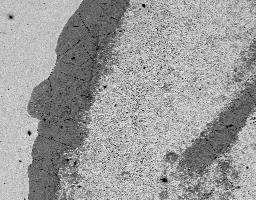
9 In-situ imaging: oxidation of steel at 800 C Formation of Cr 2 O 3 high temperatures 2 min 10 min 90 min
10 How do we get an image? Electrons out Electrons in or: x-rays out In brief: we shoot high-energy electrons and analyze the outcoming electrons/x-rays
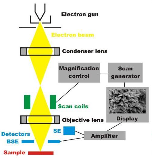
11 The instrument in brief
12 Electromagnetic Lens

13 Components of the instrument electron gun (filament) electromagnetic optics scan coils sample stage detectors vacuum system computer hardware and software (not trivial!!)
 W-wire, LaB 6 -crystal Modern: field emission guns (FEG) (cold guns, a strong electric field is used to extract electrons) Single crystal of W, etched to a thin")
14 Electron guns We want many electrons per time unit per area (high current density) and as small electron spot as possible Traditional guns: thermionic electron gun (electrons are emitted when a solid is heated) W-wire, LaB 6 -crystal Modern: field emission guns (FEG) (cold guns, a strong electric field is used to extract electrons) Single crystal of W, etched to a thin tip


15 Electron guns With field emission guns we get a smaller spot and higher current densities compared to thermionic guns Vacuum requirements are tougher for a field emission guns Single crystal of LaB 6 Tungsten wire Field emission tip
 Secondary electron detector:")
16 Detectors Backscattered electron detector: (Solid-State Detector) Secondary electron detector: (Everhart-Thornley)
17 Our traditional detectors Secondary electrons: Everhart-Thornley Detector Backscattered electrons: Solid State Diode Detector (Semiconducting device) X-rays: Energy dispersive spectrometer (EDS) (Lithium-drifted Si, Intrinsic High purity Ge)
18 Why do we need vacuum? Chemical (corrosion!!) and thermal stability is necessary for a well-functioning filament (gun pressure) A field emission gun requires ~ Torr LaB 6 : ~ 10-6 Torr The signal electrons must travel from the sample to the detector (chamber pressure) Vacuum requirements is dependant of the type of detector
19 Environmental SEM: ESEM Traditional SEM chamber pressure: ~ 10-6 Torr ESEM: Torr Various gases can be used Requires different SE detector
20 Why ESEM? To image challenging samples such as: insulating samples vacuum-sensitive samples (e.g. biological samples) irradiation-sensitive samples (e.g. thin organic films) wet samples (oily, dirty, greasy) To study and image chemical and physical processes in-situ such as: mechanical stress-testing oxidation of metals hydration/dehydration (e.g. watching paint dry)
21 Electron beam-sample interactions The incident electron beam is scattered in the sample, both elastically and inelastically This gives rise to various signals that we can detect (more on that on next slide) Interaction volume increases with increasing acceleration voltage and decreases with increasing atomic number
22 Signals from the sample Secondary electrons Backscattered electrons Incoming electrons Auger electrons X-rays Cathodoluminescence (light) Sample
23 Detection of Secondary Electron : E - T Detector

24 How do we get an image? Electron gun electrons! Detector Image
25 Where does the signals come from? Diameter of the interaction volume is larger than the electron spot resolution is poorer than the size of the electron spot
26 Secondary electrons (SE) Generated from the collision between the incoming electrons and the loosely bonded outer electrons Low energy electrons (~10-50 ev) Only SE generated close to surface escape (topographic information is obtained) Number of SE is greater than the number of incoming electrons We differentiate between SE1 and SE2
27 SE1 The secondary electrons that are generated by the incoming electron beam as they enter the surface High resolution signal with a resolution which is only limited by the electron beam diameter

28 SE2 The secondary electrons that are generated by the backscattered electrons that have returned to the surface after several inelastic scattering events SE2 come from a surface area that is bigger than the spot from the incoming electrons resolution is poorer than for SE1 exclusively Incoming electrons SE2 Sample surface
29 Factors that affect SE emission 1. Work function of the surface 2. Beam energy and beam current Electron yield goes through a maximum at low acc. voltage, then decreases with increasing acc. voltage Secondary electron yield Incident electron energy / kv
30 Factors that affect SE emission 3. Atomic number (Z) More SE2 are created with increasing Z The Z-dependence is more pronounced at lower beam energies 4. The local curvature of the surface (the most important factor)
31 Backscattered electrons (BSE) A fraction of the incident electrons is retarded by the electro-magnetic field of the nucleus and if the scattering angle is greater than 90 the electron can escape from the surface
32 Backscattered electrons (BSE) High energy electrons (elastic scattering) Fewer BSE than SE
33 Factors that affect BSE emission Direction of the irradiated surface more electrons will hit the BSE detector when the surface is aligned towards the BSE detector Average atomic number
34 BSE vs SE
35 Some comments on resolution Best resolution that can be obtained: size of the electron spot on the sample surface The introduction of FEG has dramatically improved the resolution of SEM s The volume from which the signal electrons are formed defines the resolution SE image has higher resolution than a BSE image Scanning speed: a weak signal requires slow speed to improve signalto-noise ratio when doing a slow scan drift in the electron beam can affect the accuracy of the analysis
36 Summary The scanning electron microscope is a versatile instrument that can be used for many purposes and can be equipped with various accessories An electron probe is scanned across the surface of the sample and detectors interpret the signal as a function of time A resolution of 1 2 nm can be obtained when operated in a high resolution setup The introduction of ESEM and the field emission gun have simplified the imaging of challenging samples
: mainly chemistry High energy electrons Bulk signal dependent on atomic number X-rays: chemistry Longer recording")
37 Summary Signals: Secondary electrons (SE): mainly topography Low energy electrons, high resolution Surface signal dependent on curvature Backscattered electrons (BSE): mainly chemistry High energy electrons Bulk signal dependent on atomic number X-rays: chemistry Longer recording times are needed
38 Scanning Probe Microscopy Scanning tunneling microscope Atomic force microscope

.")
 at")
39 Scanning Tunneling Microscopy Invented by Binnig and Rohrer at IBM in 1981 (Nobel Prize in Physics in 1986). Binnig also invented the Atomic Force Microscope(AFM) at Stanford University in 1986.
 images")

40 Topographic (real space) images Spectroscopic (electronic structure, density of states) images
41 Atomic resolution, several orders of magnitude better than the best electron microscope Quantum mechanical tunnel-effect of electron In-situ: capable of localized, non-destructive measurements or modifications material science, physics, semiconductor science, metallurgy, electrochemistry, and molecular biology Scanning Probe Microscopes (SPM): designed based on the scanning technology of STM
42
.")

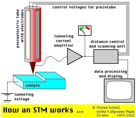
43 Tunneling Current Theory and Principle A sharp conductive tip is brought to within a few Angstroms of the surface of a conductor (sample). The surface is applied a bias voltage, Fermi levels shift The wave functions of the electrons in the tip overlap those of the sample surface Electrons tunnel from one surface to the other of lower potential.
44
45
46
47

48 Scanning Tunneling Microscopy Constant height mode Constant current mode In this mode the vertical position of the tip is not changed, equivalent to a slow or disabled feedback. The current as a function of lateral position represents the surface image. This mode is only appropriate for atomically flat surfaces as otherwise a tip crash would be inevitable. One of its advantages is that it can be used at high scanning frequencies (up to 10 khz). In comparison, the scanning frequency in the constant current mode is about 1 image per second or even per several minutes. By using a feedback loop the tip is vertically adjusted in such a way that the current always stays constant. As the current is proportional to the local density of states, the tip follows a contour of a constant density of states during scanning. A kind of a topographic image of the surface is generated by recording the vertical position of the tip.
49 Scanning tuneling spectroscopy


50 Scanning Tunneling Microscopy In case of a negative potential on the sample the occupied states generate the current, whereas in case of a positive bias the unoccupied states of the sample are of importance. Imaging the occupied states of SiC(000 )3x3 Imaging the unoccupied states of SiC(000 )3x3 By altering the voltage, a complete different image can be detected as other states contribute to the tunneling current. This is used in tunneling spectroscopy.
51
52

53 How does an AFM work?

 normal tip (3 µm tall); (b) supertip; (c)")

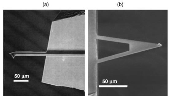
54 Invented in 1986 Cantilever Tip Surface Laser Multi-segment photodetector Figure 4. Three common types of AFM tip. (a) normal tip (3 µm tall); (b) supertip; (c) Ultralever (also 3 µm tall). Electron micrographs by Jean-Paul Revel, Caltech. Tips from Park Scientific Instruments; supertip made by Jean-Paul Revel.
55
56
57 Typical AFM Force Curves 3 2 Approach Retract Far from surface Attraction to surface surface 4 ADHESION or pull-off force 3 Cantilever bends as pushed into surface 4 Pull-off
58 3 Modes of AFM Contact Mode Non-Contact Mode Tapping (Intermittent contact) Mode
59 Contact Mode Measures repulsion between tip and sample Force of tip against sample remains constant Feedback regulation keeps cantilever deflection constant Voltage required indicates height of sample Problems: excessive tracking forces applied by probe to sample
60 Non-Contact Mode Measures attractive forces between tip and sample Tip doesn t touch sample Van der Waals forces between tip and sample detected Problems: Can t use with samples in fluid Used to analyze semiconductors Doesn t degrade or interfere with sample- better for soft samples
61

62 Tapping (Intermittent-Contact) Mode Tip vertically oscillates between contacting sample surface and lifting of at frequency of 50,000 to 500,000 cycles/sec. Oscillation amplitude reduced as probe contacts surface due to loss of energy caused by tip contacting surface Advantages: overcomes problems associated with friction, adhesion, electrostatic forces More effective for larger scan sizes
63 Tip-Surface Interaction LJ Interaction Columbic Dipolar Capillary Non Conservative forces Magnetic
64
65 Application Data storage Lithography Molecular and atomic manipulation Sensor
66
67 Introduction (cont.) Comparison between AFM and conventional ones Areal Density (Gbit/in2) Data Rate (Mbit/s) Magnetic Disk 60~ CD-ROM AFM Read: 10 Write:0.1


68 AFM Cantilevers Thermomechanical data storage systems Components: media (polymer), tip with sensors, moving scheme Digital information is represented as data pits on a polymer The sharp tip contacts with the polymer by a weak force ~0.1 un


69 Cantilevers for Writing Force + heating at tip Writing speed is limited by thermal time constant 0.34um X 51um X 40um:0.6us 1um X 100um X 16um:1us Light doping Heavy doping Bit size: 30-40nm Density: 400Gbit/in2
70
71
72
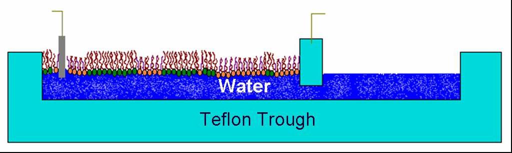
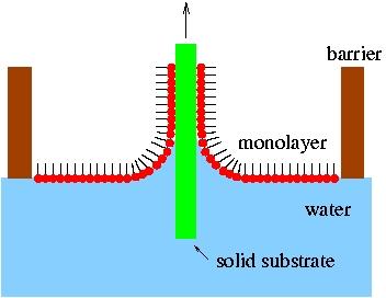
73 θ = Brewster angle for water (~ 53 o ) Source : He-Ne 30 mw polarized laser; λ = 660 nm


74 The intensity variation in the BAM images depends on: thickness of the film density of the molecule tilt and azimuth variation of the molecules
Gaetano L Episcopo. Scanning Electron Microscopy Focus Ion Beam and. Pulsed Plasma Deposition
 Gaetano L Episcopo Scanning Electron Microscopy Focus Ion Beam and Pulsed Plasma Deposition Hystorical background Scientific discoveries 1897: J. Thomson discovers the electron. 1924: L. de Broglie propose
General concept and defining characteristics of AFM. Dina Kudasheva Advisor: Prof. Mary K. Cowman
 General concept and defining characteristics of AFM Dina Kudasheva Advisor: Prof. Mary K. Cowman Overview Introduction History of the SPM invention Technical Capabilities Principles of operation Examples
Lecture 4 Scanning Probe Microscopy (SPM)
") Lecture 4 Scanning Probe Microscopy (SPM) General components of SPM; Tip --- the probe; Cantilever --- the indicator of the tip; Tip-sample interaction --- the feedback system; Scanner --- piezoelectric
Lecture 4 Scanning Probe Microscopy (SPM) General components of SPM; Tip --- the probe; Cantilever --- the indicator of the tip; Tip-sample interaction --- the feedback system; Scanner --- piezoelectric
Imaging Methods: Scanning Force Microscopy (SFM / AFM)
") Imaging Methods: Scanning Force Microscopy (SFM / AFM) The atomic force microscope (AFM) probes the surface of a sample with a sharp tip, a couple of microns long and often less than 100 Å in diameter.
Imaging Methods: Scanning Force Microscopy (SFM / AFM) The atomic force microscope (AFM) probes the surface of a sample with a sharp tip, a couple of microns long and often less than 100 Å in diameter.
Chapter 9. Electron mean free path Microscopy principles of SEM, TEM, LEEM
 Chapter 9 Electron mean free path Microscopy principles of SEM, TEM, LEEM 9.1 Electron Mean Free Path 9. Scanning Electron Microscopy (SEM) -SEM design; Secondary electron imaging; Backscattered electron
CHARACTERIZATION of NANOMATERIALS KHP
 CHARACTERIZATION of NANOMATERIALS Overview of the most common nanocharacterization techniques MAIN CHARACTERIZATION TECHNIQUES: 1.Transmission Electron Microscope (TEM) 2. Scanning Electron Microscope
MSE 321 Structural Characterization
 Auger Spectroscopy Auger Electron Spectroscopy (AES) Scanning Auger Microscopy (SAM) Incident Electron Ejected Electron Auger Electron Initial State Intermediate State Final State Physical Electronics
Scanning Probe Microscopy. Amanda MacMillan, Emmy Gebremichael, & John Shamblin Chem 243: Instrumental Analysis Dr. Robert Corn March 10, 2010
 Scanning Probe Microscopy Amanda MacMillan, Emmy Gebremichael, & John Shamblin Chem 243: Instrumental Analysis Dr. Robert Corn March 10, 2010 Scanning Probe Microscopy High-Resolution Surface Analysis
MSE 321 Structural Characterization
 Auger Spectroscopy Auger Electron Spectroscopy (AES) Scanning Auger Microscopy (SAM) Incident Electron Ejected Electron Auger Electron Initial State Intermediate State Final State Physical Electronics
HOW TO APPROACH SCANNING ELECTRON MICROSCOPY AND ENERGY DISPERSIVE SPECTROSCOPY ANALYSIS. SCSAM Short Course Amir Avishai
 HOW TO APPROACH SCANNING ELECTRON MICROSCOPY AND ENERGY DISPERSIVE SPECTROSCOPY ANALYSIS SCSAM Short Course Amir Avishai RESEARCH QUESTIONS Sea Shell Cast Iron EDS+SE Fe Cr C Objective Ability to ask the
Basic Laboratory. Materials Science and Engineering. Atomic Force Microscopy (AFM)
") Basic Laboratory Materials Science and Engineering Atomic Force Microscopy (AFM) M108 Stand: 20.10.2015 Aim: Presentation of an application of the AFM for studying surface morphology. Inhalt 1.Introduction...
Basic Laboratory Materials Science and Engineering Atomic Force Microscopy (AFM) M108 Stand: 20.10.2015 Aim: Presentation of an application of the AFM for studying surface morphology. Inhalt 1.Introduction...
= 6 (1/ nm) So what is probability of finding electron tunneled into a barrier 3 ev high?
 So what is probability of finding electron tunneled into a barrier 3 ev high?") STM STM With a scanning tunneling microscope, images of surfaces with atomic resolution can be readily obtained. An STM uses quantum tunneling of electrons to map the density of electrons on the surface
STM STM With a scanning tunneling microscope, images of surfaces with atomic resolution can be readily obtained. An STM uses quantum tunneling of electrons to map the density of electrons on the surface
Contents. What is AFM? History Basic principles and devices Operating modes Application areas Advantages and disadvantages
 Contents What is AFM? History Basic principles and devices Operating modes Application areas Advantages and disadvantages Figure1: 2004 Seth Copen Goldstein What is AFM? A type of Scanning Probe Microscopy
SCANNING ELECTRON MICROSCOPE
 21.05.2010 Hacettepe University SCANNING ELECTRON MICROSCOPE Berrak BOYBEK Tuğba ÖZTÜRK Vicdan PINARBAŞI Cahit YAYAN OUTLINE Definition of scanning electron microscope History Applications of SEM Components
Ecole Franco-Roumaine : Magnétisme des systèmes nanoscopiques et structures hybrides - Brasov, Modern Analytical Microscopic Tools
 1. Introduction Solid Surfaces Analysis Group, Institute of Physics, Chemnitz University of Technology, Germany 2. Limitations of Conventional Optical Microscopy 3. Electron Microscopies Transmission Electron
Scanning Tunneling Microscopy
 Scanning Tunneling Microscopy References: 1. G. Binnig, H. Rohrer, C. Gerber, and Weibel, Phys. Rev. Lett. 49, 57 (1982); and ibid 50, 120 (1983). 2. J. Chen, Introduction to Scanning Tunneling Microscopy,
Basic structure of SEM
 Table of contents Basis structure of SEM SEM imaging modes Comparison of ordinary SEM and FESEM Electron behavior Electron matter interaction o Elastic interaction o Inelastic interaction o Interaction
Scanning Electron Microscopy
 Scanning Electron Microscopy Field emitting tip Grid 2kV 100kV Anode ZEISS SUPRA Variable Pressure FESEM Dr Heath Bagshaw CMA bagshawh@tcd.ie Why use an SEM? Fig 1. Examples of features resolvable using
Electron Microprobe Analysis 1 Nilanjan Chatterjee, Ph.D. Principal Research Scientist
 12.141 Electron Microprobe Analysis 1 Nilanjan Chatterjee, Ph.D. Principal Research Scientist Massachusetts Institute of Technology Electron Microprobe Facility Department of Earth, Atmospheric and Planetary
MS482 Materials Characterization ( 재료분석 ) Lecture Note 11: Scanning Probe Microscopy. Byungha Shin Dept. of MSE, KAIST
 Lecture Note 11: Scanning Probe Microscopy. Byungha Shin Dept. of MSE, KAIST") 2015 Fall Semester MS482 Materials Characterization ( 재료분석 ) Lecture Note 11: Scanning Probe Microscopy Byungha Shin Dept. of MSE, KAIST 1 Course Information Syllabus 1. Overview of various characterization
2015 Fall Semester MS482 Materials Characterization ( 재료분석 ) Lecture Note 11: Scanning Probe Microscopy Byungha Shin Dept. of MSE, KAIST 1 Course Information Syllabus 1. Overview of various characterization
Characterization of MEMS Devices
 MEMS: Characterization Characterization of MEMS Devices Prasanna S. Gandhi Assistant Professor, Department of Mechanical Engineering, Indian Institute of Technology, Bombay, Recap Characterization of MEMS
Chapter 10. Nanometrology. Oxford University Press All rights reserved.
 Chapter 10 Nanometrology Oxford University Press 2013. All rights reserved. 1 Introduction Nanometrology is the science of measurement at the nanoscale level. Figure illustrates where nanoscale stands
Electron Microprobe Analysis 1 Nilanjan Chatterjee, Ph.D. Principal Research Scientist
 12.141 Electron Microprobe Analysis 1 Nilanjan Chatterjee, Ph.D. Principal Research Scientist Massachusetts Institute of Technology Electron Microprobe Facility Department of Earth, Atmospheric and Planetary
Instrumentation and Operation
 Instrumentation and Operation 1 STM Instrumentation COMPONENTS sharp metal tip scanning system and control electronics feedback electronics (keeps tunneling current constant) image processing system data
Module 26: Atomic Force Microscopy. Lecture 40: Atomic Force Microscopy 3: Additional Modes of AFM
 Module 26: Atomic Force Microscopy Lecture 40: Atomic Force Microscopy 3: Additional Modes of AFM 1 The AFM apart from generating the information about the topography of the sample features can be used
Part II: Thin Film Characterization
 Part II: Thin Film Characterization General details of thin film characterization instruments 1. Introduction to Thin Film Characterization Techniques 2. Structural characterization: SEM, TEM, AFM, STM
Program Operacyjny Kapitał Ludzki SCANNING PROBE TECHNIQUES - INTRODUCTION
 Program Operacyjny Kapitał Ludzki SCANNING PROBE TECHNIQUES - INTRODUCTION Peter Liljeroth Department of Applied Physics, Aalto University School of Science peter.liljeroth@aalto.fi Projekt współfinansowany
Techniken der Oberflächenphysik (Techniques of Surface Physics)
") Techniken der Oberflächenphysik (Techniques of Surface Physics) Prof. Yong Lei & Dr. Yang Xu Fachgebiet 3D-Nanostrukturierung, Institut für Physik Contact: yong.lei@tu-ilmenau.de yang.xu@tu-ilmenau.de
Techniken der Oberflächenphysik (Techniques of Surface Physics) Prof. Yong Lei & Dr. Yang Xu Fachgebiet 3D-Nanostrukturierung, Institut für Physik Contact: yong.lei@tu-ilmenau.de yang.xu@tu-ilmenau.de
STM: Scanning Tunneling Microscope
 STM: Scanning Tunneling Microscope Basic idea STM working principle Schematic representation of the sample-tip tunnel barrier Assume tip and sample described by two infinite plate electrodes Φ t +Φ s =
Electron beam scanning
 Electron beam scanning The Electron beam scanning operates through an electro-optical system which has the task of deflecting the beam Synchronously with cathode ray tube which create the image, beam moves
Everhart-Thornley detector
 SEI Detector Everhart-Thornley detector Microscope chamber wall Faraday cage Scintillator Electrons in Light pipe Photomultiplier Electrical signal out Screen Quartz window +200 V +10 kv Always contains
Quantum Condensed Matter Physics Lecture 12
 Quantum Condensed Matter Physics Lecture 12 David Ritchie QCMP Lent/Easter 2016 http://www.sp.phy.cam.ac.uk/drp2/home 12.1 QCMP Course Contents 1. Classical models for electrons in solids 2. Sommerfeld
Scanning Probe Microscopy. EMSE-515 F. Ernst
 Scanning Probe Microscopy EMSE-515 F. Ernst 1 Literature 2 3 Scanning Probe Microscopy: The Lab on a Tip by Ernst Meyer,Ans Josef Hug,Roland Bennewitz 4 Scanning Probe Microscopy and Spectroscopy : Theory,
Chapter 12. Nanometrology. Oxford University Press All rights reserved.
 Chapter 12 Nanometrology Introduction Nanometrology is the science of measurement at the nanoscale level. Figure illustrates where nanoscale stands in relation to a meter and sub divisions of meter. Nanometrology
Atomic and molecular interactions. Scanning probe microscopy.
 Atomic and molecular interactions. Scanning probe microscopy. Balázs Kiss Nanobiotechnology and Single Molecule Research Group, Department of Biophysics and Radiation Biology 27. November 2013. 2 Atomic
Experimental methods in physics. Local probe microscopies I
 Experimental methods in physics Local probe microscopies I Scanning tunnelling microscopy (STM) Jean-Marc Bonard Academic year 09-10 1. Scanning Tunneling Microscopy 1.1. Introduction Image of surface
Scanning Tunneling Microscopy
 Scanning Tunneling Microscopy Scanning Direction References: Classical Tunneling Quantum Mechanics Tunneling current Tunneling current I t I t (V/d)exp(-Aφ 1/2 d) A = 1.025 (ev) -1/2 Å -1 I t = 10 pa~10na
Nova 600 NanoLab Dual beam Focused Ion Beam IITKanpur
 Nova 600 NanoLab Dual beam Focused Ion Beam system @ IITKanpur Dual Beam Nova 600 Nano Lab From FEI company (Dual Beam = SEM + FIB) SEM: The Electron Beam for SEM Field Emission Electron Gun Energy : 500
Scanning Probe Microscopy (SPM)
") CHEM53200: Lecture 9 Scanning Probe Microscopy (SPM) Major reference: 1. Scanning Probe Microscopy and Spectroscopy Edited by D. Bonnell (2001). 2. A practical guide to scanning probe microscopy by Park
CHEM53200: Lecture 9 Scanning Probe Microscopy (SPM) Major reference: 1. Scanning Probe Microscopy and Spectroscopy Edited by D. Bonnell (2001). 2. A practical guide to scanning probe microscopy by Park
MEMS Metrology. Prof. Tianhong Cui ME 8254
 MEMS Metrology Prof. Tianhong Cui ME 8254 What is metrology? Metrology It is the science of weights and measures Refers primarily to the measurements of length, weight, time, etc. Mensuration- A branch
Outline Scanning Probe Microscope (SPM)
") AFM Outline Scanning Probe Microscope (SPM) A family of microscopy forms where a sharp probe is scanned across a surface and some tip/sample interactions are monitored Scanning Tunneling Microscopy (STM)
AFM Outline Scanning Probe Microscope (SPM) A family of microscopy forms where a sharp probe is scanned across a surface and some tip/sample interactions are monitored Scanning Tunneling Microscopy (STM)
Introduction to Scanning Probe Microscopy Zhe Fei
 Introduction to Scanning Probe Microscopy Zhe Fei Phys 590B, Apr. 2019 1 Outline Part 1 SPM Overview Part 2 Scanning tunneling microscopy Part 3 Atomic force microscopy Part 4 Electric & Magnetic force
INDIAN INSTITUTE OF TECHNOLOGY ROORKEE NPTEL NPTEL ONLINE CERTIFICATION COURSE. Biomedical Nanotechnology. Lec-05 Characterisation of Nanoparticles
 INDIAN INSTITUTE OF TECHNOLOGY ROORKEE NPTEL NPTEL ONLINE CERTIFICATION COURSE Biomedical Nanotechnology Lec-05 Characterisation of Nanoparticles Dr. P. Gopinath Department of Biotechnology Indian Institute
Scanning Tunneling Microscopy Transmission Electron Microscopy
 Scanning Tunneling Microscopy Transmission Electron Microscopy Speakers Burcu Başar Semih Gezgin Yavuz Selim Telis Place Hacettepe University Department of Chemical Engineering It s a small world after
Scanning Force Microscopy II
 Scanning Force Microscopy II Measurement modes Magnetic force microscopy Artifacts Lars Johansson 1 SFM - Forces Chemical forces (short range) Van der Waals forces Electrostatic forces (long range) Capillary
h p λ = mν Back to de Broglie and the electron as a wave you will learn more about this Equation in CHEM* 2060
 Back to de Broglie and the electron as a wave λ = mν h = h p you will learn more about this Equation in CHEM* 2060 We will soon see that the energies (speed for now if you like) of the electrons in the
AP5301/ Name the major parts of an optical microscope and state their functions.
 Review Problems on Optical Microscopy AP5301/8301-2015 1. Name the major parts of an optical microscope and state their functions. 2. Compare the focal lengths of two glass converging lenses, one with
tip of a current tip and the sample. Components: 3. Coarse sample-to-tip isolation system, and
 SCANNING TUNNELING MICROSCOPE Brief history: Heinrich Rohrer and Gerd K. Binnig, scientists at IBM's Zurich Research Laboratory in Switzerland, are awarded the 1986 Nobel Prize in physicss for their work
Nanostructure. Materials Growth Characterization Fabrication. More see Waser, chapter 2
 Nanostructure Materials Growth Characterization Fabrication More see Waser, chapter 2 Materials growth - deposition deposition gas solid Physical Vapor Deposition Chemical Vapor Deposition Physical Vapor
Scanning Force Microscopy
 Scanning Force Microscopy Roland Bennewitz Rutherford Physics Building 405 Phone 398-3058 roland.bennewitz@mcgill.ca Scanning Probe is moved along scan lines over a sample surface 1 Force Microscopy Data
Characterization Tools
 Lectures in Nanoscience & Technology Characterization Tools K. Sakkaravarthi Department of Physics National Institute of Technology Tiruchirappalli 620 015 Tamil Nadu India sakkaravarthi@nitt.edu ksakkaravarthi.weebly.com
Why microscopy?
 Electron Microscopy Why microscopy? http://www.cellsalive.com/howbig.htm 2 Microscopes are used as magnifying tools (although not exclusively as will see later on). The resolution of the human eye is limited
Scanning Tunneling Microscopy Studies of the Ge(111) Surface
 Surface") VC Scanning Tunneling Microscopy Studies of the Ge(111) Surface Anna Rosen University of California, Berkeley Advisor: Dr. Shirley Chiang University of California, Davis August 24, 2007 Abstract: This
VC Scanning Tunneling Microscopy Studies of the Ge(111) Surface Anna Rosen University of California, Berkeley Advisor: Dr. Shirley Chiang University of California, Davis August 24, 2007 Abstract: This
NIS: what can it be used for?
 AFM @ NIS: what can it be used for? Chiara Manfredotti 011 670 8382/8388/7879 chiara.manfredotti@to.infn.it Skype: khiaram 1 AFM: block scheme In an Atomic Force Microscope (AFM) a micrometric tip attached
ABC s of Electrochemistry series Materials Characterization techniques: SEM and EDS Ana María Valenzuela-Muñiz November 3, 2011
 ABC s of Electrochemistry series Materials Characterization techniques: SEM and EDS Ana María Valenzuela-Muñiz November 3, 2011 CEER, Department of Chemical and Biomolecular Engineering Outline Introduction
Kavli Workshop for Journalists. June 13th, CNF Cleanroom Activities
 Kavli Workshop for Journalists June 13th, 2007 CNF Cleanroom Activities Seeing nm-sized Objects with an SEM Lab experience: Scanning Electron Microscopy Equipment: Zeiss Supra 55VP Scanning electron microscopes
From nanophysics research labs to cell phones. Dr. András Halbritter Department of Physics associate professor
 From nanophysics research labs to cell phones Dr. András Halbritter Department of Physics associate professor Curriculum Vitae Birth: 1976. High-school graduation: 1994. Master degree: 1999. PhD: 2003.
PHI 5000 Versaprobe-II Focus X-ray Photo-electron Spectroscopy
 PHI 5000 Versaprobe-II Focus X-ray Photo-electron Spectroscopy The very basic theory of XPS XPS theroy Surface Analysis Ultra High Vacuum (UHV) XPS Theory XPS = X-ray Photo-electron Spectroscopy X-ray
Modern Optical Spectroscopy
 Modern Optical Spectroscopy X-Ray Microanalysis Shu-Ping Lin, Ph.D. Institute of Biomedical Engineering E-mail: splin@dragon.nchu.edu.tw Website: http://web.nchu.edu.tw/pweb/users/splin/ Backscattered
SEM Optics and Application to Current Research
 SEM Optics and Application to Current Research Azure Avery May 28, 2008 1 Introduction 1.1 History The optical microscope was invented in the early 17th century. Although revolutionary, the earliest microscopes
Massachusetts Institute of Technology. Dr. Nilanjan Chatterjee
 Massachusetts Institute of Technology Dr. Nilanjan Chatterjee Electron Probe Micro-Analysis (EPMA) Imaging and micrometer-scale chemical compositional analysis of solids Signals produced in The Electron
Electron Microprobe Analysis and Scanning Electron Microscopy
 Electron Microprobe Analysis and Scanning Electron Microscopy Electron microprobe analysis (EMPA) Analytical technique in which a beam of electrons is focused on a sample surface, producing X-rays from
Scanning Tunneling Microscopy
 Scanning Tunneling Microscopy A scanning tunneling microscope (STM) is an instrument for imaging surfaces at the atomic level. Its development in 1981 earned its inventors, Gerd Binnig and Heinrich Rohrer
And Manipulation by Scanning Probe Microscope
 Basic 15 Nanometer Scale Measurement And Manipulation by Scanning Probe Microscope Prof. K. Fukuzawa Dept. of Micro/Nano Systems Engineering Nagoya University I. Basics of scanning probe microscope Basic
MSN551 LITHOGRAPHY II
 MSN551 Introduction to Micro and Nano Fabrication LITHOGRAPHY II E-Beam, Focused Ion Beam and Soft Lithography Why need electron beam lithography? Smaller features are required By electronics industry:
Atomic Force Microscopy imaging and beyond
 Atomic Force Microscopy imaging and beyond Arif Mumtaz Magnetism and Magnetic Materials Group Department of Physics, QAU Coworkers: Prof. Dr. S.K.Hasanain M. Tariq Khan Alam Imaging and beyond Scanning
Nitride HFETs applications: Conductance DLTS
 Nitride HFETs applications: Conductance DLTS The capacitance DLTS cannot be used for device trap profiling as the capacitance for the gate will be very small Conductance DLTS is similar to capacitance
Scanning Probe Microscopy (SPM)
") Scanning Probe Microscopy (SPM) Scanning Tunneling Microscopy (STM) --- G. Binnig, H. Rohrer et al, (1982) Near-Field Scanning Optical Microscopy (NSOM) --- D. W. Pohl (1982) Atomic Force Microscopy (AFM)
Scanning Probe Microscopy (SPM) Scanning Tunneling Microscopy (STM) --- G. Binnig, H. Rohrer et al, (1982) Near-Field Scanning Optical Microscopy (NSOM) --- D. W. Pohl (1982) Atomic Force Microscopy (AFM)
MT Electron microscopy Scanning electron microscopy and electron probe microanalysis
 MT-0.6026 Electron microscopy Scanning electron microscopy and electron probe microanalysis Eero Haimi Research Manager Outline 1. Introduction Basics of scanning electron microscopy (SEM) and electron
Transmission Electron Microscopy
 L. Reimer H. Kohl Transmission Electron Microscopy Physics of Image Formation Fifth Edition el Springer Contents 1 Introduction... 1 1.1 Transmission Electron Microscopy... 1 1.1.1 Conventional Transmission
Auger Electron Spectroscopy
 Auger Electron Spectroscopy Auger Electron Spectroscopy is an analytical technique that provides compositional information on the top few monolayers of material. Detect all elements above He Detection
Lecture 26 MNS 102: Techniques for Materials and Nano Sciences
 Lecture 26 MNS 102: Techniques for Materials and Nano Sciences Reference: #1 C. R. Brundle, C. A. Evans, S. Wilson, "Encyclopedia of Materials Characterization", Butterworth-Heinemann, Toronto (1992),
Scanning Probe Microscopy
 1 Scanning Probe Microscopy Dr. Benjamin Dwir Laboratory of Physics of Nanostructures (LPN) Benjamin.dwir@epfl.ch PH.D3.344 Outline: Introduction: What is SPM, history STM AFM Image treatment Advanced
Intermittent-Contact Mode Force Microscopy & Electrostatic Force Microscopy (EFM)
") WORKSHOP Nanoscience on the Tip Intermittent-Contact Mode Force Microscopy & Electrostatic Force Microscopy (EFM) Table of Contents: 1. Motivation... 1. Simple Harmonic Motion... 1 3. AC-Mode Imaging...
WORKSHOP Nanoscience on the Tip Intermittent-Contact Mode Force Microscopy & Electrostatic Force Microscopy (EFM) Table of Contents: 1. Motivation... 1. Simple Harmonic Motion... 1 3. AC-Mode Imaging...
Characterization of MEMS Devices
 MEMS: Characterization Characterization of MEMS Devices Prasanna S. Gandhi Assistant Professor, Department of Mechanical Engineering, Indian Institute of Technology, Bombay, Recap Fabrication of MEMS Conventional
Scanning Electron Microscopy
 Scanning Electron Microscopy Amanpreet Kaur 1 www.reading.ac.uk/emlab Scanning Electron Microscopy What is scanning electron microscopy? Basic features of conventional SEM Limitations of conventional SEM
Nanoelectronics 09. Atsufumi Hirohata Department of Electronics. Quick Review over the Last Lecture
 Nanoelectronics 09 Atsufumi Hirohata Department of Electronics 13:00 Monday, 12/February/2018 (P/T 006) Quick Review over the Last Lecture ( Field effect transistor (FET) ): ( Drain ) current increases
Characterisation of Catalysts Using Secondary and Backscattered Electron In-lens Detectors
 Platinum Metals Rev., 2014, 58, (2), 106 110 FINAL ANALYSIS Characterisation of Catalysts Using Secondary and Backscattered Electron In-lens Detectors Heterogeneous catalysis often involves the use of
Introduction to Electron Beam Lithography
 Introduction to Electron Beam Lithography Boštjan Berčič (bostjan.bercic@ijs.si), Jožef Štefan Institute, Jamova 39, 1000 Ljubljana, Slovenia 1. Introduction Electron Beam Lithography is a specialized
Scanning Tunneling Microscopy
 Scanning Tunneling Microscopy References: 1. G. Binnig, H. Rohrer, C. Gerber, and Weibel, Phys. Rev. Lett. 49, 57 (1982); and ibid 50, 120 (1983). 2. J. Chen, Introduction to Scanning Tunneling Microscopy,
Chapter 4. Characterization
 Chapter 4. Characterization Tools for Characterization Structural analysis: SEM, TEM, XRD, SAM, SPM, PEEM, LEEM, STXM, SXPEM Chemical analysis: AES, XPS, TPD, SIMS, EDX, SPM Electronic, optical analysis:
MSE 321 Structural Characterization
 Optical Microscope Plan Lenses In an "ideal" single-element lens system all planar wave fronts are focused to a point at distance f from the lens; therefore: Image near the optical axis will be in perfect
Lecture 12: Biomaterials Characterization in Aqueous Environments
 3.051J/20.340J 1 Lecture 12: Biomaterials Characterization in Aqueous Environments High vacuum techniques are important tools for characterizing surface composition, but do not yield information on surface
MAGNETIC FORCE MICROSCOPY
 University of Ljubljana Faculty of Mathematics and Physics Department of Physics SEMINAR MAGNETIC FORCE MICROSCOPY Author: Blaž Zupančič Supervisor: dr. Igor Muševič February 2003 Contents 1 Abstract 3
The illumination source: the electron beam
 The SEM Column The illumination source: the electron beam The probe of the electron microscope is an electron beam with very high and stable energy (10-100 kev) in order to get images with high resolution.
MT Electron microscopy Scanning electron microscopy and electron probe microanalysis
 MT-0.6026 Electron microscopy Scanning electron microscopy and electron probe microanalysis Eero Haimi Research Manager Outline 1. Introduction Basics of scanning electron microscopy (SEM) and electron
From Last Time. Mon. Nov 8 Phy107 Lecture 26
 From Last Time Particle can exist in different quantum states, having Different energy Different momentum Different wavelength The quantum wavefunction describes wave nature of particle. Square of the
Microscopie a stilo: principi ed esempi di applicazione
 Microscopie a stilo: principi ed esempi di applicazione Adele Sassella Dipartimento di Scienza dei Materiali Università degli Studi di Milano Bicocca adele.sassella@unimib.it Pavia, 22 aprile 2009 SCANNING
Auger Electron Spectroscopy Overview
 Auger Electron Spectroscopy Overview Also known as: AES, Auger, SAM 1 Auger Electron Spectroscopy E KLL = E K - E L - E L AES Spectra of Cu EdN(E)/dE Auger Electron E N(E) x 5 E KLL Cu MNN Cu LMM E f E
Instability & Pattering of Thin Polymer Films Prof. R. Mukherjee Department of Chemical Engineering Indian Institute of Technology Kharagpur
 Instability & Pattering of Thin Polymer Films Prof. R. Mukherjee Department of Chemical Engineering Indian Institute of Technology Kharagpur Lecture No#26 Atomic Force Microscope V (Refer Slide Time: 00:34)
Sensors and Metrology. Outline
 Sensors and Metrology A Survey 1 Outline General Issues & the SIA Roadmap Post-Process Sensing (SEM/AFM, placement) In-Process (or potential in-process) Sensors temperature (pyrometry, thermocouples, acoustic
Practical course in scanning electron microscopy
 Practical course in scanning electron microscopy Fortgeschrittenen Praktikum an der Technischen Universität München Wintersemester 2017/2018 Table of contents 1. Introduction 3 2. Formation of an electron
Auger Electron Spectroscopy (AES)
") 1. Introduction Auger Electron Spectroscopy (AES) Silvia Natividad, Gabriel Gonzalez and Arena Holguin Auger Electron Spectroscopy (Auger spectroscopy or AES) was developed in the late 1960's, deriving
1. Introduction Auger Electron Spectroscopy (AES) Silvia Natividad, Gabriel Gonzalez and Arena Holguin Auger Electron Spectroscopy (Auger spectroscopy or AES) was developed in the late 1960's, deriving
672 Advanced Solid State Physics. Scanning Tunneling Microscopy
 672 Advanced Solid State Physics Scanning Tunneling Microscopy Biao Hu Outline: 1. Introduction to STM 2. STM principle & working modes 3. STM application & extension 4. STM in our group 1. Introduction
INTRODUCTION TO SCA\ \I\G TUNNELING MICROSCOPY
 INTRODUCTION TO SCA\ \I\G TUNNELING MICROSCOPY SECOND EDITION C. JULIAN CHEN Department of Applied Physics and Applied Mathematics, Columbia University, New York OXFORD UNIVERSITY PRESS Contents Preface
CBE Science of Engineering Materials. Scanning Electron Microscopy (SEM)
") CBE 30361 Science of Engineering Materials Scanning Electron Microscopy (SEM) Scale of Structure Organization Units: micrometer = 10-6 m = 1µm nanometer= 10-9 m = 1nm Angstrom = 10-10 m = 1Å A hair is
CBE 30361 Science of Engineering Materials Scanning Electron Microscopy (SEM) Scale of Structure Organization Units: micrometer = 10-6 m = 1µm nanometer= 10-9 m = 1nm Angstrom = 10-10 m = 1Å A hair is
An Introduction to Auger Electron Spectroscopy
 An Introduction to Auger Electron Spectroscopy Spyros Diplas MENA3100 SINTEF Materials & Chemistry, Department of Materials Physics & Centre of Materials Science and Nanotechnology, Department of Chemistry,
Università degli Studi di Bari "Aldo Moro"
 Università degli Studi di Bari "Aldo Moro" Table of contents 1. Introduction to Atomic Force Microscopy; 2. Introduction to Raman Spectroscopy; 3. The need for a hybrid technique Raman AFM microscopy;
SCANNING-PROBE TECHNIQUES OR APPARATUS; APPLICATIONS OF SCANNING-PROBE TECHNIQUES, e.g. SCANNING PROBE MICROSCOPY [SPM]
![SCANNING-PROBE TECHNIQUES OR APPARATUS; APPLICATIONS OF SCANNING-PROBE TECHNIQUES, e.g. SCANNING PROBE MICROSCOPY [SPM]](/thumbs/81/83165631.jpg "SCANNING-PROBE TECHNIQUES OR APPARATUS; APPLICATIONS OF SCANNING-PROBE TECHNIQUES, e.g. SCANNING PROBE MICROSCOPY [SPM]") G01Q SCANNING-PROBE TECHNIQUES OR APPARATUS; APPLICATIONS OF SCANNING-PROBE TECHNIQUES, e.g. SCANNING PROBE MICROSCOPY [SPM] Scanning probes, i.e. devices having at least a tip of nanometre sized dimensions
G01Q SCANNING-PROBE TECHNIQUES OR APPARATUS; APPLICATIONS OF SCANNING-PROBE TECHNIQUES, e.g. SCANNING PROBE MICROSCOPY [SPM] Scanning probes, i.e. devices having at least a tip of nanometre sized dimensions
Scanning Tunneling Microscopy
 Scanning Tunneling Microscopy References: 1. G. Binnig, H. Rohrer, C. Gerber, and Weibel, Phys. Rev. Lett. 49, 57 (1982); and ibid 50, 120 (1983). 2. J. Chen, Introduction to Scanning Tunneling Microscopy,