HOW TO APPROACH SCANNING ELECTRON MICROSCOPY AND ENERGY DISPERSIVE SPECTROSCOPY ANALYSIS. SCSAM Short Course Amir Avishai
|
|
|
- Rafe Kelley
- 6 years ago
- Views:
Transcription
1 HOW TO APPROACH SCANNING ELECTRON MICROSCOPY AND ENERGY DISPERSIVE SPECTROSCOPY ANALYSIS SCSAM Short Course Amir Avishai
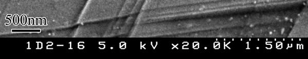
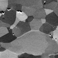
2 RESEARCH QUESTIONS Sea Shell Cast Iron EDS+SE Fe Cr C Objective Ability to ask the right questions! 50nm Cu Vias First Order Lamellar Interface Image showing detail of axons and myelin sheaths, Mitochondria.
3 CHARACTERIZATION IS PART OF THE EXPERIMENT! SE 30kV BSE 30kV SE 6kV BSE 6kV Amir Avishai


4 POKE AND LISTEN Dr. Wayne Jennings Source/Beam/Probe Interaction/Signal Detector Data Interpretation / Contrast mechanisms


5 LIGHT VS SEM / TEM Based on Abbe s theory you cannot resolve structure below about ½ the wavelength of the probe. Electron beam 54pm (500 ev) Electron beam 2pm (300 KeV) 78% of speed of light Visible light nm wavelength Resolution Notes: 1nm=1000pm, typical atomic spacing 0.1nm
6 OUTLINE - Beam optics and image formation. - Signals Generated in an SEM and their detection. - Beam energy & current. - EDS - compositional analysis. - What else can we do with an SEM? - How do we approach a new sample?


7 BASIC OPERATION MODE OF SEM Schematic diagram illustrating the essential components of an SEM. Note that an array of useful signals can be collected and analyzed by use of different detectors.


8 IMAGE FORMATION IN SEM One pixel at a time! Very small beam convergence angle Large depth of field Ratio of the area viewed to the area being scanned is magnification


9 CORALS VERY LARGE DEPTH OF FIELD light microscope /2 rad (1.57 rad) Electron microscope 10-3 rad 9 Effective Focus Amir Avishai
10 OUTLINE - Beam optics and image formation. - Signals Generated in an SEM and their detection. - Beam energy & current. - EDS - compositional analysis. - What else can we do with an SEM? - How do we approach a new sample?

11 WHAT TYPE SIGNALS ARE CREATED IN A SEM? Backscattered electron diffraction Crystal structure - phase

12 DETECTORS AVAILABLE Everhart Thornley (ETD) Detector (SE, BSE) InLens(TLD) Detector SE, BSE Detection ICE Detector (SE, BSE, ions) Retractable STEM Detector (BF, DF, HAADF) Retractable Solid state BSE Detector GSED SE Detection EDS Photon Detection and Energy Analysis EBSD Backscattered Electron Diffraction Beam Deceleration EDS Detector TLD Detector
 BSE (kev) III SE (ev) N(E/E 0 ) E/E 0 SEs are VERY low energy electrons! By definition, these secondary electrons are <50 ev, with most 3-5 ev.")
13 CHARACTERISTICS OF SECONDARY AND BSE ELECTRONS Energy distribution of all electrons emitted from specimen under kev electron bombardment: SE: Topographic BSE: Compositional SE (ev) BSE (kev) III SE (ev) N(E/E 0 ) E/E 0 SEs are VERY low energy electrons! By definition, these secondary electrons are <50 ev, with most 3-5 ev. Millipede - FEI
 ~ elastic")
14 ELECTRON BEAM PENETRATION SE Few nm BSE Electron Excited X-Rays m MONTE CARLO 1 m - Beam penetration decreases with Z - Beam penetration increases with energy - Electron range ~ inelastic processes - Electron scattering (aspect) ~ elastic processes

15 SURFACE IMAGING TOPOGRAPHY, CRYSTAL SYMMETRY Zero Tilt Tilt and kv Tilt Angle Beam Energy High Tilt SE properties Amir Avishai

![Amir Avishai Si [at%] Mo [at%] O [at%] Other 1](/docs-images/73/68395368/images/16-3.jpg "25 46.5 28.5 2 54 31 15 16 3 28.5 0.")
16 BACKSCATTER ELECTRON PRODUCTION Mo, Si, O BSE Yield SE Yield keV Z- Atomic number Amir Avishai Si [at%] Mo [at%] O [at%] Other (Al,Mg Ca)

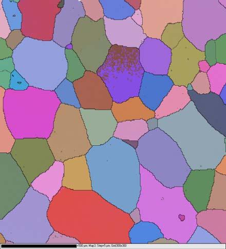
17 Electron Back Scattered Diffraction Patterns (EBSD) Orientation Imaging Mapping (OIM) Oxford Instruments 500 μm 17


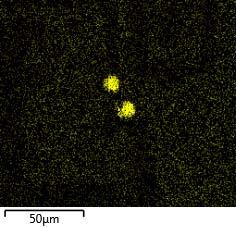
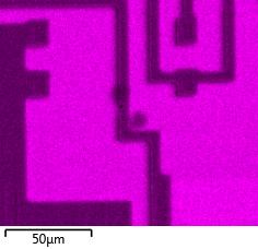
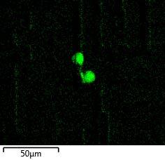
18 DETECTOR POSITION & CONTRAST SE Image Deweting of Ni Film over Sapphire Where is the detector? Scintillator ETD Grid Amir Avishai
19 OUTLINE - Beam optics and image formation. - Signals Generated in an SEM and their detection. - Beam energy & current. - EDS - compositional analysis. - What else can we do with an SEM? - How do we approach a new sample?
20 BSE VS SE AND VOLTAGE SE 30kV BSE 30kV Effects seen here are a result of variation in two parameters only! SE 6kV BSE 6kV Amir Avishai

21 BEAM ENERGY AND PENETRATION x50 x200 5 kv 25 kv


22 BIOLOGICAL TISSUE IMAGING Moth Sensors Critical point dried Rods in a Wild Mouse Eye Debarshi Mustafi CWRU, SOM Mark Willis, CWRU, Biology To obtain BSE contrast samples are stained with heavy metals Osmium, Uranium, lead and Fe. Brain Tissue Grahame Kidd CCF
23 OUTLINE - Beam optics and image formation. - Signals Generated in an SEM and their detection. - Beam energy & current. - EDS - compositional analysis. - What else can we do with an SEM? - How do we approach a new sample?
24 COMPOSITIONAL INFORMATION ENERGY DISPERSIVE SPECTROSCOPY (EDS) X-ray Lines - K, L, M Nomenclature for Principal X Ray Emission Lines 24
 R x [ m] E 0 - [KeV] E C - [KeV] g/cm 3 F A depth-distribution function, φ(ρz), 3g/cm3 Cu in Al 20kV 8g/cm3 Al in")
25 X-RAY GENERATION VOLUME Atomic number correction (Z) Absorption correction (A) Characteristic fluorescence correction (F). (. -. ) R x [ m] E 0 - [KeV] E C - [KeV] g/cm 3 F A depth-distribution function, φ(ρz), 3g/cm3 Cu in Al 20kV 8g/cm3 Al in Cu
. - Measure on a uniform region.")


26 REQUIRED CONDITIONS FOR EDS ANALYSIS - Polished sample (flat). - Measure on a uniform region. - No etching, use BSE to identify phases. - Use a beam energy 2-3 times the highest peak analyzed. - For charging samples avoid metallic coatings if possible, use carbon. - Repeat measurement in a few locations
27 IDENTIFYING ELEMENTS & OVERLAPPING PEAKS - Never trust auto ID, confirm every peak. - In case of severe overlaps use higher energies to confirm elements. - Use longer processing time to better resolve peaks or long collection times (better statistics). Oxford Instruments


28 WORKING WITH EDS MAPPING Naima Hilli CWRU, DMSE


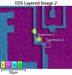
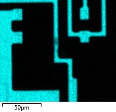
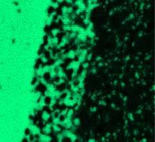
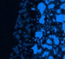
29 Failure Analysis - Device Si Al Si C N O Al P P O


30 COMMON ARTIFACTS & ERRORS DURING ANALYSIS Sum/pileup Peaks Si X-Ray Escape peaks Errors due to charging (Duane-Hunt limit). Background removal in elemental maps. Working distance Magnification.
31 OUTLINE - Beam optics and image formation. - Signals Generated in an SEM and their detection. - Beam energy & current. - EDS - compositional analysis. - What else can we do with an SEM? - How do we approach a new sample?
32 VPSEM CAPABILITIES Conventional High Vacuum Coated/conductive specimens Critical point dried specimens Low Vacuum or Wet Mode Charge reduction for non conductors Surface imaging in a gas (hydration/dehydration, oxidation studies) Vacuum sensitive materials (biological samples) Wet or dirty specimens (ESEM) I. Working Distance II. III. Gas Pressure Accelerating Voltage


33 HIGH TEMPERATURE HYDRATION- LILY POLLEN Images compliments of FEI 33
 IN")

34 FRESH LACCARIA (TREE FUNGUS) IN AN ESEM Images compliments of FEI


35 STEM IN SEM: MULTIPLE SIGNALS COLLECTED SIMULTANEOUSLY Mark DeGuire CWRU Pt Pd CdS F SnO 2 Glass BF DF HAADF The user has not direct control over the camera length
36 OUTLINE - Beam optics and image formation. - Signals Generated in an SEM and their detection. - Beam energy & current. - EDS - compositional analysis. - What else can we do with an SEM? - How do we approach a new sample?
37 WHAT IS OUR PARAMETER SPACE? Beam Energy Beam Current Working Distance (WD) Sample/Stage Tilt and rotation Type of signals Type of Detector Detector setup No immersion, Immersion mode Scan strategies (slow scan, integrate, average, line average/interlace). Stage Bias Scan Rotation Sample mounting

38 RESEARCH QUESTIONS Cast Iron EDS+SE Fe Cr C Pt Nano Particles Sea Shell 50nm Cu Vias First Order Lamellar Interface Image showing detail of axons and myelin sheaths, Mitochondria.

39 QUESTIONS Amir Avishai
MT Electron microscopy Scanning electron microscopy and electron probe microanalysis
 MT-0.6026 Electron microscopy Scanning electron microscopy and electron probe microanalysis Eero Haimi Research Manager Outline 1. Introduction Basics of scanning electron microscopy (SEM) and electron
EDS User School. Principles of Electron Beam Microanalysis
 EDS User School Principles of Electron Beam Microanalysis Outline 1.) Beam-specimen interactions 2.) EDS spectra: Origin of Bremsstrahlung and characteristic peaks 3.) Moseley s law 4.) Characteristic
Everhart-Thornley detector
 SEI Detector Everhart-Thornley detector Microscope chamber wall Faraday cage Scintillator Electrons in Light pipe Photomultiplier Electrical signal out Screen Quartz window +200 V +10 kv Always contains
Electron Microprobe Analysis 1 Nilanjan Chatterjee, Ph.D. Principal Research Scientist
 12.141 Electron Microprobe Analysis 1 Nilanjan Chatterjee, Ph.D. Principal Research Scientist Massachusetts Institute of Technology Electron Microprobe Facility Department of Earth, Atmospheric and Planetary
Electron Microprobe Analysis 1 Nilanjan Chatterjee, Ph.D. Principal Research Scientist
 12.141 Electron Microprobe Analysis 1 Nilanjan Chatterjee, Ph.D. Principal Research Scientist Massachusetts Institute of Technology Electron Microprobe Facility Department of Earth, Atmospheric and Planetary
Gaetano L Episcopo. Scanning Electron Microscopy Focus Ion Beam and. Pulsed Plasma Deposition
 Gaetano L Episcopo Scanning Electron Microscopy Focus Ion Beam and Pulsed Plasma Deposition Hystorical background Scientific discoveries 1897: J. Thomson discovers the electron. 1924: L. de Broglie propose
Imaging Methods: Scanning Force Microscopy (SFM / AFM)
") Imaging Methods: Scanning Force Microscopy (SFM / AFM) The atomic force microscope (AFM) probes the surface of a sample with a sharp tip, a couple of microns long and often less than 100 Å in diameter.
Imaging Methods: Scanning Force Microscopy (SFM / AFM) The atomic force microscope (AFM) probes the surface of a sample with a sharp tip, a couple of microns long and often less than 100 Å in diameter.
Electron probe microanalysis - Electron microprobe analysis EPMA (EMPA) What s EPMA all about? What can you learn?
 What s EPMA all about? What can you learn?") Electron probe microanalysis - Electron microprobe analysis EPMA (EMPA) What s EPMA all about? What can you learn? EPMA - what is it? Precise and accurate quantitative chemical analyses of micron-size
Electron probe microanalysis - Electron microprobe analysis EPMA (EMPA) What s EPMA all about? What can you learn? EPMA - what is it? Precise and accurate quantitative chemical analyses of micron-size
Scanning Electron Microscopy
 Scanning Electron Microscopy Field emitting tip Grid 2kV 100kV Anode ZEISS SUPRA Variable Pressure FESEM Dr Heath Bagshaw CMA bagshawh@tcd.ie Why use an SEM? Fig 1. Examples of features resolvable using
Chapter 9. Electron mean free path Microscopy principles of SEM, TEM, LEEM
 Chapter 9 Electron mean free path Microscopy principles of SEM, TEM, LEEM 9.1 Electron Mean Free Path 9. Scanning Electron Microscopy (SEM) -SEM design; Secondary electron imaging; Backscattered electron
AP5301/ Name the major parts of an optical microscope and state their functions.
 Review Problems on Optical Microscopy AP5301/8301-2015 1. Name the major parts of an optical microscope and state their functions. 2. Compare the focal lengths of two glass converging lenses, one with
Auger Electron Spectroscopy
 Auger Electron Spectroscopy Auger Electron Spectroscopy is an analytical technique that provides compositional information on the top few monolayers of material. Detect all elements above He Detection
MT Electron microscopy Scanning electron microscopy and electron probe microanalysis
 MT-0.6026 Electron microscopy Scanning electron microscopy and electron probe microanalysis Eero Haimi Research Manager Outline 1. Introduction Basics of scanning electron microscopy (SEM) and electron
MSE 321 Structural Characterization
 Auger Spectroscopy Auger Electron Spectroscopy (AES) Scanning Auger Microscopy (SAM) Incident Electron Ejected Electron Auger Electron Initial State Intermediate State Final State Physical Electronics
CBE Science of Engineering Materials. Scanning Electron Microscopy (SEM)
") CBE 30361 Science of Engineering Materials Scanning Electron Microscopy (SEM) Scale of Structure Organization Units: micrometer = 10-6 m = 1µm nanometer= 10-9 m = 1nm Angstrom = 10-10 m = 1Å A hair is
CBE 30361 Science of Engineering Materials Scanning Electron Microscopy (SEM) Scale of Structure Organization Units: micrometer = 10-6 m = 1µm nanometer= 10-9 m = 1nm Angstrom = 10-10 m = 1Å A hair is
Analytical Methods for Materials
 Analytical Methods for Materials Lesson 21 Electron Microscopy and X-ray Spectroscopy Suggested Reading Leng, Chapter 3, pp. 83-126; Chapter 4, pp. 127-160; Chapter 6, pp. 191-219 P.J. Goodhew, J. Humphreys
Techniques EDX, EELS et HAADF en TEM: possibilités d analyse et applications
 Techniques EDX, EELS et HAADF en TEM: possibilités d analyse et applications Thomas Neisius Université Paul Cézanne Plan Imaging modes HAADF Example: supported Pt nanoparticles Electron sample interaction
ABC s of Electrochemistry series Materials Characterization techniques: SEM and EDS Ana María Valenzuela-Muñiz November 3, 2011
 ABC s of Electrochemistry series Materials Characterization techniques: SEM and EDS Ana María Valenzuela-Muñiz November 3, 2011 CEER, Department of Chemical and Biomolecular Engineering Outline Introduction
PHYS-E0541:Special Course in Physics Gas phase synthesis of carbon nanotubes for thin film application. Electron Microscopy. for
 PHYS-E0541:Special Course in Physics Gas phase synthesis of carbon nanotubes for thin film application Electron Microscopy for Introduction to Electron Microscopy Carbon Nanomaterials (nanotubes) Dr. Hua
SOLID STATE PHYSICS PHY F341. Dr. Manjuladevi.V Associate Professor Department of Physics BITS Pilani
 SOLID STATE PHYSICS PHY F341 Dr. Manjuladevi.V Associate Professor Department of Physics BITS Pilani 333031 manjula@bits-pilani.ac.in Characterization techniques SEM AFM STM BAM Outline What can we use
Auger Electron Spectroscopy Overview
 Auger Electron Spectroscopy Overview Also known as: AES, Auger, SAM 1 Auger Electron Spectroscopy E KLL = E K - E L - E L AES Spectra of Cu EdN(E)/dE Auger Electron E N(E) x 5 E KLL Cu MNN Cu LMM E f E
Modern Optical Spectroscopy
 Modern Optical Spectroscopy X-Ray Microanalysis Shu-Ping Lin, Ph.D. Institute of Biomedical Engineering E-mail: splin@dragon.nchu.edu.tw Website: http://web.nchu.edu.tw/pweb/users/splin/ Backscattered
Electron Microscopy I
 Characterization of Catalysts and Surfaces Characterization Techniques in Heterogeneous Catalysis Electron Microscopy I Introduction Properties of electrons Electron-matter interactions and their applications
Scanning Electron Microscopy & Ancillary Techniques
 Scanning Electron Microscopy & Ancillary Techniques By Pablo G. Caceres-Valencia The prototype of the first Stereoscan supplied by the Cambridge Instrument Company to the dupont Company, U.S.A. (1965)
object objective lens eyepiece lens
 Advancing Physics G495 June 2015 SET #1 ANSWERS Field and Particle Pictures Seeing with electrons The compound optical microscope Q1. Before attempting this question it may be helpful to review ray diagram
ECE Semiconductor Device and Material Characterization
 ECE 4813 Semiconductor Device and Material Characterization Dr. Alan Doolittle School of Electrical and Computer Engineering Georgia Institute of Technology As with all of these lecture slides, I am indebted
EDS Mapping. Ian Harvey Fall Practical Electron Microscopy
 EDS Mapping Ian Harvey Fall 2008 1 From: Energy Dispersive X-ray Microanalysis, An Introduction Kevex Corp. 1988 Characteristic X-ray generation p.2 1 http://www.small-world.net/efs.htm X-ray generation
Massachusetts Institute of Technology. Dr. Nilanjan Chatterjee
 Massachusetts Institute of Technology Dr. Nilanjan Chatterjee Electron Probe Micro-Analysis (EPMA) Imaging and micrometer-scale chemical compositional analysis of solids Signals produced in The Electron
Scanning Electron Microscopy
 Scanning Electron Microscopy Amanpreet Kaur 1 www.reading.ac.uk/emlab Scanning Electron Microscopy What is scanning electron microscopy? Basic features of conventional SEM Limitations of conventional SEM
Why microscopy?
 Electron Microscopy Why microscopy? http://www.cellsalive.com/howbig.htm 2 Microscopes are used as magnifying tools (although not exclusively as will see later on). The resolution of the human eye is limited
Interactions with Matter
 Manetic Lenses Manetic fields can displace electrons Manetic field can be produced by passin an electrical current throuh coils of wire Manetic field strenth can be increased by usin a soft ferromanetic
h p λ = mν Back to de Broglie and the electron as a wave you will learn more about this Equation in CHEM* 2060
 Back to de Broglie and the electron as a wave λ = mν h = h p you will learn more about this Equation in CHEM* 2060 We will soon see that the energies (speed for now if you like) of the electrons in the
Depth Distribution Functions of Secondary Electron Production and Emission
 Depth Distribution Functions of Secondary Electron Production and Emission Z.J. Ding*, Y.G. Li, R.G. Zeng, S.F. Mao, P. Zhang and Z.M. Zhang Hefei National Laboratory for Physical Sciences at Microscale
Electron and electromagnetic radiation
 Electron and electromagnetic radiation Generation and interactions with matter Stimuli Interaction with sample Response Stimuli Waves and energy The energy is propotional to 1/λ and 1/λ 2 λ λ 1 Electromagnetic
Introduction to Electron Microscopy Andres Kaech. Instrumentation
 Center for Microscopy and Image Analysis Introduction to Electron Microscopy Andres Kaech Instrumentation The types of electron microscopes Transmission electron microscope (TEM) Scanning electron microscope
MSE 321 Structural Characterization
 Auger Spectroscopy Auger Electron Spectroscopy (AES) Scanning Auger Microscopy (SAM) Incident Electron Ejected Electron Auger Electron Initial State Intermediate State Final State Physical Electronics
Basic structure of SEM
 Table of contents Basis structure of SEM SEM imaging modes Comparison of ordinary SEM and FESEM Electron behavior Electron matter interaction o Elastic interaction o Inelastic interaction o Interaction
Information from Every Angle
 pplication Note Information from Every ngle Directional SE Detector for Next-Level Imaging Zinc oxide nanorods with surficial palladium particles imaged at 500 V in high vacuum. dding palladium increases
Scanning electron microscopy
 Scanning electron microscopy Fei Quanta Tabletop Hitachi Example: Tin soldier Pb M Sn L Secondary electrons Backscatter electrons EDS analysis Average composition Learning goals: Understanding the principle
Characterisation of Catalysts Using Secondary and Backscattered Electron In-lens Detectors
 Platinum Metals Rev., 2014, 58, (2), 106 110 FINAL ANALYSIS Characterisation of Catalysts Using Secondary and Backscattered Electron In-lens Detectors Heterogeneous catalysis often involves the use of
Practical course in scanning electron microscopy
 Practical course in scanning electron microscopy Fortgeschrittenen Praktikum an der Technischen Universität München Wintersemester 2017/2018 Table of contents 1. Introduction 3 2. Formation of an electron
6. Analytical Electron Microscopy
 Physical Principles of Electron Microscopy 6. Analytical Electron Microscopy Ray Egerton University of Alberta and National Institute of Nanotechnology Edmonton, Canada www.tem-eels.ca regerton@ualberta.ca
Electron Microprobe Analysis and Scanning Electron Microscopy
 Electron Microprobe Analysis and Scanning Electron Microscopy Electron microprobe analysis (EMPA) Analytical technique in which a beam of electrons is focused on a sample surface, producing X-rays from
Part II: Thin Film Characterization
 Part II: Thin Film Characterization General details of thin film characterization instruments 1. Introduction to Thin Film Characterization Techniques 2. Structural characterization: SEM, TEM, AFM, STM
Chemical Analysis in TEM: XEDS, EELS and EFTEM. HRTEM PhD course Lecture 5
 Chemical Analysis in TEM: XEDS, EELS and EFTEM HRTEM PhD course Lecture 5 1 Part IV Subject Chapter Prio x-ray spectrometry 32 1 Spectra and mapping 33 2 Qualitative XEDS 34 1 Quantitative XEDS 35.1-35.4
= 6 (1/ nm) So what is probability of finding electron tunneled into a barrier 3 ev high?
 So what is probability of finding electron tunneled into a barrier 3 ev high?") STM STM With a scanning tunneling microscope, images of surfaces with atomic resolution can be readily obtained. An STM uses quantum tunneling of electrons to map the density of electrons on the surface
STM STM With a scanning tunneling microscope, images of surfaces with atomic resolution can be readily obtained. An STM uses quantum tunneling of electrons to map the density of electrons on the surface
MS482 Materials Characterization ( 재료분석 ) Lecture Note 4: XRF
 Lecture Note 4: XRF") 2016 Fall Semester MS482 Materials Characterization ( 재료분석 ) Lecture Note 4: XRF Byungha Shin Dept. of MSE, KAIST 1 Course Information Syllabus 1. Overview of various characterization techniques (1 lecture)
2016 Fall Semester MS482 Materials Characterization ( 재료분석 ) Lecture Note 4: XRF Byungha Shin Dept. of MSE, KAIST 1 Course Information Syllabus 1. Overview of various characterization techniques (1 lecture)
Electron beam scanning
 Electron beam scanning The Electron beam scanning operates through an electro-optical system which has the task of deflecting the beam Synchronously with cathode ray tube which create the image, beam moves
Microscopy: Principles
 Low Voltage Electron Microscopy: Principles and Applications Edited by David C. Bell Harvard University, USA and Natasha Erdman JEOL USA Inc., USA Published in association with the Royal Microscopical
XPS & Scanning Auger Principles & Examples
 XPS & Scanning Auger Principles & Examples Shared Research Facilities Lunch Talk Contact info: dhu Pujari & Han Zuilhof Lab of rganic Chemistry Wageningen University E-mail: dharam.pujari@wur.nl Han.Zuilhof@wur.nl
Final exam: take-home part
 Final exam: take-home part! List five things that can be done to improve this class. Be specific; give much detail.! (You will be penalized only for insulting comments made for no benefit; you will not
Conventional Transmission Electron Microscopy. Introduction. Text Books. Text Books. EMSE-509 CWRU Frank Ernst
 Text Books Conventional Transmission Electron Microscopy EMSE-509 CWRU Frank Ernst D. B. Williams and C. B. Carter: Transmission Electron Microscopy, New York: Plenum Press (1996). L. Reimer: Transmission
Geology 777 Monte Carlo Exercise I
 Geology 777 Monte Carlo Exercise I Purpose The goal of this exercise is to get you to think like an electron... to start to think about where electrons from the stream of high energy electrons go when
Auger Electron Spectroscopy (AES) Prof. Paul K. Chu
 Prof. Paul K. Chu") Auger Electron Spectroscopy (AES) Prof. Paul K. Chu Auger Electron Spectroscopy Introduction Principles Instrumentation Qualitative analysis Quantitative analysis Depth profiling Mapping Examples The Auger
Auger Electron Spectroscopy (AES) Prof. Paul K. Chu Auger Electron Spectroscopy Introduction Principles Instrumentation Qualitative analysis Quantitative analysis Depth profiling Mapping Examples The Auger
Combinatorial RF Magnetron Sputtering for Rapid Materials Discovery: Methodology and Applications
 Combinatorial RF Magnetron Sputtering for Rapid Materials Discovery: Methodology and Applications Philip D. Rack,, Jason D. Fowlkes,, and Yuepeng Deng Department of Materials Science and Engineering University
X-ray Absorption Spectroscopy
 X-ray Absorption Spectroscopy Nikki Truss November 26, 2012 Abstract In these experiments, some aspects of x-ray absorption spectroscopy were investigated. The x-ray spectrum of molybdenum was recorded
Ecole Franco-Roumaine : Magnétisme des systèmes nanoscopiques et structures hybrides - Brasov, Modern Analytical Microscopic Tools
 1. Introduction Solid Surfaces Analysis Group, Institute of Physics, Chemnitz University of Technology, Germany 2. Limitations of Conventional Optical Microscopy 3. Electron Microscopies Transmission Electron
Understanding X-rays: The electromagnetic spectrum
 Understanding X-rays: The electromagnetic spectrum 1 ULa 13.61 kev 0.09 nm BeKa 0.11 kev 11.27 nm E = hn = h c l where, E : energy, h : Planck's constant, n : frequency c : speed of light in vacuum, l
CHARACTERIZATION of NANOMATERIALS KHP
 CHARACTERIZATION of NANOMATERIALS Overview of the most common nanocharacterization techniques MAIN CHARACTERIZATION TECHNIQUES: 1.Transmission Electron Microscope (TEM) 2. Scanning Electron Microscope
EE 527 MICROFABRICATION. Lecture 5 Tai-Chang Chen University of Washington
 EE 527 MICROFABRICATION Lecture 5 Tai-Chang Chen University of Washington MICROSCOPY AND VISUALIZATION Electron microscope, transmission electron microscope Resolution: atomic imaging Use: lattice spacing.
Electron-Matter Interactions
 Electron-Matter Interactions examples of typical EM studies properties of electrons elastic electron-matter interactions scattering processes; coherent and incoherent image formation; chemical contrast;
Praktikum zur. Materialanalytik
 Praktikum zur Materialanalytik Energy Dispersive X-ray Spectroscopy B513 Stand: 19.10.2016 Contents 1 Introduction... 2 2. Fundamental Physics and Notation... 3 2.1. Alignments of the microscope... 3 2.2.
How to distinguish EUV photons from out-of-band photons
 How to distinguish EUV photons from out-of-band photons Thesis submitted in partial fulfillment of the requirements for the degree of Master of Science in Physics Author: Student ID: Supervisors: 2 nd
4. Inelastic Scattering
 1 4. Inelastic Scattering Some inelastic scattering processes A vast range of inelastic scattering processes can occur during illumination of a specimen with a highenergy electron beam. In principle, many
An Anomalous Contrast in Scanning Electron Microscopy of Insulators: The Pseudo Mirror Effect.
 SCANNING VOL., 35-356 (000) Received: March 7, 000 FAMS, Inc. Accepted with revision: August, 000 An Anomalous Contrast in Scanning Electron Microscopy of Insulators: The Pseudo Mirror Effect. M. BELHAJ
MS482 Materials Characterization ( 재료분석 ) Lecture Note 5: RBS
 Lecture Note 5: RBS") 2016 Fall Semester MS482 Materials Characterization ( 재료분석 ) Lecture Note 5: RBS Byungha Shin Dept. of MSE, KAIST 1 Course Information Syllabus 1. Overview of various characterization techniques (1 lecture)
2016 Fall Semester MS482 Materials Characterization ( 재료분석 ) Lecture Note 5: RBS Byungha Shin Dept. of MSE, KAIST 1 Course Information Syllabus 1. Overview of various characterization techniques (1 lecture)
TESCAN S New generation of FIB-SEM microscope
 TESCAN S New generation of FIB-SEM microscope rising standards in sample preparation Key Features SEM COLUMN Versatile system for unlimited applications: resolution imaging (0.9 nm at 15 kev, 1.4 nm at
Nova 600 NanoLab Dual beam Focused Ion Beam IITKanpur
 Nova 600 NanoLab Dual beam Focused Ion Beam system @ IITKanpur Dual Beam Nova 600 Nano Lab From FEI company (Dual Beam = SEM + FIB) SEM: The Electron Beam for SEM Field Emission Electron Gun Energy : 500
Characterisation of atmospheric aerosol sampled from an aircraft using scanning electron microscopy
 School of Earth and Environment INSTITUTE FOR CLIMATE & ATMOSPHERIC SCIENCE Characterisation of atmospheric aerosol sampled from an aircraft using scanning electron microscopy Alberto Sánchez-Marroquín,
Instantaneous reduction of graphene oxide at room temperature
 Instantaneous reduction of graphene oxide at room temperature Barun Kuma Burman, Pitamber Mahanandia and Karuna Kar Nanda Materials Research Centre, Indian Institute of Science, Bangalore-560012, India
Chapter 10. Nanometrology. Oxford University Press All rights reserved.
 Chapter 10 Nanometrology Oxford University Press 2013. All rights reserved. 1 Introduction Nanometrology is the science of measurement at the nanoscale level. Figure illustrates where nanoscale stands
Surface Analysis. Dr. Lynn Fuller Dr. Fuller s Webpage:
 ROCHESTER INSTITUTE OF TECHNOLOGY MICROELECTRONIC ENGINEERING Surface Analysis Dr. Lynn Fuller Dr. Fuller s Webpage: http://people.rit.edu/lffeee 82 Lomb Memorial Drive Rochester, NY 14623-5604 Tel (585)
Introduction to EDX. Energy Dispersive X-ray Microanalysis (EDS, Energy dispersive Spectroscopy) Basics of EDX
 Basics of EDX") Introduction to EDX Energy Dispersive X-ray Microanalysis (EDS, Energy dispersive Spectroscopy) EDX Marco Cantoni 1 Basics of EDX a) Generation of X-rays b) Detection Si(Li) Detector, SDD Detector, EDS
Introduction to EDX Energy Dispersive X-ray Microanalysis (EDS, Energy dispersive Spectroscopy) EDX Marco Cantoni 1 Basics of EDX a) Generation of X-rays b) Detection Si(Li) Detector, SDD Detector, EDS
á1181ñ SCANNING ELECTRON MICROSCOPY
 USP 40 General Information / á1181ñ Scanning Electron Microscopy 1 á1181ñ SCANNING ELECTRON MICROSCOPY INTRODUCTION Over the last few decades, electron microscopy has become a reliable investigative tool
Introduction to Crystallography and Electron Diffraction
 Introduction to Crystallography and Electron Diffraction Marc De Graef Carnegie Mellon University Sunday July 24, 2016 M&M Conference, July 24-28, 2016, Columbus, OH Overview Introductory remarks Basic
Questions/Answers. Chapter 1
 Questions/Answers Chapter 1 1.1 What are the advantages of the SEM over optical microscopy? Advantages: Higher resolution and greater depth of field and microchemical analysis Disadvantages: Expensive,
Understanding X-rays: The electromagnetic spectrum
 Understanding X-rays: The electromagnetic spectrum 1 ULa 13.61 kev 0.09 nm BeKa 0.11 kev 11.27 nm E = hn = h c l where, E : energy, h : Planck's constant, n : frequency c : speed of light in vacuum, l
1 Introduction COPYRIGHTED MATERIAL. 1.1 HowdoweDefinetheSurface?
 1 Introduction JOHN C. VICKERMAN Manchester Interdisciplinary Biocentre, School of Chemical Engineering and Analytical Science, The University of Manchester, Manchester, UK The surface behaviour of materials
Surface Sensitivity & Surface Specificity
 Surface Sensitivity & Surface Specificity The problems of sensitivity and detection limits are common to all forms of spectroscopy. In its simplest form, the question of sensitivity boils down to whether
Structure analysis: Electron diffraction LEED TEM RHEED
 Structure analysis: Electron diffraction LEED: Low Energy Electron Diffraction SPA-LEED: Spot Profile Analysis Low Energy Electron diffraction RHEED: Reflection High Energy Electron Diffraction TEM: Transmission
MSE 321 Structural Characterization
 Optical Microscope Plan Lenses In an "ideal" single-element lens system all planar wave fronts are focused to a point at distance f from the lens; therefore: Image near the optical axis will be in perfect
SCANNING ELECTRON MICROSCOPE
 21.05.2010 Hacettepe University SCANNING ELECTRON MICROSCOPE Berrak BOYBEK Tuğba ÖZTÜRK Vicdan PINARBAŞI Cahit YAYAN OUTLINE Definition of scanning electron microscope History Applications of SEM Components
Weak-Beam Dark-Field Technique
 Basic Idea recall bright-field contrast of dislocations: specimen close to Bragg condition, s î 0 Weak-Beam Dark-Field Technique near the dislocation core, some planes curved to s = 0 ) strong Bragg reflection
CHEM*3440. X-Ray Energies. Bremsstrahlung Radiation. X-ray Line Spectra. Chemical Instrumentation. X-Ray Spectroscopy. Topic 13
 X-Ray Energies very short wavelength radiation 0.1Å to 10 nm (100 Å) CHEM*3440 Chemical Instrumentation Topic 13 X-Ray Spectroscopy Visible - Ultraviolet (UV) - Vacuum UV (VUV) - Extreme UV (XUV) - Soft
Nanoelectronics 09. Atsufumi Hirohata Department of Electronics. Quick Review over the Last Lecture
 Nanoelectronics 09 Atsufumi Hirohata Department of Electronics 13:00 Monday, 12/February/2018 (P/T 006) Quick Review over the Last Lecture ( Field effect transistor (FET) ): ( Drain ) current increases
Transmission Electron Microscopy
 L. Reimer H. Kohl Transmission Electron Microscopy Physics of Image Formation Fifth Edition el Springer Contents 1 Introduction... 1 1.1 Transmission Electron Microscopy... 1 1.1.1 Conventional Transmission
X-ray Microanalysis in Nanomaterials
 3 X-ray Microanalysis in Nanomaterials Robert Anderhalt 1. Introduction Traditionally, energy dispersive x-ray spectroscopy (EDS) in the scanning electron microscope (SEM) has been called microanalysis,
FXA UNIT G485 Module X-Rays. Candidates should be able to : I = I 0 e -μx
 1 Candidates should be able to : HISTORY Describe the nature of X-rays. Describe in simple terms how X-rays are produced. X-rays were discovered by Wilhelm Röntgen in 1865, when he found that a fluorescent
High-Resolution. Transmission. Electron Microscopy
 Part 4 High-Resolution Transmission Electron Microscopy 186 Significance high-resolution transmission electron microscopy (HRTEM): resolve object details smaller than 1nm (10 9 m) image the interior of
Chapter 12. Nanometrology. Oxford University Press All rights reserved.
 Chapter 12 Nanometrology Introduction Nanometrology is the science of measurement at the nanoscale level. Figure illustrates where nanoscale stands in relation to a meter and sub divisions of meter. Nanometrology
Dual Beam Helios Nanolab 600 and 650
 Dual Beam Helios Nanolab 600 and 650 In the Clean Room facilities of the INA LMA, several lithography facilities permit to pattern structures at the micro and nano meter scale and to create devices. In
Nanoscale voxel spectroscopy by simultaneous EELS and EDS tomography
 Electronic Supplementary Material (ESI) for Nanoscale. This journal is The Royal Society of Chemistry 2014 Supplementary Information Nanoscale voxel spectroscopy by simultaneous EELS and EDS tomography
Model : JEOL JSM 7610f
 Name Field Emission Electron Scanning Microscopy (FESEM) Make: JEOL India Pvt Ltd. Model : JEOL JSM 7610f Specification Electron gun : Schottky type field emission (T-FE) gun Electron Beam resolution (secondary
Small-Angle X-ray Scattering (SAXS)/X-ray Absorption Near Edge Spectroscopy (XANES).
/X-ray Absorption Near Edge Spectroscopy (XANES).") S1 Small-Angle X-ray Scattering (SAXS)/X-ray Absorption Near Edge Spectroscopy (XANES). The combined SAXS/XANES measurements were carried out at the µspot beamline at BESSY II (Berlin, Germany). The beamline
S1 Small-Angle X-ray Scattering (SAXS)/X-ray Absorption Near Edge Spectroscopy (XANES). The combined SAXS/XANES measurements were carried out at the µspot beamline at BESSY II (Berlin, Germany). The beamline
CHEM-E5225 :Electron Microscopy X-Ray Spectrometry
 CHEM-E5225 :Electron Microscopy X-Ray Spectrometry 2016.11 Yanling Ge Outline X-ray Spectrometry X-ray Spectra and Images Qualitative and Quantitative X-ray Analysis and Imaging Discussion of homework
SEM. Chemical Analysis in the. Elastic and Inelastic scattering. Chemical analysis in the SEM. Chemical analysis in the SEM
 THE UNIVERSITY Chemical Analysis in the SEM Ian Jones Centre for Electron Microscopy OF BIRMINGHAM Elastic and Inelastic scattering Electron interacts with one of the orbital electrons Secondary electrons,
April 10th-12th, 2017
 Thomas LaGrange, Ph.D. Faculty Lecturer and Senior Staff Scientist Introduction: Basics of Transmission Electron Microscopy (TEM) TEM Doctoral Course MS-637 April 10th-12th, 2017 Outline 1. What is microcopy?
Electron Microscopy (TEM and SEM)
") 7 Electron Microscopy (TEM and SEM) Paul Verkade Wolfson Bioimaging Facility, Physiology & Pharmacology and Biochemistry, University of Bristol, UK 7.1 Basic how-to-do and why-do section 7.1.1 Electron
7 Electron Microscopy (TEM and SEM) Paul Verkade Wolfson Bioimaging Facility, Physiology & Pharmacology and Biochemistry, University of Bristol, UK 7.1 Basic how-to-do and why-do section 7.1.1 Electron
Low Vacuum Scanning Electron Microscopy and Microanalysis
 Low Vacuum Scanning Electron Microscopy and Microanalysis Principles and Practice of Variable Pressure/Environmental Scanning Electron Microscopy (VP-ESEM), Debbie J Stokes, John Wiley&Sons 2008 Several
THIN FILMS FOR PHOTOVOLTAICS AND OTHER APPLICATIONS. BY Dr.A.K.SAXENA PHOTONICS DIVISION INDIAN INSTITUTE OF ASTROPHYSICS
 THIN FILMS FOR PHOTOVOLTAICS AND OTHER APPLICATIONS BY Dr.A.K.SAXENA PHOTONICS DIVISION INDIAN INSTITUTE OF ASTROPHYSICS BACKGROUND 2.8 meter coating plant at VBO, Kavalur 1.5 meter coating plant at VBO,