PHYS-E0541:Special Course in Physics Gas phase synthesis of carbon nanotubes for thin film application. Electron Microscopy. for
|
|
|
- Leonard Fisher
- 5 years ago
- Views:
Transcription


1 PHYS-E0541:Special Course in Physics Gas phase synthesis of carbon nanotubes for thin film application Electron Microscopy for Introduction to Electron Microscopy Carbon Nanomaterials (nanotubes) Dr. Hua Jiang Nano-Technology Group, VTT Processes, Hua P.O. Jiang Box 1000, FIN VTT, Espoo Nanomicroscopy Center, Aalto University Carbon Nanomaterials Carbon nanobuds combine nanotubes with fullerenes, which appear to bud off the tubes. (Source: Canatu.com) (source: AZoNano) 1


2 Carbon nanotubes were discovered in TEM Aalto University Honorary Doctor, Oct. 10, 2014 (source: wikipedia) Electron Microscopy images This is a CNT sample 200 nm Are you able to tell what types of microscopy images they are? 2
 Transmission Electron Microscopy (TEM) Scanning Transmission Electron Microscopy (STEM) 3")
3 Electron Microscopy images This is a CNT sample 50 nm 50 nm 50 nm TEM BF STEM DF SEM This lecture is designed for you to recognize and analyze those images, and extract as much structural info as possible from the sample. Scope of Electron Microscopy Scanning Electron Microscopy (SEM) Transmission Electron Microscopy (TEM) Scanning Transmission Electron Microscopy (STEM) 3
4 Electron Microscopy CRT CRT Specimen Specimen Viewing screen HAADF detector BF/DF detector SEM TEM STEM Electron object interaction high energy electrons e - Backscattering electrons Auger electrons SEM Secondary electrons Visible light X-ray EDS / WDS Interaction between electrons and specimen sample If the specimen is thin enough for electron transparencey Elastically scattered electrons TEM / ED Direct Beam (background) Inelastically scattered electrons EELS / EFTEM TEM: transmssion electron microscopy ED: electron diffraction EDS: energy dispersive spectrometry EELS: electron energy loss spectrometry EFTEM: energy filtering TEM SEM: scanning electron microscopy WDS: wavelength dispersive spectrometry 4


5 SEM: Scanning Electron Microscope --- Basic priciples --- Image contrast mechanism --- SEM performance SEM basics 5
6 Electron-matter interactions SE: secondary electrons BSE: backscattered electrons X-ray: characteristic of elements Electron-matter interactions E0 Incident high energy electron a few nm nm X-ray K L M E0- DE in the µm range SE: secondary electrons BSE: backscattered electrons X-ray: characteristic of elements 6
7 Secondary electron imaging Topographical observation The number of secondary electrons depends greatly on the surface topography from a very thin layer of the speciment. Thus, the SE are considered to be the most suitable signal for observing a specimen s surface morphology SE image (Courtesy: JEOL Company) Backscattered electron imaging Compositional observation The number of backscattered electrons are mainly determined by the average atomic number of the substances composing the specimen surface. SE image BSE image (Courtesy: JEOL Company) 7

8 X-ray imaging Elemental analysis (mapping) Characteristic X-rays are emitted from a specimen when an elelctron beam irradiates it. By detecting and analyzing the characteristic X-rays, we can identify the elements contained in the sample either qualitatively or quantitatively. BSE image Aluminum map Calcium map (Courtesy: JEOL Company) SEM Performance Important imaging parameters (conditions): high voltage beam diameter (spot size) beam current HV For the highest imaging resolution: beam diameter, d p, must be as small as possible; For better image quality (S/N ratio): emission current, i p, must be as large as possible For good image contrast for a fine surface structure: use lower accelarating voltage a few nm nm in the µm range One needs to optimize the operating condition for best imaging. 8


 2 kv 2")

9 Effects of acceletating voltage 30kV 5 kv (Courtesy: JEOL Company) Low voltage secondary electron images of SWCNTs supported on the holey SiO 2 thin film ( ~ 2 nm diameter ) 2 kv 2 kv 100nm 5 nm 300 V 100 V 50nm 5 nm 5 nm (Courtesy: JEOL Company) 9

10 SEM: a few highlights In SEM, electrons are focused into a small probe and being scanned over the surface of the specimen. A variety of signals might be detected to form images: Secondary electron: topography Backscattered electrons: compositional X-ray: elemental distribution SEM performance is mainly determined by several parameters: Accelerating voltage Beam diameter (spot size) Beam current Best images are always achieved by optimizing the imaging conditions. TEM: Transmission Electron Microscope Imaging techniques Diffraction analysis Spectroscopy STEM Applications 10
11 Signals picked up for TEM Auger electrons Visible light e - Backscattering electrons SEM Secondary electrons X-ray EDS Elastically scattered electrons (S)TEM / ED Direct Beam (background) Thin specimen for electron transparencey? Inelastically scattered electrons EELS / EFTEM TEM Specimen General requirements: Small: Thin: 3mm in diameter nm* in thickness Remember: Your microscope (TEM) is only as good as the sample that you put into it!!! * 1 nm = 10-9 meter 1 nm = 10 Å 11


12 TEM: Diffraction & Imaging 200 kv e - YBa 2 Cu 3 O 7-d sample Obj. Lens diffraction Y Ba O Cu/O image An image represents the structure in real space at a certain resolution; The diffractionis an reproduction of the structure in reciprocal space. Electron Diffraction From Carbon Nanotubes (22, 8): d = 2.11nm 12

 0 4,4 L 5,5 a 6,6 7,7 8,8 10,5 9,9 10,10 11,11 0,0 1,0 2,0 3,0 4,0 5,0 6,0 7,0 8,0 9,0 10,0")
13 Chirality: Description of CNT structure graphene sheet SWNT The best way to visualize the property of helicity is to imagine rolling up a piece of graphene sheet into a tube. (Source: Wikipedia) 0,13 0,14 0,1 0,2 0,3 1,1 0,4 0,5 0,6 2,2 0,7 0,8 0,9 3,3 0,10 0,11 0,12 ( a, D ) Û ( n, m ) 0 4,4 L 5,5 a 6,6 7,7 8,8 10,5 9,9 10,10 11,11 0,0 1,0 2,0 3,0 4,0 5,0 6,0 7,0 8,0 9,0 10,0 11,0 12,0 13,0 14,0 15,0 16,0 13

 to ( n, m )")


 µ J 0 (")
14 Electron Microscopy for SWCNTs Arm-chair Zig-zag Chiral From ( a, d ) to ( n, m ) --- conventional method Tube axis a d 2 d 1 d 3 The chiral index : ( m, n) = (21, 9) 2a The chiral angle: tana = 1 3 æ d ö ç2-1 è d3 ø 2 = The equatorial oscillation is described as a 0-order Bessel function: o 17 f I 0( p RD0) µ J 0 ( prd0) 2 The tube diameter: 1 d µ = nm f 14
, 035427 Incident electrons a")


 J 2 n p 0 ( D R) J 2 p m 0 d -20 0 20 L 0")
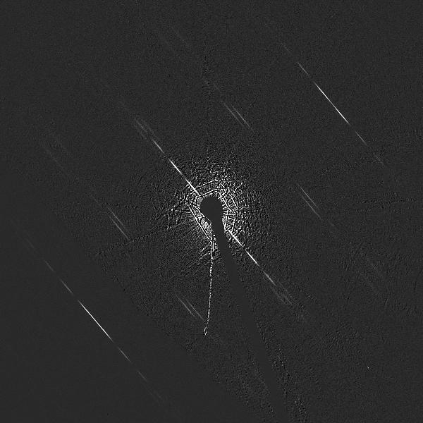
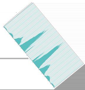
15 Forming an EDP of a SWCNT in TEM Normal incidence --- H Jiang et al, PRB 74 (2006), Incident electrons a carbon nanotube (real space) O.L. Intensities? line spacings? (geometry) The CNT reciprocal countpart tube axis Planar Ewald sphere Layer-lines: intensity analysis --- H Jiang et al, PRB 74 (2006), L 2 L 1 L 0 ( D R) 2 J 0 p 0 ( D R) J 2 n p 0 ( D R) J 2 p m 0 d L 0 Profile L1 Profile L2 Profile 15


, 662 x i")
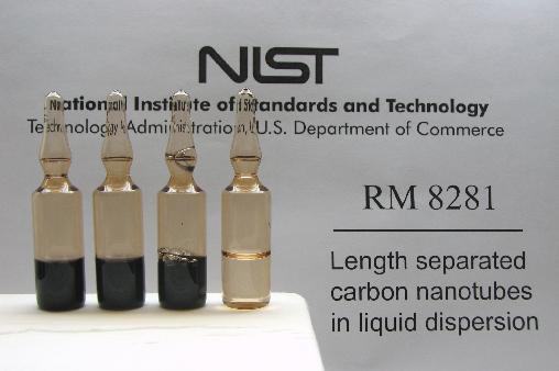
16 Layer-lines: geometry analysis --- H Jiang et al, CARBON 45 (2007), 662 x i = d i d Totally calibration-free An Example NIST VAMAS TWA-34 SWCNT sample Hua Jiang 2010 (6, 5) d 2 d 3 16


17 1,0 2,0 3,0 4,0 5,0 6,0 7,0 8,0 9,0 10,0 11,0 12,0 13,0 14,0 15,0 16,0 17,0 1,1 2,1 3,1 4,1 5,1 6,1 7,1 8,1 9,1 10,1 11,1 12,1 13,1 14,1 15,1 16,1 2,2 3,2 4,2 3,3 5,2 6,2 7,2 8,2 9,2 10,2 11,2 12,2 13,2 14,2 15,2 16,2 4,3 5,3 6,3 7,3 8,3 9,3 10,3 11,3 12,3 13,3 14,3 15,3 4,4 The Chirality map was determined from the EDPs of 49 individual nanotubes: Metallic tubes: 14% Semiconducting tubes: 86% 5,4 6,4 7,4 8,4 9,4 10,4 11,4 12,4 13,4 14,4 15,4 5,5 6,5 7,5 8,5 9,5 10,5 11,5 12,5 13,5 14,5 6,6 7,6 8,6 9,6 10,6 11,6 12,6 13,6 14, nm 7,7 8,7 9,7 10,7 11,7 12,7 13,7 1 nm 8,8 9,8 10,8 11,8 12,8 13,8 9,9 10,9 11,9 12,9 10,10 11,10 12,10 11,11 NIST VAMAS TWA-34 SWCNT sample Hua Jiang 2010 A diffraction pattern can be misleading Combining imaging and diffraction: We see what we diffract!! 17


18 An image may also mislead us The resolution is important in interpreting an image correctly. 2 nm Cs-corrected HREM analysis of a DWCNT taken at 80kV nm 2 nm (32, (17, 10) 18


19 How do CNTs grow? CO as carrier gas and carbon source with ferrocene and CO 2 Fe nanoparticles are formed by thermal decomposition of ferrocene SWCNTs are grown in the gas flow via Bouduard reaction: Fe CO + CO = C(s) + CO 2 Controlled concentration ~ particles/cm 3 High individual SWCNT fraction SWCNT networks formed by filtration at the reactor outlet The TEM sample was collected by placing a grid on filter during collection (collection time: 30 sec.) CO 2 TEM grid 880 C How do CNTs grow from nano-catalyst particles? 19

20 Seeing is believing A TEM shoots not only still images but also movies --- an in-situ study TEM: a few highlights In a conventional TEM, coherent electrons are spread onto a thin (or small) object. They pass though the sample, and carry its structural information. Assisted by the objective lens in the microscope, they form: Electron diffraction pattern (EDP) Electronic micrograph (image) Both image and EDP analysis can mislead us, unless we understand things and do things correctly. TEM is not just an imaging tool, but can also be utilized as a chemical reactor, where one can introduce chemical reaction, and observe the reaction process in real time. As an example, we can grow CNTs in an electron microscope and observe the growth process. 20
Characterisation of Catalysts Using Secondary and Backscattered Electron In-lens Detectors
 Platinum Metals Rev., 2014, 58, (2), 106 110 FINAL ANALYSIS Characterisation of Catalysts Using Secondary and Backscattered Electron In-lens Detectors Heterogeneous catalysis often involves the use of
Microscopy: Principles
 Low Voltage Electron Microscopy: Principles and Applications Edited by David C. Bell Harvard University, USA and Natasha Erdman JEOL USA Inc., USA Published in association with the Royal Microscopical
Nanoelectronics 09. Atsufumi Hirohata Department of Electronics. Quick Review over the Last Lecture
 Nanoelectronics 09 Atsufumi Hirohata Department of Electronics 13:00 Monday, 12/February/2018 (P/T 006) Quick Review over the Last Lecture ( Field effect transistor (FET) ): ( Drain ) current increases
Techniques EDX, EELS et HAADF en TEM: possibilités d analyse et applications
 Techniques EDX, EELS et HAADF en TEM: possibilités d analyse et applications Thomas Neisius Université Paul Cézanne Plan Imaging modes HAADF Example: supported Pt nanoparticles Electron sample interaction
Chapter 9. Electron mean free path Microscopy principles of SEM, TEM, LEEM
 Chapter 9 Electron mean free path Microscopy principles of SEM, TEM, LEEM 9.1 Electron Mean Free Path 9. Scanning Electron Microscopy (SEM) -SEM design; Secondary electron imaging; Backscattered electron
MT Electron microscopy Scanning electron microscopy and electron probe microanalysis
 MT-0.6026 Electron microscopy Scanning electron microscopy and electron probe microanalysis Eero Haimi Research Manager Outline 1. Introduction Basics of scanning electron microscopy (SEM) and electron
HOW TO APPROACH SCANNING ELECTRON MICROSCOPY AND ENERGY DISPERSIVE SPECTROSCOPY ANALYSIS. SCSAM Short Course Amir Avishai
 HOW TO APPROACH SCANNING ELECTRON MICROSCOPY AND ENERGY DISPERSIVE SPECTROSCOPY ANALYSIS SCSAM Short Course Amir Avishai RESEARCH QUESTIONS Sea Shell Cast Iron EDS+SE Fe Cr C Objective Ability to ask the
Analytical Methods for Materials
 Analytical Methods for Materials Lesson 21 Electron Microscopy and X-ray Spectroscopy Suggested Reading Leng, Chapter 3, pp. 83-126; Chapter 4, pp. 127-160; Chapter 6, pp. 191-219 P.J. Goodhew, J. Humphreys
Transmission Electron Microscopy
 L. Reimer H. Kohl Transmission Electron Microscopy Physics of Image Formation Fifth Edition el Springer Contents 1 Introduction... 1 1.1 Transmission Electron Microscopy... 1 1.1.1 Conventional Transmission
The Basic of Transmission Electron Microscope. Text book: Transmission electron microscopy by David B Williams & C. Barry Carter.
 The Basic of Transmission Electron Microscope Text book: Transmission electron microscopy by David B Williams & C. Barry Carter. 2009, Springer Background survey http://presemo.aalto.fi/tem1 Microscopy
Chemical Analysis in TEM: XEDS, EELS and EFTEM. HRTEM PhD course Lecture 5
 Chemical Analysis in TEM: XEDS, EELS and EFTEM HRTEM PhD course Lecture 5 1 Part IV Subject Chapter Prio x-ray spectrometry 32 1 Spectra and mapping 33 2 Qualitative XEDS 34 1 Quantitative XEDS 35.1-35.4
CBE Science of Engineering Materials. Scanning Electron Microscopy (SEM)
") CBE 30361 Science of Engineering Materials Scanning Electron Microscopy (SEM) Scale of Structure Organization Units: micrometer = 10-6 m = 1µm nanometer= 10-9 m = 1nm Angstrom = 10-10 m = 1Å A hair is
CBE 30361 Science of Engineering Materials Scanning Electron Microscopy (SEM) Scale of Structure Organization Units: micrometer = 10-6 m = 1µm nanometer= 10-9 m = 1nm Angstrom = 10-10 m = 1Å A hair is
Scanning Electron Microscopy
 Scanning Electron Microscopy Field emitting tip Grid 2kV 100kV Anode ZEISS SUPRA Variable Pressure FESEM Dr Heath Bagshaw CMA bagshawh@tcd.ie Why use an SEM? Fig 1. Examples of features resolvable using
h p λ = mν Back to de Broglie and the electron as a wave you will learn more about this Equation in CHEM* 2060
 Back to de Broglie and the electron as a wave λ = mν h = h p you will learn more about this Equation in CHEM* 2060 We will soon see that the energies (speed for now if you like) of the electrons in the
AP5301/ Name the major parts of an optical microscope and state their functions.
 Review Problems on Optical Microscopy AP5301/8301-2015 1. Name the major parts of an optical microscope and state their functions. 2. Compare the focal lengths of two glass converging lenses, one with
Transmission Electron Microscopy. Part #2 High Resolution Imaging XEDS EELS spectroscopies Aberration corrected TEM
 Transmission Electron Microscopy Part #2 High Resolution Imaging XEDS EELS spectroscopies Aberration corrected TEM Nicolas Menguy Institut de Minéralogie, de Physique des Matériaux et de Cosmochimie Part
CHEM 681 Seminar Mingqi Zhao April 20, 1998 Room 2104, 4:00 p.m. High Resolution Transmission Electron Microscopy: theories and applications
 CHEM 681 Seminar Mingqi Zhao April 20, 1998 Room 2104, 4:00 p.m. High Resolution Transmission Electron Microscopy: theories and applications In materials science, people are always interested in viewing
Electron Microscopy I
 Characterization of Catalysts and Surfaces Characterization Techniques in Heterogeneous Catalysis Electron Microscopy I Introduction Properties of electrons Electron-matter interactions and their applications
MSE 321 Structural Characterization
 Auger Spectroscopy Auger Electron Spectroscopy (AES) Scanning Auger Microscopy (SAM) Incident Electron Ejected Electron Auger Electron Initial State Intermediate State Final State Physical Electronics
Imaging Carbon materials with correlative Raman-SEM microscopy. Introduction. Raman, SEM and FIB within one chamber. Diamond.
 Imaging Carbon materials with correlative Raman-SEM microscopy Application Example Carbon materials are widely used in many industries for their exceptional properties. Electric conductance, light weight,
Scanning Electron Microscopy & Ancillary Techniques
 Scanning Electron Microscopy & Ancillary Techniques By Pablo G. Caceres-Valencia The prototype of the first Stereoscan supplied by the Cambridge Instrument Company to the dupont Company, U.S.A. (1965)
Supporting Information s for
 Supporting Information s for # Self-assembling of DNA-templated Au Nanoparticles into Nanowires and their enhanced SERS and Catalytic Applications Subrata Kundu* and M. Jayachandran Electrochemical Materials
Massachusetts Institute of Technology. Dr. Nilanjan Chatterjee
 Massachusetts Institute of Technology Dr. Nilanjan Chatterjee Electron Probe Micro-Analysis (EPMA) Imaging and micrometer-scale chemical compositional analysis of solids Signals produced in The Electron
Chapter 12. Nanometrology. Oxford University Press All rights reserved.
 Chapter 12 Nanometrology Introduction Nanometrology is the science of measurement at the nanoscale level. Figure illustrates where nanoscale stands in relation to a meter and sub divisions of meter. Nanometrology
Imaging Methods: Scanning Force Microscopy (SFM / AFM)
") Imaging Methods: Scanning Force Microscopy (SFM / AFM) The atomic force microscope (AFM) probes the surface of a sample with a sharp tip, a couple of microns long and often less than 100 Å in diameter.
Imaging Methods: Scanning Force Microscopy (SFM / AFM) The atomic force microscope (AFM) probes the surface of a sample with a sharp tip, a couple of microns long and often less than 100 Å in diameter.
Surface Sensitivity & Surface Specificity
 Surface Sensitivity & Surface Specificity The problems of sensitivity and detection limits are common to all forms of spectroscopy. In its simplest form, the question of sensitivity boils down to whether
ECE Semiconductor Device and Material Characterization
 ECE 4813 Semiconductor Device and Material Characterization Dr. Alan Doolittle School of Electrical and Computer Engineering Georgia Institute of Technology As with all of these lecture slides, I am indebted
EDS User School. Principles of Electron Beam Microanalysis
 EDS User School Principles of Electron Beam Microanalysis Outline 1.) Beam-specimen interactions 2.) EDS spectra: Origin of Bremsstrahlung and characteristic peaks 3.) Moseley s law 4.) Characteristic
Electron-Matter Interactions
 Electron-Matter Interactions examples of typical EM studies properties of electrons elastic electron-matter interactions scattering processes; coherent and incoherent image formation; chemical contrast;
Gaetano L Episcopo. Scanning Electron Microscopy Focus Ion Beam and. Pulsed Plasma Deposition
 Gaetano L Episcopo Scanning Electron Microscopy Focus Ion Beam and Pulsed Plasma Deposition Hystorical background Scientific discoveries 1897: J. Thomson discovers the electron. 1924: L. de Broglie propose
MEMS Metrology. Prof. Tianhong Cui ME 8254
 MEMS Metrology Prof. Tianhong Cui ME 8254 What is metrology? Metrology It is the science of weights and measures Refers primarily to the measurements of length, weight, time, etc. Mensuration- A branch
= 6 (1/ nm) So what is probability of finding electron tunneled into a barrier 3 ev high?
 So what is probability of finding electron tunneled into a barrier 3 ev high?") STM STM With a scanning tunneling microscope, images of surfaces with atomic resolution can be readily obtained. An STM uses quantum tunneling of electrons to map the density of electrons on the surface
STM STM With a scanning tunneling microscope, images of surfaces with atomic resolution can be readily obtained. An STM uses quantum tunneling of electrons to map the density of electrons on the surface
MS482 Materials Characterization ( 재료분석 ) Lecture Note 4: XRF
 Lecture Note 4: XRF") 2016 Fall Semester MS482 Materials Characterization ( 재료분석 ) Lecture Note 4: XRF Byungha Shin Dept. of MSE, KAIST 1 Course Information Syllabus 1. Overview of various characterization techniques (1 lecture)
2016 Fall Semester MS482 Materials Characterization ( 재료분석 ) Lecture Note 4: XRF Byungha Shin Dept. of MSE, KAIST 1 Course Information Syllabus 1. Overview of various characterization techniques (1 lecture)
ABC s of Electrochemistry series Materials Characterization techniques: SEM and EDS Ana María Valenzuela-Muñiz November 3, 2011
 ABC s of Electrochemistry series Materials Characterization techniques: SEM and EDS Ana María Valenzuela-Muñiz November 3, 2011 CEER, Department of Chemical and Biomolecular Engineering Outline Introduction
Weak-Beam Dark-Field Technique
 Basic Idea recall bright-field contrast of dislocations: specimen close to Bragg condition, s î 0 Weak-Beam Dark-Field Technique near the dislocation core, some planes curved to s = 0 ) strong Bragg reflection
Electron Microprobe Analysis 1 Nilanjan Chatterjee, Ph.D. Principal Research Scientist
 12.141 Electron Microprobe Analysis 1 Nilanjan Chatterjee, Ph.D. Principal Research Scientist Massachusetts Institute of Technology Electron Microprobe Facility Department of Earth, Atmospheric and Planetary
Electron Microprobe Analysis 1 Nilanjan Chatterjee, Ph.D. Principal Research Scientist
 12.141 Electron Microprobe Analysis 1 Nilanjan Chatterjee, Ph.D. Principal Research Scientist Massachusetts Institute of Technology Electron Microprobe Facility Department of Earth, Atmospheric and Planetary
MSE 321 Structural Characterization
 Auger Spectroscopy Auger Electron Spectroscopy (AES) Scanning Auger Microscopy (SAM) Incident Electron Ejected Electron Auger Electron Initial State Intermediate State Final State Physical Electronics
Overview of scattering, diffraction & imaging in the TEM
 Overview of scattering, diffraction & imaging in the TEM Eric A. Stach Purdue University Scattering Electrons, photons, neutrons Radiation Elastic Mean Free Path (Å)( Absorption Length (Å)( Minimum Probe
Auger Electron Spectroscopy
 Auger Electron Spectroscopy Auger Electron Spectroscopy is an analytical technique that provides compositional information on the top few monolayers of material. Detect all elements above He Detection
April 10th-12th, 2017
 Thomas LaGrange, Ph.D. Faculty Lecturer and Senior Staff Scientist Introduction: Basics of Transmission Electron Microscopy (TEM) TEM Doctoral Course MS-637 April 10th-12th, 2017 Outline 1. What is microcopy?
Electron Microprobe Analysis and Scanning Electron Microscopy
 Electron Microprobe Analysis and Scanning Electron Microscopy Electron microprobe analysis (EMPA) Analytical technique in which a beam of electrons is focused on a sample surface, producing X-rays from
Auger Electron Spectroscopy Overview
 Auger Electron Spectroscopy Overview Also known as: AES, Auger, SAM 1 Auger Electron Spectroscopy E KLL = E K - E L - E L AES Spectra of Cu EdN(E)/dE Auger Electron E N(E) x 5 E KLL Cu MNN Cu LMM E f E
Basic structure of SEM
 Table of contents Basis structure of SEM SEM imaging modes Comparison of ordinary SEM and FESEM Electron behavior Electron matter interaction o Elastic interaction o Inelastic interaction o Interaction
3D Boron doped Carbon Nanorods/Carbon-Microfiber Hybrid Composites: Synthesis and Applications as Highly Stable Proton Exchange Membrane Fuel Cell
 Electronic Supplementary Information for Journal of Materials Chemistry 3D Boron doped Carbon Nanorods/Carbon-Microfiber Hybrid Composites: Synthesis and Applications as Highly Stable Proton Exchange Membrane
Praktikum zur. Materialanalytik
 Praktikum zur Materialanalytik Energy Dispersive X-ray Spectroscopy B513 Stand: 19.10.2016 Contents 1 Introduction... 2 2. Fundamental Physics and Notation... 3 2.1. Alignments of the microscope... 3 2.2.
SEM stands for Scanning Electron Microscopy. The earliest known work describing
 1. HISTORY ABOUT SEM SEM stands for Scanning Electron Microscopy. The earliest known work describing the concept of a Scanning Electron Microscope was by M. Knoll (1935) who, along with other pioneers
EE 527 MICROFABRICATION. Lecture 5 Tai-Chang Chen University of Washington
 EE 527 MICROFABRICATION Lecture 5 Tai-Chang Chen University of Washington MICROSCOPY AND VISUALIZATION Electron microscope, transmission electron microscope Resolution: atomic imaging Use: lattice spacing.
2 Symmetry. 2.1 Structure of carbon nanotubes
 2 Symmetry Carbon nanotubes are hollow cylinders of graphite sheets. They can be viewed as single molecules, regarding their small size ( nm in diameter and µm length), or as quasi-one dimensional crystals
Lecture 5. X-ray Photoemission Spectroscopy (XPS)
") Lecture 5 X-ray Photoemission Spectroscopy (XPS) 5. Photoemission Spectroscopy (XPS) 5. Principles 5.2 Interpretation 5.3 Instrumentation 5.4 XPS vs UV Photoelectron Spectroscopy (UPS) 5.5 Auger Electron
Lecture 5 X-ray Photoemission Spectroscopy (XPS) 5. Photoemission Spectroscopy (XPS) 5. Principles 5.2 Interpretation 5.3 Instrumentation 5.4 XPS vs UV Photoelectron Spectroscopy (UPS) 5.5 Auger Electron
Low Voltage Field Emission SEM (LV FE-SEM): A Promising Imaging Approach for Graphene Samples
: A Promising Imaging Approach for Graphene Samples") Low Voltage Field Emission SEM (LV FE-SEM): A Promising Imaging Approach for Graphene Samples Jining Xie Agilent Technologies May 23 rd, 2012 www.agilent.com/find/nano Outline 1. Introduction 2. Agilent
Low Voltage Field Emission SEM (LV FE-SEM): A Promising Imaging Approach for Graphene Samples Jining Xie Agilent Technologies May 23 rd, 2012 www.agilent.com/find/nano Outline 1. Introduction 2. Agilent
SEM. Chemical Analysis in the. Elastic and Inelastic scattering. Chemical analysis in the SEM. Chemical analysis in the SEM
 THE UNIVERSITY Chemical Analysis in the SEM Ian Jones Centre for Electron Microscopy OF BIRMINGHAM Elastic and Inelastic scattering Electron interacts with one of the orbital electrons Secondary electrons,
Nucleation model for chiral-selective growth of SWCNTs
 Nucleation model for chiral-selective growth of SWCNTs William Molden 1, Dr. Venkat Bhethanabotla 2, Debosruti Dutta 2 1 Ursinus College, dept. of Physics 2 University of South Florida, dept. of Chemical
SOLID STATE PHYSICS PHY F341. Dr. Manjuladevi.V Associate Professor Department of Physics BITS Pilani
 SOLID STATE PHYSICS PHY F341 Dr. Manjuladevi.V Associate Professor Department of Physics BITS Pilani 333031 manjula@bits-pilani.ac.in Characterization techniques SEM AFM STM BAM Outline What can we use
Surface Analysis. Dr. Lynn Fuller Dr. Fuller s Webpage:
 ROCHESTER INSTITUTE OF TECHNOLOGY MICROELECTRONIC ENGINEERING Surface Analysis Dr. Lynn Fuller Dr. Fuller s Webpage: http://people.rit.edu/lffeee 82 Lomb Memorial Drive Rochester, NY 14623-5604 Tel (585)
Supplementary Information. Large Scale Graphene Production by RF-cCVD Method
 Supplementary Information Large Scale Graphene Production by RF-cCVD Method Enkeleda Dervishi, *a,b Zhongrui Li, b Fumiya Watanabe, b Abhijit Biswas, c Yang Xu, b Alexandru R. Biris, d Viney Saini, a,b
Structure of Surfaces
 Structure of Surfaces C Stepped surface Interference of two waves Bragg s law Path difference = AB+BC =2dsin ( =glancing angle) If, n =2dsin, constructive interference Ex) in a cubic lattice of unit cell
KMÜ 396 MATERIALS SCIENCE AND TECH. I PRESENTATION ELECTRON ENERGY LOSS SPECTROSCOPY (EELS) TUĞÇE SEZGİN
 TUĞÇE SEZGİN") KMÜ 396 MATERIALS SCIENCE AND TECH. I PRESENTATION ELECTRON ENERGY LOSS SPECTROSCOPY (EELS) TUĞÇE SEZGİN 20970725 HACETTEPE UNIVERSITY DEPARTMENT OF CHEMICAL ENGINEERING, SPRING 2011,APRIL,ANKARA CONTENTS
KMÜ 396 MATERIALS SCIENCE AND TECH. I PRESENTATION ELECTRON ENERGY LOSS SPECTROSCOPY (EELS) TUĞÇE SEZGİN 20970725 HACETTEPE UNIVERSITY DEPARTMENT OF CHEMICAL ENGINEERING, SPRING 2011,APRIL,ANKARA CONTENTS
Controllable Atomic Scale Patterning of Freestanding Monolayer. Graphene at Elevated Temperature
 Controllable Atomic Scale Patterning of Freestanding Monolayer Graphene at Elevated Temperature AUTHOR NAMES Qiang Xu 1, Meng-Yue Wu 1, Grégory F. Schneider 1, Lothar Houben 2, Sairam K. Malladi 1, Cees
PH575 Spring Lecture #28 Nanoscience: the case study of graphene and carbon nanotubes.
 PH575 Spring 2014 Lecture #28 Nanoscience: the case study of graphene and carbon nanotubes. Nanoscience scale 1-100 nm "Artificial atoms" Small size => discrete states Large surface to volume ratio Bottom-up
Lecture 5: Characterization methods
 Lecture 5: Characterization methods X-Ray techniques Single crystal X-Ray Diffration (XRD) Powder XRD Thin film X-Ray Reflection (XRR) Microscopic methods Optical microscopy Electron microscopies (SEM,
tip conducting surface
 PhysicsAndMathsTutor.com 1 1. The diagram shows the tip of a scanning tunnelling microscope (STM) above a conducting surface. The tip is at a potential of 1.0 V relative to the surface. If the tip is sufficiently
CHARACTERIZATION of NANOMATERIALS KHP
 CHARACTERIZATION of NANOMATERIALS Overview of the most common nanocharacterization techniques MAIN CHARACTERIZATION TECHNIQUES: 1.Transmission Electron Microscope (TEM) 2. Scanning Electron Microscope
ABNORMAL X-RAY EMISSION FROM INSULATORS BOMBARDED WITH LOW ENERGY IONS
 302 ABNORMAL X-RAY EMISSION FROM INSULATORS BOMBARDED WITH LOW ENERGY IONS M. Song 1, K. Mitsuishi 1, M. Takeguchi 1, K. Furuya 1, R. C. Birtcher 2 1 High Voltage Electron Microscopy Station, National
Nanoscale Chemical Characterization: Moving to 3 Dimensions
 Nanoscale Chemical Characterization: Moving to 3 Dimensions Eric B. Steel Chemical Science & Technology Laboratory National Institute of Standards & Technology Outline What is and why do we need chemical
Structure analysis: Electron diffraction LEED TEM RHEED
 Structure analysis: Electron diffraction LEED: Low Energy Electron Diffraction SPA-LEED: Spot Profile Analysis Low Energy Electron diffraction RHEED: Reflection High Energy Electron Diffraction TEM: Transmission
In the name of Allah
 In the name of Allah Nano chemistry- 4 th stage Lecture No. 1 History of nanotechnology 16-10-2016 Assistance prof. Dr. Luma Majeed Ahmed lumamajeed2013@gmail.com, luma.ahmed@uokerbala.edu.iq Nano chemistry-4
Fundamentals of Nanoscale Film Analysis
 Fundamentals of Nanoscale Film Analysis Terry L. Alford Arizona State University Tempe, AZ, USA Leonard C. Feldman Vanderbilt University Nashville, TN, USA James W. Mayer Arizona State University Tempe,
Characterization of zeolites by advanced SEM/STEM techniques
 SCIENTIFIC INSTRUMENT NEWS 2016 Vol. 7 SEPTEMBER Technical magazine of Electron Microscope and Analytical Instruments. Article Characterization of zeolites by advanced SEM/STEM techniques Toshiyuki Yokoi
APPLICATION OF THE NUCLEAR REACTION ANALYSIS FOR AGING INVESTIGATIONS
 1 APPLICATION OF THE NUCLEAR REACTION ANALYSIS FOR AGING INVESTIGATIONS G.Gavrilov, A.Krivchitch, V.Lebedev PETERSBURG NUCLEAR PHYSICS INSTITUTE E-mail: lebedev@pnpi.spb.ru kriv@rec03.pnpi.spb.ru We used
Chapter 10. Nanometrology. Oxford University Press All rights reserved.
 Chapter 10 Nanometrology Oxford University Press 2013. All rights reserved. 1 Introduction Nanometrology is the science of measurement at the nanoscale level. Figure illustrates where nanoscale stands
Information from Every Angle
 pplication Note Information from Every ngle Directional SE Detector for Next-Level Imaging Zinc oxide nanorods with surficial palladium particles imaged at 500 V in high vacuum. dding palladium increases
Instantaneous reduction of graphene oxide at room temperature
 Instantaneous reduction of graphene oxide at room temperature Barun Kuma Burman, Pitamber Mahanandia and Karuna Kar Nanda Materials Research Centre, Indian Institute of Science, Bangalore-560012, India
6. Analytical Electron Microscopy
 Physical Principles of Electron Microscopy 6. Analytical Electron Microscopy Ray Egerton University of Alberta and National Institute of Nanotechnology Edmonton, Canada www.tem-eels.ca regerton@ualberta.ca
MT Electron microscopy Scanning electron microscopy and electron probe microanalysis
 MT-0.6026 Electron microscopy Scanning electron microscopy and electron probe microanalysis Eero Haimi Research Manager Outline 1. Introduction Basics of scanning electron microscopy (SEM) and electron
MS482 Materials Characterization ( 재료분석 ) Lecture Note 2: UPS
 Lecture Note 2: UPS") 2016 Fall Semester MS482 Materials Characterization ( 재료분석 ) Lecture Note 2: UPS Byungha Shin Dept. of MSE, KAIST 1 Course Information Syllabus 1. Overview of various characterization techniques (1 lecture)
2016 Fall Semester MS482 Materials Characterization ( 재료분석 ) Lecture Note 2: UPS Byungha Shin Dept. of MSE, KAIST 1 Course Information Syllabus 1. Overview of various characterization techniques (1 lecture)
MS482 Materials Characterization ( 재료분석 ) Lecture Note 11: Scanning Probe Microscopy. Byungha Shin Dept. of MSE, KAIST
 Lecture Note 11: Scanning Probe Microscopy. Byungha Shin Dept. of MSE, KAIST") 2015 Fall Semester MS482 Materials Characterization ( 재료분석 ) Lecture Note 11: Scanning Probe Microscopy Byungha Shin Dept. of MSE, KAIST 1 Course Information Syllabus 1. Overview of various characterization
2015 Fall Semester MS482 Materials Characterization ( 재료분석 ) Lecture Note 11: Scanning Probe Microscopy Byungha Shin Dept. of MSE, KAIST 1 Course Information Syllabus 1. Overview of various characterization
A NEW APPROACH TOWARDS PROPERTY NANOMEASUREMENTS USING IN-SITU TEM
 A NEW APPROACH TOWARDS PROPERTY NANOMEASUREMENTS USING IN-SITU TEM Z.L. WANG*, P. PONCHARAL**, W.A. DE HEER** and R.P. GAO* * School of Materials Science and Engineering, ** School of Physics, Georgia
Nano-Microscopy. Lecture 2. Scanning and Transmission Electron Microscopies: Principles. Pavel Zinin HIGP, University of Hawaii, Honolulu, USA
 GG 711: Advanced Techniques in Geophysics and Materials Science Nano-Microscopy. Lecture 2 Scanning and Transmission Electron Microscopies: Principles Pavel Zinin HIGP, University of Hawaii, Honolulu,
Applied Physics - II
 F.E. Sem. II Applied Physics - II Time : Hrs.] Prelim Question Paper Solution [Marks : 60 Q.1 Attempt any Five questions of the following : [15] Q.1(a) Fringes of equal thickness are observed in a thin
Why microscopy?
 Electron Microscopy Why microscopy? http://www.cellsalive.com/howbig.htm 2 Microscopes are used as magnifying tools (although not exclusively as will see later on). The resolution of the human eye is limited
Electron and electromagnetic radiation
 Electron and electromagnetic radiation Generation and interactions with matter Stimuli Interaction with sample Response Stimuli Waves and energy The energy is propotional to 1/λ and 1/λ 2 λ λ 1 Electromagnetic
Fabrication and characterization of poly (ethylene oxide) templated nickel oxide nanofibers for dye degradation
 templated nickel oxide nanofibers for dye degradation") Electronic Supplementary Material (ESI) for Environmental Science: Nano. This journal is The Royal Society of Chemistry 2014 Supplementary Information Fabrication and characterization of poly (ethylene
Electronic Supplementary Material (ESI) for Environmental Science: Nano. This journal is The Royal Society of Chemistry 2014 Supplementary Information Fabrication and characterization of poly (ethylene
Conventional Transmission Electron Microscopy. Introduction. Text Books. Text Books. EMSE-509 CWRU Frank Ernst
 Text Books Conventional Transmission Electron Microscopy EMSE-509 CWRU Frank Ernst D. B. Williams and C. B. Carter: Transmission Electron Microscopy, New York: Plenum Press (1996). L. Reimer: Transmission
Photoemission Electron Microscopy (PEEM)
") PHOTOEMISSION ELECTRON MICROSCOPY Pat Photongkam Research Facility Division Synchrotron Light Research Institute (Public Organization) Synchrotron Light Research Institute (Public Organization) 111 University
PHOTOEMISSION ELECTRON MICROSCOPY Pat Photongkam Research Facility Division Synchrotron Light Research Institute (Public Organization) Synchrotron Light Research Institute (Public Organization) 111 University
Depth Distribution Functions of Secondary Electron Production and Emission
 Depth Distribution Functions of Secondary Electron Production and Emission Z.J. Ding*, Y.G. Li, R.G. Zeng, S.F. Mao, P. Zhang and Z.M. Zhang Hefei National Laboratory for Physical Sciences at Microscale
IMAGING DIFFRACTION SPECTROSCOPY
 TEM Techniques TEM/STEM IMAGING DIFFRACTION SPECTROSCOPY Amplitude contrast (diffracion contrast) Phase contrast (highresolution imaging) Selected area diffraction Energy dispersive X-ray spectroscopy
Synthesis of Colloidal Au-Cu 2 S Heterodimers via Chemically Triggered Phase Segregation of AuCu Nanoparticles
 SUPPORTING INFORMATION Synthesis of Colloidal Au-Cu 2 S Heterodimers via Chemically Triggered Phase Segregation of AuCu Nanoparticles Nathan E. Motl, James F. Bondi, and Raymond E. Schaak* Department of
Characterisation of atmospheric aerosol sampled from an aircraft using scanning electron microscopy
 School of Earth and Environment INSTITUTE FOR CLIMATE & ATMOSPHERIC SCIENCE Characterisation of atmospheric aerosol sampled from an aircraft using scanning electron microscopy Alberto Sánchez-Marroquín,
Part II: Thin Film Characterization
 Part II: Thin Film Characterization General details of thin film characterization instruments 1. Introduction to Thin Film Characterization Techniques 2. Structural characterization: SEM, TEM, AFM, STM
Elastic and Inelastic Scattering in Electron Diffraction and Imaging
 Elastic and Inelastic Scattering in Electron Diffraction and Imaging Contents Introduction Symbols and definitions Part A Diffraction and imaging of elastically scattered electrons Chapter 1. Basic kinematical
Supplementary Information
 Supplementary Information Time-dependent growth of zinc hydroxide nanostrands and their crystal structure Xinsheng Peng, ab Jian Jin, a Noriko Kobayashi, a Wolfgang Schmitt, c and Izumi Ichinose* a a Organic
Transmission Electron Microscopy. Part #1 Diffraction Conventional Imaging
 Transmission Electron Microscopy Part #1 Diffraction Conventional Imaging Nicolas Menguy Institut de Minéralogie, de Physique des Matériaux et de Cosmochimie Outline Part 1 : Conventional TEM - Transmission
Characterization Tools
 Lectures in Nanoscience & Technology Characterization Tools K. Sakkaravarthi Department of Physics National Institute of Technology Tiruchirappalli 620 015 Tamil Nadu India sakkaravarthi@nitt.edu ksakkaravarthi.weebly.com
Raman spectroscopy study of rotated double-layer graphene: misorientation angle dependence of electronic structure
 Supplementary Material for Raman spectroscopy study of rotated double-layer graphene: misorientation angle dependence of electronic structure Kwanpyo Kim 1,2,3, Sinisa Coh 1,3, Liang Z. Tan 1,3, William
Supplementary information
 Supplementary information Supplementary Figures Supplementary Figure 1. CO 2 light off curve obtained from the 5 wt% Pt/Al 2 O 3 catalyst obtained through heating the catalyst under a 50 ml.min -1 flow
Everhart-Thornley detector
 SEI Detector Everhart-Thornley detector Microscope chamber wall Faraday cage Scintillator Electrons in Light pipe Photomultiplier Electrical signal out Screen Quartz window +200 V +10 kv Always contains
MICRO-TOMOGRAPHY AND X-RAY ANALYSIS OF GEOLOGICAL SAMPLES
 THE PUBLISHING HOUSE PROCEEDINGS OF THE ROMANIAN ACADEMY, Series A, OF THE ROMANIAN ACADEMY Volume 18, Number 1/2017, pp. 42 49 MICRO-TOMOGRAPHY AND X-RAY ANALYSIS OF GEOLOGICAL SAMPLES Ion GRUIA University
Backscattered Electron Contrast Imaging of Scanning Electron Microscopy for Identifying Double Layered Nano-Scale Elements
 Journal of Surface Analysis Vol.17, No.3 (211) pp.341-345 Paper Backscattered Electron Contrast Imaging of Scanning Electron Microscopy for Identifying Double Layered Nano-Scale Elements Hyonchol Kim,
Highly efficient SERS test strips
 Electronic Supplementary Information (ESI) for Highly efficient SERS test strips 5 Ran Zhang, a Bin-Bin Xu, a Xue-Qing Liu, a Yong-Lai Zhang, a Ying Xu, a Qi-Dai Chen, * a and Hong-Bo Sun* a,b 5 10 Experimental