Nano-Microscopy. Lecture 2. Scanning and Transmission Electron Microscopies: Principles. Pavel Zinin HIGP, University of Hawaii, Honolulu, USA
|
|
|
- Gavin Thomas
- 6 years ago
- Views:
Transcription

1 GG 711: Advanced Techniques in Geophysics and Materials Science Nano-Microscopy. Lecture 2 Scanning and Transmission Electron Microscopies: Principles Pavel Zinin HIGP, University of Hawaii, Honolulu, USA


2 r Airy Why Electrons nsin nna It all started with light, but even with better lenses, oil immersion and short wavelengths, resolution was only about 0.2 mm/1000x = 0.2 m. AFM OM 1 Å 1 nm 1 µm 1 mm 1 cm STM SEM SAM


3 A black body is an idealized physical body that absorbs all incident electromagnetic radiation. Because of this perfect absorptivity at all wavelengths, a black body is also the best possible emitter of thermal radiation, which it radiates incandescently in a characteristic, continuous spectrum that depends on the body's temperature. At Earth-ambient temperatures this emission is in the infrared region of the electromagnetic spectrum and is not visible. The object appears black, since it does not reflect or emit any visible light. Black Body Radiation Sketch of the black body: The opening in the cavity of a body is a good approximation to a black body. As light enters the cavity through the small opening, part is reflected and part is absorbed on each reflection from the interior walls. After many reflections, essentially all of the incident energy is absorbed. The color (chromaticity) of blackbody radiation depends on the temperature of the black body; the locus of such colors, shown here in CIE 1931 x,y space, is known as the Planckian locus (Wikipedia, 2011).

4 Black Body Radiation An object at any temperature is known to emit radiation sometimes referred to as thermal radiation. The characteristics of this radiation depend on the temperature and properties of the object. At low temperatures, the wavelengths of the thermal radiation are mainly in the infrared region and hence are not observed by the eye. As the temperature of the object is increased, it eventually begins to glow red. At sufficiently high temperatures, it appears to be white, as in the glow of the hot tungsten filament of a light bulb. A careful study of thermal radiation shows that it consists of a continuous distribution of wavelengths from the infrared, visible, and ultraviolet portions of the spectrum. As the temperature decreases, the peak of the blackbody radiation curve moves to lower intensities and longer wavelengths. The blackbody radiation graph is also compared with the classical model of Rayleigh and Jeans.

5 Planck Postualte The Planck Postulate (or Planck's Postulate), one of the fundamental principles of quantum mechanics, is the postulate that the energy of oscillators in a black body is quantized, and is given by In his theory, Planck made two assumptions: 1. The vibrating molecules that emitted the radiation could have only certain discrete amounts of energy, E n, given by E nh where n is an integer 1, 2, 3,..., h is Planck's constant, and (the Greek letter) is the frequency of the oscillator. The energies of the molecule are said to be quantized, and the allowed energy states are called quantum states. The factor h is a constant, known as Planck's constant, given by : h = X J. s Max Planck ( ). Nobel Prize in Physics (1918.) 2. The molecules emit energy in discrete units of light energy called quanta (or photons, as they are now called).


6 Application Black Body Radiation Theory Temperature is calculated from the radiation emitted from a material using Planck's blackbody equation: I c 1 5 c2 exp T 1 Temperature can also be calculated using Wien's approximation to Planck's law: J ln T 1 where I is spectral intensity, is emissivity, is wavelength, c1 and c2 are physical constants, and T is temperature. J = ln(i 5 /c 1 ) and = c 2 /. Thus. a linear fit to a spectrum transformed to coordinates of J and yields both temperature (inverse slope) and emissivity (y-intercept). Wien's approximation and Planck's law give nearly identical temperatures up to about 3000 K, but diverge at higher temperatures with Wien's law giving progressively lower values (~ 1 at 5000 K).

7 The Wave Properties of Particles In 1924, the French physicist Louis de Broglie wrote a doctoral dissertation. "The fundamental idea of [my 1924 thesis] was the following: The fact that, following Einstein's introduction of photons in light waves, one knew that light contains particles which are concentrations of energy incorporated into the wave, suggests that all particles, like the electron, must be transported by a wave into which it is incorporated... My essential idea was to extend to all particles the coexistence of waves and particles discovered by Einstein in 1905 in the case of light and photons." "With every particle of matter with mass m and velocity v a real wave must be 'associated'", related to the momentum by the equation: h p h mv Where is the wavelength of particle, h is the Planck's const, m is the particle mass, and v is the particle velocity. From CHEM 793, 2008 Fall
8 Why Electrons An electron microscope is an instrument that uses electrons instead of light for the imaging of objects. The development of the transmission electron microscope was based on theoretical work done by Louis de Broglie, discovered that moving particles have a wave nature. Louis de Broglie found that wavelength of moving particle is inversely proportional to momentum, p: h p h mv Where is the wavelength of particle, h is the Planck's const, m is the particle mass, and v is the particle velocity. Louis-Victor-Pierre- Raymond, 7th duc de Broglie ( ). Nobel Prize in Physics (1929) From CHEM 793, 2008 Fall
9 Why Electrons Electrons have a charge and can be accelerated in an electric potential field as well as focused by electric or magnetic fields. If an electron is accelerated through a potential ev, it gains kinetic energy So the momentum is mv ev mv 2meV Where V (in Volts)is the electrical potential. An electron accelerated in a potential of V volts has kinetic energy m v 2 /2 = e V where e is the charge on the electron. Solving for v and substituting into de Broglie's equation (and expanding in V to account for the fact that the electron mass is different when moving than when at rest): h p h mv v 2eV m 2 h 2m e V
10 Resolution of SEM Substitutin the known values in this equation: h = ; m = ; e = ; e.s.u. We obtain: Then, for the Airy radius we have 2 h meV V Å r Airy nsin nsin V Since electron microscope aperture angles are always very small sin, and since the object and image are in field free space in SEM, the refraction index n = 1. Thus r Airy 7.5 V =10-2 radians, V=10 5 volts r ~ 2.4 Å (Wischnitzer, 1970)
11 Resolution of SEM

12 Electron Microscopy Definition: The scanning electron microscope (SEM) is a type of electron microscope that images the sample surface by scanning it with a high-energy beam of electrons in a raster scan pattern. The electrons interact with the atoms that make up the sample producing signals that contain information about the sample's surface topography, composition and other properties such as electrical (Wikipedia, 2009). Electron microscopes have much greater resolving power than light microscopes that use electromagnetic radiation and can obtain much higher magnifications of up to 2 million times, while the best light microscopes are limited to magnifications of 2000 times.

13 Resolving power line
14 Scanning Electron Microscopy (SEM) Instrumentation - How Does It Work? Essential components of all SEMs include the following: 1.Electron Source ("Gun") 2.Electron Lenses 3.Sample Stage 4.Detectors for all signals of interest 5.Display / Data output devices 6.Infrastructure Requirements: a. Power Supply b. Vacuum System c. Cooling system d. Vibration-free floor e. Room free of ambient magnetic and electric fields SEMs always have at least one detector (usually a secondary electron detector), and most have additional detectors. The specific capabilities of a particular instrument are critically dependent on which detectors it accommodates.
15 Source of Electrons An electron gun (also called electron emitter) is an electrical component that produces an electron beam that has a precise kinetic energy and is most often used in televisions and monitors which use cathode ray tube technology, as well as in other instruments, such as electron microscopes and particle accelerators (Wikipedia, 2009). Principle: A voltage is applied to a tungsten filament (cathode): it is heated and electrons are produced The electrons are accelerated to the anode. Electrons can exit a small (<1mm) hole to move down the EM column (in a vacuum) for imaging

16 The Filament & Thermionic Emission Tungsten wire The tungsten cathode is a fine wire approximately 100mm in diameter that has been bent into the shape of a hairpin with a V-shaped tip. The tip is heated by passing current through it; normally, the tip is heated to around 2400 C. At this temperature, one can expect a current density of approximately 1.75 A/cm 2. The electrons will have a potential distribution of 0 to 2 volts. With a bias voltage between 0 and 500 volts, the electrons can be accelerated toward the anode. An SEM image and a chematic diagram of a tungsten cathode is shown in the Figures. (


17 The Filament & Thermionic Emission LaB 6 As the need for higher resolution imaging increased, so did the need for brighter filaments. The most straightforward method to achieve this goal is to find a material with a lower work function Ew. A lower work function means more electrons at a given temperature, hence a brighter filament and higher resolution. Lanthanum hexaboride, commonly known as LaB 6, has been the best material developed to date for this application. The LaB 6 filament operates at approximately 2125 C, resulting in a brightness on the order of five times brighter than a tungsten filament under the same conditions. LaB 6 filaments tend to be an order of magnitude more expensive than tungsten filaments. A schematic of the LaB 6 filament is shown in Figure

18 Electron Lenses In 1926, Hans Busch discovered that magnetic fields could act as lenses by causing electron beams to converge to a focus. A few years later, Max Knoll and Ernst Ruska made the first modern prototype of an electron microscope A strong magnetic field is generated by passing a current through a set of windings. This field acts as a convex lens, bringing off axis rays back to focus. Focal length can be altered by changing the strength of the current. The image is rotated, to a degree that depends on the strength of the lens.

19 Invention of Scanning Electron Microscope The first electron microscope prototype was built in 1931 by the German engineers Ernst Ruska and Max Knoll. Although this initial instrument was only capable of magnifying objects by four hundred times, it demonstrated the principles of an electron microscope. Two years later, Ruska constructed an electron microscope that exceeded the resolution possible using an optical microscope. SEM or STEM
 was concerned with the mathematical and experimental proof of Busch's theory of the effect of the magnetic field of a coil")
20 Invention of Electron Microscopy Dr. Ernst Ruska at the University of Berlin. The Nobel Prize in Physics 1986 My first completed scientific work (1928-9) was concerned with the mathematical and experimental proof of Busch's theory of the effect of the magnetic field of a coil of wire through which an electric current is passed and which is then used as an electron lens. During the course of this work I recognised that the focal length of the waves could be shortened by use of an iron cap. From this discovery the polschuh lens was developed, a lens which has been used since then in all magnetic high-resolution electron microscopes. Further work, conducted together with Dr Knoll, led to the first construction of an electron microscope in With this instrument two of the most important processes for image reproduction were introduced-the principles of emission and radiation. In 1933 I was able to put into use an electron microscope, built by myself, that for the first time gave better definition than a light microscope. In my Doctoral thesis of 1934 and for my university teaching thesis (1944), both at the Technical College in Berlin, I investigated the properties of electron lenses with short focal lengths. (From Autobiography)
21 Comparison of LM and TEM Both glass and EM lenses subject to same distortions and aberrations Glass lenses have fixed focal length, it requires to change objective lens to change magnification. We move objective lens closer to or farther away from specimen to focus. EM lenses to specimen distance fixed, focal length varied by varying current through lens LM: (a) Direct observation of the image; (b) image is formed by transmitted light TEM: (a) Video imaging (CRT); (b) image is formed by transmitted electrons impinging on phosphor coated screen


22 SEM what do we get? Topography (surface picture) commonly enhanced by sputtering (coating) the sample with gold or carbon SEM Images of Aunt (courtesy to Shruti Tiwari)


23 Advantages of Using SEM over LM The SEM also produces images of high resolution, closely features can be examined at a high magnification. The combination of higher magnification, larger depth of field, greater resolution makes the SEM one of the most heavily used instruments
 are torr and Pascal.")

 No scattering")
24 Electrons Need a Vacuum Units of Vacuum: The two main units used to measure pressure (vacuum) are torr and Pascal. Atmospheric pressure (STD) = 760 torr or 1.01x10 5 Pascal. Vacuum Air One torr = Pascal One Pascal = torr An excellent vacuum in the electron microprobe chamber is 4x10⁻⁵ Pa (which is 3x10⁻⁷ torr) No scattering Complete scattering
25 Scanning Electron Microscope As an electron travels through the interaction volume, it is said to scatter; that is, lose energy and change direction with each atomic interaction. Scattering events can be divided into two general classes: 1. Elastic scattering, in which the electron exchanges little or no energy, but changes direction; 2. Inelastic scattering, in which the electron exchanges significant, and definite, amounts energy, but has its direction virtually unchanged. Both types of events determine the size and shape of the interaction volume. Inelastic scattering events are responsible for the wide variety of characteristic (i.e., element specific) and non-specific information, which can be emitted and detected from the specimen. These include secondary electrons, Augér electrons, characteristic and continuum x-rays, long-wavelength radiation in the visible, IR and UV spectral range (cathodoluminescence), lattice vibrations or phonons, and electron oscillations or plasmons. The inelastic scattering events, because many of them are element specific, are especially useful in quantitative EPMA. For our purposes, the elastic scattering events are important in that they (1) produce backscattered electrons and (2) change the shape of the scattering volume (that is the depth to lateral scattering spatial ratio).
26 Scanning Electron Microscope Elastic scattering occurs when the energy of the scattered electron is the same as the energy of the incident electron, i.e. there is no energy transferred from the beam into the specimen. Elastic scattering causes the beam to diffuse through the sample. Electron beam interactions can be classified into two types of events: elastic interactions and inelastic interactions. Inelastic scattering results when the incident electron loses energy in its interaction with the sample. There are a number of different processes that cause this. They include: plasmon excitation, excitation of conduction electrons leading to secondary electron emission, ionization of inner shells, Bremsstrahlung or Continuum x-rays, and excitation of phonons. Inelastic scattering then, slows the electrons as they penetrate into the sample.
27 Interaction of electrons with matter in an electron microscope Back scatter electrons compositional Secondary electrons topography X-rays chemistry

28 Interaction of Electrons with a thick specimen (SEM) In theory, a higher voltage should give better resolution because of reduction in wavelength of the beam of electrons. However, the volume of the interaction increases with increase accelerating voltage. Therefore, the increase in volume of the region of interaction results in a decrease in resolution. In practice, balance must be achieved in selecting the optimum acceleration voltage. From:Vick Guo, Introduction to Electron Microscopy and Microanalysis


29 Beam Penetration Beam penetration decreases with Z Beam penetration increases with energy Electron range ~ inelastic processes Electron scattering (aspect) ~ elastic processes Secondary electrons ~100A-10nm Backscatter electrons 1-2µm Characteristic X-rays 2-5 m

30 Backscattered electrons (BSE) The resolution of the images is limited by the radius in which the backscattered electrons are produced; the resolution is limited to the order of 2 Radius, irrelevant of the diameter of the incident electron beam. The intensity of the backscattered electron signal is also affected by the composition, in particular any inhomogeneity, in the sample. Backscattered electrons (BSE) consist of highenergy electrons originating in the electron beam, that are reflected or back-scattered out of the specimen interaction volume by elastic scattering interactions with specimen atoms. Since heavy elements (high atomic number) backscatter electrons more strongly than light elements (low atomic number), and thus appear brighter in the image, BSE are used to detect contrast between areas with different chemical compositions. Sketch of backscattered electron detector
 backscattered electron")
, wherein electron-hole pairs are generated and")

31 Backscatter Electron Detection In-Lens and Energy Selective BSE A solid-state (semi-conductor) backscattered electron detector (a) is energized by incident high energy electrons (~90% E 0 ), wherein electron-hole pairs are generated and swept to opposite poles by an applied bias voltage. BSE detector UofO- Geology 619, CAMCOR, UNI Oregon.

 of the single not")
32 Elastic process: Backscattered Electrons SEM image (Backscattering Electrons) of the single not used ICPG granule


33 Backscattering Electron Imaging: Atomic Number Contrast Raney Ni-Al Al-Cu eutectic Obsidian m 2 m 4 10 m Backscatter arises from interaction of electrons with nucleus: atoms with higher mass scatter more. UofO- Geology 619, CAMCOR, UNI Oregon.

34 Secondary Electrons Secondary electrons are defined as those electrons emitted that have an energy of less than 50 ev. Secondary electrons come from the top 1 to 10 nm of material in the sample, with 1nm being more characteristic for metals, and 10 nm being more characteristic for insulators. The secondary electron coefficient tends to be insensitive to atomic number. The secondary electron coefficient is, however, dependent on beam energy. Starting at zero energy, the secondary electron coefficient rises with increasing energy, reaching unity around 1 kev. The curve then peaks at just over 1 for metals and as high as 5 for insulators and then falls below unity between 2 and 3 kev. This region above unity tends to be a good beam energy for performing voltage contrast.

35 Atom Structure and Secondary Electrons The most popular SEM imaging is done by interpreting secondary electrons. When the electron beam scans the sample surface, high-energy electrons from the incident beam interact with valence electrons of the sample atoms. The valence electrons are released from the atom and emerge from the surface, often after traveling through the sample. The emergent electrons with energies less than 50 ev are called secondary electrons.

36 Secondary Electron Images From

37 Comparison of SEM techniques Top: backscattered electron analysis - composition Bottom: secondary electron analysis - topography
38 Secondary Electron Production SE imaging: the signal is from the top 5 nm in metals, and the top 50 nm in insulators. Thus, fine scale surface features are imaged. The detector is located to one side, so there is a shadow effect one side is brighter than the opposite. Detection :Electrons Scintillator photons photomultiplier conversion into electric current detection SE detector Pollen
39 Resolution Limits Imposed by Spherical Aberration, Cs Spherical aberration is the failure of the lens system to image central and peripheral electrons at the same focal point. For Cs > 0, rays far from the axis are bent too strongly and come to a crossover before the gaussian image plane (focus). For a lens with aperture angle α, the minimum blur is min d dmin Typical TEM numbers: C s = 1 mm, α=10 mrad d min = 0.5 nm C s
 spherical aberration is present decreasing resolution (A).")
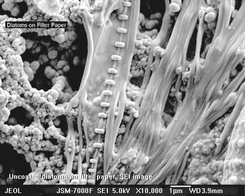
. Bar is 5µm, Magnification = x 3300, Acceleration Voltage = 5kV, Condenser Lens setting = 14 (A and B).")
40 Resolution Limits Imposed by Spherical Aberration, Cs A diatom imaged using different working distances. At a longer working distance (WD = 48mm) spherical aberration is present decreasing resolution (A). At a shorter working distance (WD = 8) the effect of spherical aberration is less resulting in an image with improved resolution (B). Bar is 5µm, Magnification = x 3300, Acceleration Voltage = 5kV, Condenser Lens setting = 14 (A and B).
41 Balancing Spherical Aberration against the Diffraction Limit Evaluation, at electron wavelengths (e.g., nm at 100 kv), of the expressions for limiting resolving power would appear to suggest the possibility of electron- optical resolutions beyond nm. However, several other factors must be con sidered in electron microscopy. In particular, spherical aberration, which can be reduced to negligible levels in glass lenses, remains significant even in the best electron lenses. Feasible aperture angles are therefore small (<10-2 rad), so that the sin = approximation is valid, giving as a general expression for the resolving power of an electron lens. d min 2rmin (1) A first approximation to estimation of attainable resolving power equates the radius of the diffraction figure to the radius of the disc of confusion due to spherical aberration. Ignoring numerical constants, this gives the optimal aperture angle as ( /C) 1/4 and yields, by substitution in eq. (1), d C min 1/ 4 3/ 4 s where C s is the spherical aberration constant. This equation predicts ultimate resolving powers, at 100 kv, on the order of 0.5 nm (E. Slayter, Light and Electron Microscopy).


42 SE and BSE Images SE 20kV BSE SE 5kV BSE

43 Grains in a Polished Fe-Si Alloy by Different SEM methods David Muller 2008, Cornel University


44 kv and Fine Structure 5 kv 25 kv From: UofO- Geology 619


45 Depth of Focus By simply shortening the working distance the background is blurred drawing the viewers eye to the bugs proboscis.

 (B).")
46 SEM Example These backscattered electrons may generate secondary electrons near the sample surface on their way out, increasing the area from which secondary electrons are produced and therefore reducing the resolution of the final image. A diatom imaged using different accelerating voltages. Fine detail of a diatom imaged at a low accelerating voltage of 5kV is visible (A). A decrease in resolution and contrast can be observed when a diatom is imaged using a much higher accelerating voltage (20kV) (B). Bar is 1µm, Magnification = x 4000, Working Distance = 8mm, Condenser Lens setting = 15 (A and B).

47 X-ray Generation and Detection
48 Resolution in SEM and TEM The spatial resolution of the SEM depends on the size of the electron spot, which in turn depends on both the wavelength of the electrons and the electron-optical system which produces the scanning beam. The resolution is also limited by the size of the interaction volume, or the extent to which the material interacts with the electron beam. The spot size and the interaction volume are both large compared to the distances between atoms, so the resolution of the SEM is not high enough to image individual atoms, as is possible in the shorter wavelength (i.e. higher energy) (TEM). Depending on the instrument, the resolution can fall somewhere between less than 1 nm and 20 nm. By 2009, The world's highest SEM resolution at high beam energies (0.4 nm at 30 kv) is obtained with the Hitachi S In a TEM, a monochromatic beam of electrons is accelerated through a potential of 40 to 100 kilovolts (kv) and passed through a strong magnetic field that acts as a lens. The resolution of a modern TEM is about 0.2 nm. This is the typical separation between two atoms in a solid. This resolution is 1,000 times greater than a light microscope and about 500,000 times greater than that of a human eye.
49 Magnification in Scanning Electron Microscopy Magnification in a SEM can be controlled over a range of up to 6 orders of magnitude from about 10 to 500,000 times. Unlike optical and transmission electron microscopes, image magnification in the SEM is not a function of the power of the objective lens. SEMs may have condenser and objective lenses, but their function is to focus the beam to a spot, and not to image the specimen. Provided the electron gun can generate a beam with sufficiently small diameter, a SEM could in principle work entirely without condenser or objective lenses, although it might not be very versatile or achieve very high resolution. In a SEM, as in scanning probe microscopy, magnification results from the ratio of the dimensions of the raster on the specimen and the raster on the display device. Assuming that the display screen has a fixed size, higher magnification results from reducing the size of the raster on the specimen, and vice versa. Magnification is therefore controlled by the current supplied to the x, y scanning coils, or the voltage supplied to the x, y deflector plates, and not by objective lens power.
50 Home Work 1. Describe the Principle of Scanning Electron(SO). 2. Derive Lateral resolution of SEM (KK). 3. Provide a definition of Backscattering Electrons. Explain the contrast of SEM image obtained by backscattered electrons (SO). 4. Provide a definition of Secondary Electrons. Explain the contrast of SEM image obtained by secondary electrons (KK). 5. Estimate the maximal resolution and magnification of SEM (KK).
Part II: Thin Film Characterization
 Part II: Thin Film Characterization General details of thin film characterization instruments 1. Introduction to Thin Film Characterization Techniques 2. Structural characterization: SEM, TEM, AFM, STM
= 6 (1/ nm) So what is probability of finding electron tunneled into a barrier 3 ev high?
 So what is probability of finding electron tunneled into a barrier 3 ev high?") STM STM With a scanning tunneling microscope, images of surfaces with atomic resolution can be readily obtained. An STM uses quantum tunneling of electrons to map the density of electrons on the surface
STM STM With a scanning tunneling microscope, images of surfaces with atomic resolution can be readily obtained. An STM uses quantum tunneling of electrons to map the density of electrons on the surface
h p λ = mν Back to de Broglie and the electron as a wave you will learn more about this Equation in CHEM* 2060
 Back to de Broglie and the electron as a wave λ = mν h = h p you will learn more about this Equation in CHEM* 2060 We will soon see that the energies (speed for now if you like) of the electrons in the
AP5301/ Name the major parts of an optical microscope and state their functions.
 Review Problems on Optical Microscopy AP5301/8301-2015 1. Name the major parts of an optical microscope and state their functions. 2. Compare the focal lengths of two glass converging lenses, one with
object objective lens eyepiece lens
 Advancing Physics G495 June 2015 SET #1 ANSWERS Field and Particle Pictures Seeing with electrons The compound optical microscope Q1. Before attempting this question it may be helpful to review ray diagram
Basic structure of SEM
 Table of contents Basis structure of SEM SEM imaging modes Comparison of ordinary SEM and FESEM Electron behavior Electron matter interaction o Elastic interaction o Inelastic interaction o Interaction
CHAPTER 3 The Experimental Basis of Quantum Theory
 CHAPTER 3 The Experimental Basis of Quantum Theory 3.1 3.2 3.3 3.4 3.5 3.6 3.7 3.8 3.9 Discovery of the X Ray and the Electron Determination of Electron Charge Line Spectra Quantization As far as I can
Invited Lecture. "Different Aspects of Electron Microscopy. Sardar Vallabhbhai National Institute of Technology, Surat. Deepak Rajput & S.K.
 Invited Lecture on "Different Aspects of Electron Microscopy at Sardar Vallabhbhai National Institute of Technology, Surat Deepak Rajput & S.K. Tiwary R&D and Product Development Essar Steel Limited Abstract
Scanning Electron Microscopy
 Scanning Electron Microscopy Field emitting tip Grid 2kV 100kV Anode ZEISS SUPRA Variable Pressure FESEM Dr Heath Bagshaw CMA bagshawh@tcd.ie Why use an SEM? Fig 1. Examples of features resolvable using
Gaetano L Episcopo. Scanning Electron Microscopy Focus Ion Beam and. Pulsed Plasma Deposition
 Gaetano L Episcopo Scanning Electron Microscopy Focus Ion Beam and Pulsed Plasma Deposition Hystorical background Scientific discoveries 1897: J. Thomson discovers the electron. 1924: L. de Broglie propose
Electron Microprobe Analysis 1 Nilanjan Chatterjee, Ph.D. Principal Research Scientist
 12.141 Electron Microprobe Analysis 1 Nilanjan Chatterjee, Ph.D. Principal Research Scientist Massachusetts Institute of Technology Electron Microprobe Facility Department of Earth, Atmospheric and Planetary
Why microscopy?
 Electron Microscopy Why microscopy? http://www.cellsalive.com/howbig.htm 2 Microscopes are used as magnifying tools (although not exclusively as will see later on). The resolution of the human eye is limited
Electron Microprobe Analysis 1 Nilanjan Chatterjee, Ph.D. Principal Research Scientist
 12.141 Electron Microprobe Analysis 1 Nilanjan Chatterjee, Ph.D. Principal Research Scientist Massachusetts Institute of Technology Electron Microprobe Facility Department of Earth, Atmospheric and Planetary
4. Inelastic Scattering
 1 4. Inelastic Scattering Some inelastic scattering processes A vast range of inelastic scattering processes can occur during illumination of a specimen with a highenergy electron beam. In principle, many
Modern Optical Spectroscopy
 Modern Optical Spectroscopy X-Ray Microanalysis Shu-Ping Lin, Ph.D. Institute of Biomedical Engineering E-mail: splin@dragon.nchu.edu.tw Website: http://web.nchu.edu.tw/pweb/users/splin/ Backscattered
MSE 321 Structural Characterization
 Optical Microscope Plan Lenses In an "ideal" single-element lens system all planar wave fronts are focused to a point at distance f from the lens; therefore: Image near the optical axis will be in perfect
Chapter 10: Wave Properties of Particles
 Chapter 10: Wave Properties of Particles Particles such as electrons may demonstrate wave properties under certain conditions. The electron microscope uses these properties to produce magnified images
Imaging Methods: Scanning Force Microscopy (SFM / AFM)
") Imaging Methods: Scanning Force Microscopy (SFM / AFM) The atomic force microscope (AFM) probes the surface of a sample with a sharp tip, a couple of microns long and often less than 100 Å in diameter.
Imaging Methods: Scanning Force Microscopy (SFM / AFM) The atomic force microscope (AFM) probes the surface of a sample with a sharp tip, a couple of microns long and often less than 100 Å in diameter.
QUANTUM PHYSICS. Limitation: This law holds well only for the short wavelength and not for the longer wavelength. Raleigh Jean s Law:
 Black body: A perfect black body is one which absorbs all the radiation of heat falling on it and emits all the radiation when heated in an isothermal enclosure. The heat radiation emitted by the black
tip conducting surface
 PhysicsAndMathsTutor.com 1 1. The diagram shows the tip of a scanning tunnelling microscope (STM) above a conducting surface. The tip is at a potential of 1.0 V relative to the surface. If the tip is sufficiently
Ecole Franco-Roumaine : Magnétisme des systèmes nanoscopiques et structures hybrides - Brasov, Modern Analytical Microscopic Tools
 1. Introduction Solid Surfaces Analysis Group, Institute of Physics, Chemnitz University of Technology, Germany 2. Limitations of Conventional Optical Microscopy 3. Electron Microscopies Transmission Electron
MSE 321 Structural Characterization
 Auger Spectroscopy Auger Electron Spectroscopy (AES) Scanning Auger Microscopy (SAM) Incident Electron Ejected Electron Auger Electron Initial State Intermediate State Final State Physical Electronics
Chapter 9. Electron mean free path Microscopy principles of SEM, TEM, LEEM
 Chapter 9 Electron mean free path Microscopy principles of SEM, TEM, LEEM 9.1 Electron Mean Free Path 9. Scanning Electron Microscopy (SEM) -SEM design; Secondary electron imaging; Backscattered electron
Analytical Methods for Materials
 Analytical Methods for Materials Lesson 21 Electron Microscopy and X-ray Spectroscopy Suggested Reading Leng, Chapter 3, pp. 83-126; Chapter 4, pp. 127-160; Chapter 6, pp. 191-219 P.J. Goodhew, J. Humphreys
SEM Optics and Application to Current Research
 SEM Optics and Application to Current Research Azure Avery May 28, 2008 1 Introduction 1.1 History The optical microscope was invented in the early 17th century. Although revolutionary, the earliest microscopes
CHEM 681 Seminar Mingqi Zhao April 20, 1998 Room 2104, 4:00 p.m. High Resolution Transmission Electron Microscopy: theories and applications
 CHEM 681 Seminar Mingqi Zhao April 20, 1998 Room 2104, 4:00 p.m. High Resolution Transmission Electron Microscopy: theories and applications In materials science, people are always interested in viewing
Chap. 3. Elementary Quantum Physics
 Chap. 3. Elementary Quantum Physics 3.1 Photons - Light: e.m "waves" - interference, diffraction, refraction, reflection with y E y Velocity = c Direction of Propagation z B z Fig. 3.1: The classical view
MSE 321 Structural Characterization
 Auger Spectroscopy Auger Electron Spectroscopy (AES) Scanning Auger Microscopy (SAM) Incident Electron Ejected Electron Auger Electron Initial State Intermediate State Final State Physical Electronics
MT Electron microscopy Scanning electron microscopy and electron probe microanalysis
 MT-0.6026 Electron microscopy Scanning electron microscopy and electron probe microanalysis Eero Haimi Research Manager Outline 1. Introduction Basics of scanning electron microscopy (SEM) and electron
CHAPTER 3 Prelude to Quantum Theory. Observation of X Rays. Thomson s Cathode-Ray Experiment. Röntgen s X-Ray Tube
 CHAPTER Prelude to Quantum Theory.1 Discovery of the X Ray and the Electron. Determination of Electron Charge. Line Spectra.4 Quantization.5 Blackbody Radiation.6 Photoelectric Effect.7 X-Ray Production.8
Interactions with Matter
 Manetic Lenses Manetic fields can displace electrons Manetic field can be produced by passin an electrical current throuh coils of wire Manetic field strenth can be increased by usin a soft ferromanetic
High-Resolution. Transmission. Electron Microscopy
 Part 4 High-Resolution Transmission Electron Microscopy 186 Significance high-resolution transmission electron microscopy (HRTEM): resolve object details smaller than 1nm (10 9 m) image the interior of
Early Quantum Theory and Models of the Atom
 Early Quantum Theory and Models of the Atom Electron Discharge tube (circa 1900 s) There is something ( cathode rays ) which is emitted by the cathode and causes glowing Unlike light, these rays are deflected
Weak-Beam Dark-Field Technique
 Basic Idea recall bright-field contrast of dislocations: specimen close to Bragg condition, s î 0 Weak-Beam Dark-Field Technique near the dislocation core, some planes curved to s = 0 ) strong Bragg reflection
1. Historical perspective
 Atomic and Molecular Physics/Lecture notes presented by Dr. Fouad Attia Majeed/Third year students/college of Education (Ibn Hayyan)/Department of Physics/University of Babylon. 1. Historical perspective
Practical course in scanning electron microscopy
 Practical course in scanning electron microscopy Fortgeschrittenen Praktikum an der Technischen Universität München Wintersemester 2017/2018 Table of contents 1. Introduction 3 2. Formation of an electron
UNIT-III QUANTUM PHYSICS
 UNIT-III QUANTUM PHYSICS SYLLABUS Black body radiation Planck s theory (derivation) Deduction of Wien s displacement law and Rayleigh Jeans Law from Planck s theory Compton Effect-Theory and experimental
stands for Transmission Electron (Microscope/Microscopy) Q: Why use electrons instead of light for imaging nanomaterials?
 Q: Why use electrons instead of light for imaging nanomaterials?") What is TEM? stands for Transmission Electron (Microscope/Microscopy) Q: Why use electrons instead of light for imaging nanomaterials? A: 1) Shorter wavelength () Higher resolution ) Wavelength determined
What is TEM? stands for Transmission Electron (Microscope/Microscopy) Q: Why use electrons instead of light for imaging nanomaterials? A: 1) Shorter wavelength () Higher resolution ) Wavelength determined
Everhart-Thornley detector
 SEI Detector Everhart-Thornley detector Microscope chamber wall Faraday cage Scintillator Electrons in Light pipe Photomultiplier Electrical signal out Screen Quartz window +200 V +10 kv Always contains
Properties of Electromagnetic Radiation Chapter 5. What is light? What is a wave? Radiation carries information
 Concepts: Properties of Electromagnetic Radiation Chapter 5 Electromagnetic waves Types of spectra Temperature Blackbody radiation Dual nature of radiation Atomic structure Interaction of light and matter
Chemistry Instrumental Analysis Lecture 19 Chapter 12. Chem 4631
 Chemistry 4631 Instrumental Analysis Lecture 19 Chapter 12 There are three major techniques used for elemental analysis: Optical spectrometry Mass spectrometry X-ray spectrometry X-ray Techniques include:
Chapter 27. Quantum Physics
 Chapter 27 Quantum Physics Need for Quantum Physics Problems remained from classical mechanics that relativity didn t explain Blackbody Radiation The electromagnetic radiation emitted by a heated object
Scanning Electron Microscopy & Ancillary Techniques
 Scanning Electron Microscopy & Ancillary Techniques By Pablo G. Caceres-Valencia The prototype of the first Stereoscan supplied by the Cambridge Instrument Company to the dupont Company, U.S.A. (1965)
Chapter 2 Instrumentation for Analytical Electron Microscopy Lecture 5. Chapter 2 CHEM 793, 2011 Fall 1
 Chater Instrumentation for Analytical Electron Microscoy Lecture 5 Chater CHEM 793, 011 Fall 1 Outline Electron Sources (Electron Guns) Thermionic: LaB 6 or W Field emission gun: cold or Schottky Lenses
HOW TO APPROACH SCANNING ELECTRON MICROSCOPY AND ENERGY DISPERSIVE SPECTROSCOPY ANALYSIS. SCSAM Short Course Amir Avishai
 HOW TO APPROACH SCANNING ELECTRON MICROSCOPY AND ENERGY DISPERSIVE SPECTROSCOPY ANALYSIS SCSAM Short Course Amir Avishai RESEARCH QUESTIONS Sea Shell Cast Iron EDS+SE Fe Cr C Objective Ability to ask the
An Introduction to Diffraction and Scattering. School of Chemistry The University of Sydney
 An Introduction to Diffraction and Scattering Brendan J. Kennedy School of Chemistry The University of Sydney 1) Strong forces 2) Weak forces Types of Forces 3) Electromagnetic forces 4) Gravity Types
Revision Guide. Chapter 7 Quantum Behaviour
 Revision Guide Chapter 7 Quantum Behaviour Contents CONTENTS... 2 REVISION CHECKLIST... 3 REVISION NOTES... 4 QUANTUM BEHAVIOUR... 4 Random arrival of photons... 4 Photoelectric effect... 5 PHASE AN PHASORS...
SEM stands for Scanning Electron Microscopy. The earliest known work describing
 1. HISTORY ABOUT SEM SEM stands for Scanning Electron Microscopy. The earliest known work describing the concept of a Scanning Electron Microscope was by M. Knoll (1935) who, along with other pioneers
Electron Microscopy I
 Characterization of Catalysts and Surfaces Characterization Techniques in Heterogeneous Catalysis Electron Microscopy I Introduction Properties of electrons Electron-matter interactions and their applications
Chapter 37 Early Quantum Theory and Models of the Atom
 Chapter 37 Early Quantum Theory and Models of the Atom Units of Chapter 37 37-7 Wave Nature of Matter 37-8 Electron Microscopes 37-9 Early Models of the Atom 37-10 Atomic Spectra: Key to the Structure
Electron and electromagnetic radiation
 Electron and electromagnetic radiation Generation and interactions with matter Stimuli Interaction with sample Response Stimuli Waves and energy The energy is propotional to 1/λ and 1/λ 2 λ λ 1 Electromagnetic
Quantum Mechanics (made fun and easy)
") Lecture 7 Quantum Mechanics (made fun and easy) Why the world needs quantum mechanics Why the world needs quantum mechanics Why the world needs quantum mechanics Why the world needs quantum mechanics Why
Lecture 7 Quantum Mechanics (made fun and easy) Why the world needs quantum mechanics Why the world needs quantum mechanics Why the world needs quantum mechanics Why the world needs quantum mechanics Why
CHAPTER 3 The Experimental Basis of Quantum
 CHAPTER 3 The Experimental Basis of Quantum 3.1 Discovery of the X Ray and the Electron 3.2 Determination of Electron Charge 3.3 Line Spectra 3.4 Quantization 3.5 Blackbody Radiation 3.6 Photoelectric
Electron probe microanalysis - Electron microprobe analysis EPMA (EMPA) What s EPMA all about? What can you learn?
 What s EPMA all about? What can you learn?") Electron probe microanalysis - Electron microprobe analysis EPMA (EMPA) What s EPMA all about? What can you learn? EPMA - what is it? Precise and accurate quantitative chemical analyses of micron-size
Electron probe microanalysis - Electron microprobe analysis EPMA (EMPA) What s EPMA all about? What can you learn? EPMA - what is it? Precise and accurate quantitative chemical analyses of micron-size
(i.e. what you should be able to answer at end of lecture)
") Today s Announcements 1. Test given back next Wednesday 2. HW assigned next Wednesday. 3. Next Monday 1 st discussion about Individual Projects. Today s take-home lessons (i.e. what you should be able
Today s Announcements 1. Test given back next Wednesday 2. HW assigned next Wednesday. 3. Next Monday 1 st discussion about Individual Projects. Today s take-home lessons (i.e. what you should be able
PhysicsAndMathsTutor.com 1
 PhysicsAndMathsTutor.com 1 1. The diagram shows the concave mirror of a Cassegrain reflecting telescope, together with the eyepiece lens. Complete the diagram of the telescope and mark on it the focal
Part I Basics and Methods
 j1 Part I Basics and Methods In-situ Electron Microscopy: Applications in Physics, Chemistry and Materials Science, First Edition. Edited by Gerhard Dehm, James M. Howe, and Josef Zweck. Ó 2012 Wiley-VCH
Massachusetts Institute of Technology. Dr. Nilanjan Chatterjee
 Massachusetts Institute of Technology Dr. Nilanjan Chatterjee Electron Probe Micro-Analysis (EPMA) Imaging and micrometer-scale chemical compositional analysis of solids Signals produced in The Electron
Chapter 27 Early Quantum Theory and Models of the Atom Discovery and Properties of the electron
 Chapter 27 Early Quantum Theory and Models of the Atom 27-1 Discovery and Properties of the electron Measure charge to mass ratio e/m (J. J. Thomson, 1897) When apply magnetic field only, the rays are
CHAPTER 27 Quantum Physics
 CHAPTER 27 Quantum Physics Units Discovery and Properties of the Electron Planck s Quantum Hypothesis; Blackbody Radiation Photon Theory of Light and the Photoelectric Effect Energy, Mass, and Momentum
Lecture 2: Quantum Mechanics and Relativity
 Lecture 2: Quantum Mechanics and Relativity Atom Atomic number A Number of protons Z Number of neutrons A-Z Number of electrons Z Charge of electron = charge of proton ~1.6 10-19 C Size of the atom ~10-10
PhysicsAndMathsTutor.com 1
 PhysicsAndMathsTutor.com 1 1. Millikan determined the charge on individual oil droplets using an arrangement as represented in the diagram. The plate voltage necessary to hold a charged droplet stationary
is the minimum stopping potential for which the current between the plates reduces to zero.
 Module 1 :Quantum Mechanics Chapter 2 : Introduction to Quantum ideas Introduction to Quantum ideas We will now consider some experiments and their implications, which introduce us to quantum ideas. The
Chapter 6 - Electronic Structure of Atoms
 Chapter 6 - Electronic Structure of Atoms 6.1 The Wave Nature of Light To understand the electronic structure of atoms, one must understand the nature of electromagnetic radiation Visible light is an example
Because light behaves like a wave, we can describe it in one of two ways by its wavelength or by its frequency.
 Light We can use different terms to describe light: Color Wavelength Frequency Light is composed of electromagnetic waves that travel through some medium. The properties of the medium determine how light
1986 s Nobel Prize in Physics
 Revised version: 2017.12.19 1986 s Nobel Prize in Physics (Electron Microscope & STM) Huiwon Ahn Seoul National University Department of Physics & Astronomy, Korea Abstract The structure of matter or organisms
The Franck-Hertz Experiment David Ward The College of Charleston Phys 370/Experimental Physics Spring 1997
 The Franck-Hertz Experiment David Ward The College of Charleston Phys 370/Experimental Physics Spring 1997 Abstract One of the most important experiments supporting quantum theory is the Franck- Hertz
Electron Microprobe Analysis and Scanning Electron Microscopy
 Electron Microprobe Analysis and Scanning Electron Microscopy Electron microprobe analysis (EMPA) Analytical technique in which a beam of electrons is focused on a sample surface, producing X-rays from
Nanoelectronics 09. Atsufumi Hirohata Department of Electronics. Quick Review over the Last Lecture
 Nanoelectronics 09 Atsufumi Hirohata Department of Electronics 13:00 Monday, 12/February/2018 (P/T 006) Quick Review over the Last Lecture ( Field effect transistor (FET) ): ( Drain ) current increases
Particle Detectors and Quantum Physics (2) Stefan Westerhoff Columbia University NYSPT Summer Institute 2002
 Stefan Westerhoff Columbia University NYSPT Summer Institute 2002") Particle Detectors and Quantum Physics (2) Stefan Westerhoff Columbia University NYSPT Summer Institute 2002 More Quantum Physics We know now how to detect light (or photons) One possibility to detect
Particle Detectors and Quantum Physics (2) Stefan Westerhoff Columbia University NYSPT Summer Institute 2002 More Quantum Physics We know now how to detect light (or photons) One possibility to detect
General Physics (PHY 2140)
") General Physics (PHY 2140) Lecture 27 Modern Physics Quantum Physics Blackbody radiation Plank s hypothesis http://www.physics.wayne.edu/~apetrov/phy2140/ Chapter 27 1 Quantum Physics 2 Introduction: Need
General Physics (PHY 2140) Lecture 27 Modern Physics Quantum Physics Blackbody radiation Plank s hypothesis http://www.physics.wayne.edu/~apetrov/phy2140/ Chapter 27 1 Quantum Physics 2 Introduction: Need
Physics Lecture 6
 Physics 3313 - Lecture 6 Monday February 8, 2010 Dr. Andrew Brandt 1. HW1 Due today HW2 weds 2/10 2. Electron+X-rays 3. Black body radiation 4. Compton Effect 5. Pair Production 2/8/10 3313 Andrew Brandt
ABC s of Electrochemistry series Materials Characterization techniques: SEM and EDS Ana María Valenzuela-Muñiz November 3, 2011
 ABC s of Electrochemistry series Materials Characterization techniques: SEM and EDS Ana María Valenzuela-Muñiz November 3, 2011 CEER, Department of Chemical and Biomolecular Engineering Outline Introduction
Lecture 20 Optical Characterization 2
 Lecture 20 Optical Characterization 2 Schroder: Chapters 2, 7, 10 1/68 Announcements Homework 5/6: Is online now. Due Wednesday May 30th at 10:00am. I will return it the following Wednesday (6 th June).
Semiconductor Physics and Devices
 Introduction to Quantum Mechanics In order to understand the current-voltage characteristics, we need some knowledge of electron behavior in semiconductor when the electron is subjected to various potential
Structure analysis: Electron diffraction LEED TEM RHEED
 Structure analysis: Electron diffraction LEED: Low Energy Electron Diffraction SPA-LEED: Spot Profile Analysis Low Energy Electron diffraction RHEED: Reflection High Energy Electron Diffraction TEM: Transmission
Electronic structure of atoms
 Chapter 1 Electronic structure of atoms light photons spectra Heisenberg s uncertainty principle atomic orbitals electron configurations the periodic table 1.1 The wave nature of light Much of our understanding
Transmission Electron Microscopy
 L. Reimer H. Kohl Transmission Electron Microscopy Physics of Image Formation Fifth Edition el Springer Contents 1 Introduction... 1 1.1 Transmission Electron Microscopy... 1 1.1.1 Conventional Transmission
Explain how Planck resolved the ultraviolet catastrophe in blackbody radiation. Calculate energy of quanta using Planck s equation.
 Objectives Explain how Planck resolved the ultraviolet catastrophe in blackbody radiation. Calculate energy of quanta using Planck s equation. Solve problems involving maximum kinetic energy, work function,
EDS User School. Principles of Electron Beam Microanalysis
 EDS User School Principles of Electron Beam Microanalysis Outline 1.) Beam-specimen interactions 2.) EDS spectra: Origin of Bremsstrahlung and characteristic peaks 3.) Moseley s law 4.) Characteristic
Chapter Six: X-Rays. 6.1 Discovery of X-rays
 Chapter Six: X-Rays 6.1 Discovery of X-rays In late 1895, a German physicist, W. C. Roentgen was working with a cathode ray tube in his laboratory. He was working with tubes similar to our fluorescent
Chapter 6 Electronic structure of atoms
 Chapter 6 Electronic structure of atoms light photons spectra Heisenberg s uncertainty principle atomic orbitals electron configurations the periodic table 6.1 The wave nature of light Visible light is
Chapter 9: Quantization of Light
 Chapter 9: Quantization of Light Max Planck started the revolution of quantum theory by challenging the classical physics and the classical wave theory of light. He proposed the concept of quantization
Lecture 15 Notes: 07 / 26. The photoelectric effect and the particle nature of light
 Lecture 15 Notes: 07 / 26 The photoelectric effect and the particle nature of light When diffraction of light was discovered, it was assumed that light was purely a wave phenomenon, since waves, but not
Surface Sensitivity & Surface Specificity
 Surface Sensitivity & Surface Specificity The problems of sensitivity and detection limits are common to all forms of spectroscopy. In its simplest form, the question of sensitivity boils down to whether
Chemical Analysis in TEM: XEDS, EELS and EFTEM. HRTEM PhD course Lecture 5
 Chemical Analysis in TEM: XEDS, EELS and EFTEM HRTEM PhD course Lecture 5 1 Part IV Subject Chapter Prio x-ray spectrometry 32 1 Spectra and mapping 33 2 Qualitative XEDS 34 1 Quantitative XEDS 35.1-35.4
1 P a g e h t t p s : / / w w w. c i e n o t e s. c o m / Physics (A-level)
") 1 P a g e h t t p s : / / w w w. c i e n o t e s. c o m / Physics (A-level) Electromagnetic induction (Chapter 23): For a straight wire, the induced current or e.m.f. depends on: The magnitude of the magnetic
1 P a g e h t t p s : / / w w w. c i e n o t e s. c o m / Physics (A-level) Electromagnetic induction (Chapter 23): For a straight wire, the induced current or e.m.f. depends on: The magnitude of the magnetic
Modern Physics (Lec. 1)
") Modern Physics (Lec. 1) Physics Fundamental Science Concerned with the fundamental principles of the Universe Foundation of other physical sciences Has simplicity of fundamental concepts Divided into five
Modern Physics (Lec. 1) Physics Fundamental Science Concerned with the fundamental principles of the Universe Foundation of other physical sciences Has simplicity of fundamental concepts Divided into five
School. Team Number. Optics
 School Team Number Optics Physical Optics (30%) Proceed to the laser shoot (40%) when your team number is called. 1. What are the four colors used in the CMYK color model? (2 points) 2. Muscae Volitantes
Radiation - Electromagnetic Waves (EMR): wave consisting of oscillating electric and magnetic fields that move at the speed of light through space.
: wave consisting of oscillating electric and magnetic fields that move at the speed of light through space.") Radiation - Electromagnetic Waves (EMR): wave consisting of oscillating electric and magnetic fields that move at the speed of light through space. Photon: a quantum of light or electromagnetic wave. Quantum:
Radiation - Electromagnetic Waves (EMR): wave consisting of oscillating electric and magnetic fields that move at the speed of light through space. Photon: a quantum of light or electromagnetic wave. Quantum:
ELECTROMAGNETIC WAVES
 VISUAL PHYSICS ONLINE MODULE 7 NATURE OF LIGHT ELECTROMAGNETIC WAVES SPECTRA PRODUCED BY DISCHARGE TUBES CATHODE RAYS (electron beams) Streams of electrons (negatively charged particles) observed in vacuum
April 10th-12th, 2017
 Thomas LaGrange, Ph.D. Faculty Lecturer and Senior Staff Scientist Introduction: Basics of Transmission Electron Microscopy (TEM) TEM Doctoral Course MS-637 April 10th-12th, 2017 Outline 1. What is microcopy?
Chapter 37 Early Quantum Theory and Models of the Atom. Copyright 2009 Pearson Education, Inc.
 Chapter 37 Early Quantum Theory and Models of the Atom Planck s Quantum Hypothesis; Blackbody Radiation Photon Theory of Light and the Photoelectric Effect Energy, Mass, and Momentum of a Photon Compton
Particle nature of light & Quantization
 Particle nature of light & Quantization A quantity is quantized if its possible values are limited to a discrete set. An example from classical physics is the allowed frequencies of standing waves on a
Electron Diffraction
 Electron iffraction o moving electrons display wave nature? To answer this question you will direct a beam of electrons through a thin layer of carbon and analyze the resulting pattern. Theory Louis de
Question 11.1: Find the
 Question 11.1: Find the (a) maximum frequency, and (b) minimum wavelength of X-rays produced by 30 kv electrons. Potential of the electrons, V = 30 kv = 3 10 4 V Hence, energy of the electrons, E = 3 10
Conceptual Physics Fundamentals
 Conceptual Physics Fundamentals Chapter 15: QUANTUM THEORY This lecture will help you understand: The Photoelectric Effect Absorption Spectra Fluorescence Incandescence Lasers Wave-Particle Duality Particles
Chapter 2 Wave particle duality 2.1 Early theories of light
 Chapter 2 Wave particle duality 2.1 Early theories of light Learning objectives Describe Newton s corpuscular theory of light. State what corpuscular theory predicted should be observed in Young s double
Name Final Exam May 1, 2017
 Name Final Exam May 1, 217 This test consists of five parts. Please note that in parts II through V, you can skip one question of those offered. Some possibly useful formulas appear below. Constants, etc.
PhysicsAndMathsTutor.com 1
 PhysicsAndMathsTutor.com 1 Q1. (a) The diagram below shows a narrow beam of electrons produced by attracting electrons emitted from a filament wire to a metal plate which has a small hole in it. (i) Why