Nanoelectronics 09. Atsufumi Hirohata Department of Electronics. Quick Review over the Last Lecture
|
|
|
- Jemima Gallagher
- 5 years ago
- Views:
Transcription

")


 ) : n *")
1 Nanoelectronics 09 Atsufumi Hirohata Department of Electronics 13:00 Monday, 12/February/2018 (P/T 006) Quick Review over the Last Lecture ( Field effect transistor (FET) ): ( Drain ) current increases with increasing a ( gate ) voltage. * ON OFF ( Esaki Tunneling diode p ): ( Single electron transistor (SET) ) : n *
 02 Maxwell equations 03 Scholar and vector potentials III.")
 07 Quantum well V.")

2 Contents of Nanoelectonics I. Introduction to Nanoelectronics (01) 01 Micro- or nano-electronics? II. Electromagnetism (02 & 03) 02 Maxwell equations 03 Scholar and vector potentials III. Basics of quantum mechanics (04 ~ 06) 04 History of quantum mechanics 1 05 History of quantum mechanics 2 06 Schrödinger equation IV. Applications of quantum mechanics (07, 10, 11, 13 & 14) 07 Quantum well V. Nanodevices (08, 09, 12, 15 ~ 18) 08 Tunnelling nanodevices 09 Nanomeasurements 09 Nanomeasurements Scanning tunnelling microscope Scanning tunnelling spectroscopy Atom manipulation Atomic force microscope Transmission electron microscope Scanning electron microscope Surface analysis
 In 1982,")

 surface : tunnelling")


3 Scanning Tunnelling Microscope (STM) In 1982, Gerd Binnig and Heinrich Rohrer invented scanning tunnelling microscopy : Au (001) surface : tunnelling current * ** Si Surface Reconstruction Atomic resolution by STM was clearly proved by Si surface observation in 1983 : Si (111) 7 7 surface reconstruction was proposed in 1959 : *
 In order to measure a density of states (DOS) with a STM tip, * http://www.physics.")
4 Si (111) 7 7 Surface Reconstruction * Scanning Tunnelling Spectroscopy (STS) In order to measure a density of states (DOS) with a STM tip, *


5 Atom Manipulation An individual atom can be manipulated by a STM tip shown by Donald Eigler in 1989 : 35 Xe atoms * ** Atom Manipulation by IBM

6 Atom Manipulation by IBM Atomic Force Microscope (AFM) In 1985, Gerd Binnig invented atomic force microscopy : Non-conductive surface can be observed. *

. A. Oral et al., Appl. Phys. Lett. 69, 1324 (1996). * Y. Martin, H. K.")

7 Magnetic Force Microscope (MFM) In 1987, a magnetic tip was introduced to observe a magnetic stray field : * By subtracting surface morphology, magnetic domains are observed. Similarly, scanning SQUID / Hall microscope were developed. C. C. Tsuei et al., Phys. Rev. Lett. 73, 593 (1994). A. Oral et al., Appl. Phys. Lett. 69, 1324 (1996). * Y. Martin, H. K. Wickramasinghe, Appl. Phys. Lett. 50, 1455 (1987). ** AFM / MFM Images MFM images can subtract dots morphology : 20 nm thick Fe dots (1 µm diameter) 30 nm thick NiFe dots (5 µm)

 in 1931")


8 Transmission Electron Microscope (TEM) In 1933, Ernst A. F. Ruska and Max Knoll built an electron microscope : Preliminary electron microscope ( 17) in 1931 Improved to 12,000 in 1933 Commercially available from Siemens in 1938 Sample thickness : 200 ~ 300 nm Magnetic field acts as a lens to electron-beam : Hans W. H. Busch in 1927 * ** Early TEM Images Early oxide replica of etched Al : Si-Fe : *


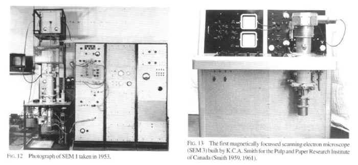
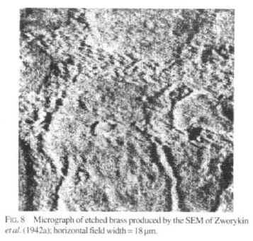
9 Scanning Electron Microscope (SEM) In 1937, Manfred von Ardenne developed a scanning electron microscope : * ** SEM image of etched brass : Early SEM Images *


 STEM Annular bright")


10 Scanning Transmission Electron Microscope (STEM) By scanning electron-beam, TEM resolution can be improved significantly : 0.8 Å resolution York JEOL Nanocentre By STEM, H atoms were directly observed : Capability of STEM Annular dark field (ADF) STEM Annular bright field (ABF) STEM Incident e-beam Specimen Diffraction electrons Detector Collection of electrons with large scattering angles. Collection of electrons with small scattering angles. Observation of heavy atoms. Observation of heavy and light atoms at the same time. * S. D. Findlay et al., Appl. Phys. Exp. 3, (2010).


11 Surface Spectroscopy By introducing electron-beam onto a sample surface : Reflected electron-beam Photo-emission electrons Incident electron-beam Characteristic X-ray Secondary electrons Auger electrons (AES) Sample Auger electrons are found by Lise Meitner in 1922 and Pierre V. Auger in 1925 : * ** Auger Electron Spectroscopy (AES) Penetration depth : * AES signal : Co 2 CrAl Al Cr Co AES mapping : ** * **
12 Electron Probe Micro-Analyser (EPMA) Electron Probe Micro-Analyser (EPMA) : Reflected electron-beam Photo-emission electrons Incident electron-beam Characteristic X-ray (EPMA, EDX) Secondary electrons Incident electron beam Auger electrons Bent crystal Sample Typical penetration depth : ~ 1 µm Detector Wavelength dispersive X-ray spectrometer (WDS) (EPMA) Counter Roland circle Energy dispersive X-ray spectrometer (EDS) (EDX) Example of Co 2 TiSn : EPMA Signals

![patterns Unit cell [110] Real space : fcc (001) surface 2nd 12 02 12 1st 11 01 11 10 00 10 [110] 0th Reciprocal lattice](/docs-images/90/101996502/images/13-1.jpg ": bcc (001) RHEED Observation RHEED patterns of Co 2 FeAl grown on GaAs (001) : [110] Co 2 FeAl 1.")
![0 nm (2 4) GaAs (001) a top view (001) side view [110] Ga [110] 1 As [1-10] [100] Ö 2 Zinc blende a = 0.56533 nm 2.](/docs-images/90/101996502/images/13-2.jpg "0 nm bcc [110] B2 Ö 2 1 7.")
13 Surface Structural Analysis Reflection high energy electron diffraction (RHEED) : Direct spot Shadow edge Sample Screen Typical penetration depth : a few nm Shadow edge [110] [010] [110] Laue spots Clean surface : Streak patterns Unit cell [110] Real space : fcc (001) surface 2nd st [110] 0th Reciprocal lattice : bcc (001) RHEED Observation RHEED patterns of Co 2 FeAl grown on GaAs (001) : [110] Co 2 FeAl 1.0 nm (2 4) GaAs (001) a top view (001) side view [110] Ga [110] 1 As [1-10] [100] Ö 2 Zinc blende a = nm 2.0 nm bcc [110] B2 Ö nm bcc [110] L nm Cr or Fe Al Co c (2 4) unit mesh epitaxial L2 1 (clean surface) Co 2 FeAl (001) <110> GaAs (001) <110>
 Auger electrons Auger diffraction (~ a few atoms) Electron probe microanalyzer (EPMA) Characteristic X-ray Qualitative analysis (sensitivity ~")
14 Major techniques for surface analysis : Surface Analysis Techniques Incident beam Signals Composition Structure Electronic state Auger electron spectroscopy (AES) Auger electrons Qualitative analysis Auger electron spectra Auger electron diffraction (AED) Auger electrons Auger diffraction (~ a few atoms) Electron probe microanalyzer (EPMA) Characteristic X-ray Qualitative analysis (sensitivity ~ 0.1 %) X-ray spectra Energy dispersive X-ray analysis (EDX) Characteristic X-ray Qualitative analysis X-ray spectra X-ray photoelectron spectroscopy (XPS) Photo-emission electrons Qualitative analysis Atomic binding energy Photoemission electron microscopy (PEEM) X-ray / photon Photo-emission electrons Atom mapping Atomic binding energy Secondary ion mass spectroscopy (SIMS) Secondary electrons Qualitative analysis Electron energy-loss spectroscopy (EELS) Reflection high energy diffraction (RHEED) Low energy electron diffraction (LEED) X-ray absorption fine structure (XAFS) X-ray Secondary electrons Reflected electron-beam Reflected electron-beam Photo-emission electrons Surface absorption spectra Surface absorption spectra Reflected diffraction patterns Back-scattered diffraction patterns X-ray diffraction (XRD) X-ray Reflected X-ay X-ray diffraction Transmission electron diffraction (TED) Transmission electrons Diffraction patterns (t < 30 nm) * D. P. Woodruff and T. A. Delchar, Modern Techniques of Surface Science (Cambridge University Press, Cambridge, 1994). Detection Limits of Surface Analysis *
MSE 321 Structural Characterization
 Auger Spectroscopy Auger Electron Spectroscopy (AES) Scanning Auger Microscopy (SAM) Incident Electron Ejected Electron Auger Electron Initial State Intermediate State Final State Physical Electronics
MSE 321 Structural Characterization
 Auger Spectroscopy Auger Electron Spectroscopy (AES) Scanning Auger Microscopy (SAM) Incident Electron Ejected Electron Auger Electron Initial State Intermediate State Final State Physical Electronics
CHARACTERIZATION of NANOMATERIALS KHP
 CHARACTERIZATION of NANOMATERIALS Overview of the most common nanocharacterization techniques MAIN CHARACTERIZATION TECHNIQUES: 1.Transmission Electron Microscope (TEM) 2. Scanning Electron Microscope
MODERN TECHNIQUES OF SURFACE SCIENCE
 MODERN TECHNIQUES OF SURFACE SCIENCE Second edition D. P. WOODRUFF & T. A. DELCHAR Department ofphysics, University of Warwick CAMBRIDGE UNIVERSITY PRESS Contents Preface to first edition Preface to second
Ecole Franco-Roumaine : Magnétisme des systèmes nanoscopiques et structures hybrides - Brasov, Modern Analytical Microscopic Tools
 1. Introduction Solid Surfaces Analysis Group, Institute of Physics, Chemnitz University of Technology, Germany 2. Limitations of Conventional Optical Microscopy 3. Electron Microscopies Transmission Electron
MS482 Materials Characterization ( 재료분석 ) Lecture Note 11: Scanning Probe Microscopy. Byungha Shin Dept. of MSE, KAIST
 Lecture Note 11: Scanning Probe Microscopy. Byungha Shin Dept. of MSE, KAIST") 2015 Fall Semester MS482 Materials Characterization ( 재료분석 ) Lecture Note 11: Scanning Probe Microscopy Byungha Shin Dept. of MSE, KAIST 1 Course Information Syllabus 1. Overview of various characterization
2015 Fall Semester MS482 Materials Characterization ( 재료분석 ) Lecture Note 11: Scanning Probe Microscopy Byungha Shin Dept. of MSE, KAIST 1 Course Information Syllabus 1. Overview of various characterization
Chapter 9. Electron mean free path Microscopy principles of SEM, TEM, LEEM
 Chapter 9 Electron mean free path Microscopy principles of SEM, TEM, LEEM 9.1 Electron Mean Free Path 9. Scanning Electron Microscopy (SEM) -SEM design; Secondary electron imaging; Backscattered electron
AP5301/ Name the major parts of an optical microscope and state their functions.
 Review Problems on Optical Microscopy AP5301/8301-2015 1. Name the major parts of an optical microscope and state their functions. 2. Compare the focal lengths of two glass converging lenses, one with
Structure analysis: Electron diffraction LEED TEM RHEED
 Structure analysis: Electron diffraction LEED: Low Energy Electron Diffraction SPA-LEED: Spot Profile Analysis Low Energy Electron diffraction RHEED: Reflection High Energy Electron Diffraction TEM: Transmission
Nanoelectronics 08. Atsufumi Hirohata Department of Electronics. Quick Review over the Last Lecture E = 2m 0 a 2 ξ 2.
 Nanoelectronics 08 Atsufumi Hirohata Department of Electronics 09:00 Tuesday, 6/February/2018 (P/T 005) Quick Review over the Last Lecture 1D quantum well : E = 2 2m 0 a 2 ξ 2 ( Discrete states ) Quantum
Surface Sensitivity & Surface Specificity
 Surface Sensitivity & Surface Specificity The problems of sensitivity and detection limits are common to all forms of spectroscopy. In its simplest form, the question of sensitivity boils down to whether
Surface Studies by Scanning Tunneling Microscopy
 Surface Studies by Scanning Tunneling Microscopy G. Binnig, H. Rohrer, Ch. Gerber, and E. Weibel IBM Zurich Research Laboratory, 8803 Ruschlikon-ZH, Switzerland (Received by Phys. Rev. Lett. on 30th April,
PHYS-E0541:Special Course in Physics Gas phase synthesis of carbon nanotubes for thin film application. Electron Microscopy. for
 PHYS-E0541:Special Course in Physics Gas phase synthesis of carbon nanotubes for thin film application Electron Microscopy for Introduction to Electron Microscopy Carbon Nanomaterials (nanotubes) Dr. Hua
Film Characterization Tutorial G.J. Mankey, 01/23/04. Center for Materials for Information Technology an NSF Materials Science and Engineering Center
 Film Characterization Tutorial G.J. Mankey, 01/23/04 Theory vs. Experiment A theory is something nobody believes, except the person who made it. An experiment is something everybody believes, except the
Experimental techniques in superatomic physics IV
 Experimental techniques in superatomic physics IV Today Ion scattering Diffraction of x-rays, electrons, and neutrons Transmission and scanning electron microscopies Scanning tunnelling microscopy Atomic
Scanning Probe Microscopy. EMSE-515 F. Ernst
 Scanning Probe Microscopy EMSE-515 F. Ernst 1 Literature 2 3 Scanning Probe Microscopy: The Lab on a Tip by Ernst Meyer,Ans Josef Hug,Roland Bennewitz 4 Scanning Probe Microscopy and Spectroscopy : Theory,
From nanophysics research labs to cell phones. Dr. András Halbritter Department of Physics associate professor
 From nanophysics research labs to cell phones Dr. András Halbritter Department of Physics associate professor Curriculum Vitae Birth: 1976. High-school graduation: 1994. Master degree: 1999. PhD: 2003.
Methods of surface analysis
 Methods of surface analysis Nanomaterials characterisation I RNDr. Věra Vodičková, PhD. Surface of solid matter: last monoatomic layer + absorbed monolayer physical properties are effected (crystal lattice
MS482 Materials Characterization ( 재료분석 ) Lecture Note 2: UPS
 Lecture Note 2: UPS") 2016 Fall Semester MS482 Materials Characterization ( 재료분석 ) Lecture Note 2: UPS Byungha Shin Dept. of MSE, KAIST 1 Course Information Syllabus 1. Overview of various characterization techniques (1 lecture)
2016 Fall Semester MS482 Materials Characterization ( 재료분석 ) Lecture Note 2: UPS Byungha Shin Dept. of MSE, KAIST 1 Course Information Syllabus 1. Overview of various characterization techniques (1 lecture)
Chemical Analysis in TEM: XEDS, EELS and EFTEM. HRTEM PhD course Lecture 5
 Chemical Analysis in TEM: XEDS, EELS and EFTEM HRTEM PhD course Lecture 5 1 Part IV Subject Chapter Prio x-ray spectrometry 32 1 Spectra and mapping 33 2 Qualitative XEDS 34 1 Quantitative XEDS 35.1-35.4
Chapter 10. Nanometrology. Oxford University Press All rights reserved.
 Chapter 10 Nanometrology Oxford University Press 2013. All rights reserved. 1 Introduction Nanometrology is the science of measurement at the nanoscale level. Figure illustrates where nanoscale stands
MS482 Materials Characterization ( 재료분석 ) Lecture Note 4: XRF
 Lecture Note 4: XRF") 2016 Fall Semester MS482 Materials Characterization ( 재료분석 ) Lecture Note 4: XRF Byungha Shin Dept. of MSE, KAIST 1 Course Information Syllabus 1. Overview of various characterization techniques (1 lecture)
2016 Fall Semester MS482 Materials Characterization ( 재료분석 ) Lecture Note 4: XRF Byungha Shin Dept. of MSE, KAIST 1 Course Information Syllabus 1. Overview of various characterization techniques (1 lecture)
MS482 Materials Characterization ( 재료분석 ) Lecture Note 5: RBS
 Lecture Note 5: RBS") 2016 Fall Semester MS482 Materials Characterization ( 재료분석 ) Lecture Note 5: RBS Byungha Shin Dept. of MSE, KAIST 1 Course Information Syllabus 1. Overview of various characterization techniques (1 lecture)
2016 Fall Semester MS482 Materials Characterization ( 재료분석 ) Lecture Note 5: RBS Byungha Shin Dept. of MSE, KAIST 1 Course Information Syllabus 1. Overview of various characterization techniques (1 lecture)
Nanotechnology Nanofabrication of Functional Materials. Marin Alexe Max Planck Institute of Microstructure Physics, Halle - Germany
 Nanotechnology Nanofabrication of Functional Materials Marin Alexe Max Planck Institute of Microstructure Physics, Halle - Germany Contents Part I History and background to nanotechnology Nanoworld Nanoelectronics
Scanning Probe Microscopy (SPM)
") http://ww2.sljus.lu.se/staff/rainer/spm.htm Scanning Probe Microscopy (FYST42 / FAFN30) Scanning Probe Microscopy (SPM) overview & general principles March 23 th, 2018 Jan Knudsen, room K522, jan.knudsen@sljus.lu.se
http://ww2.sljus.lu.se/staff/rainer/spm.htm Scanning Probe Microscopy (FYST42 / FAFN30) Scanning Probe Microscopy (SPM) overview & general principles March 23 th, 2018 Jan Knudsen, room K522, jan.knudsen@sljus.lu.se
Praktikum zur. Materialanalytik
 Praktikum zur Materialanalytik Energy Dispersive X-ray Spectroscopy B513 Stand: 19.10.2016 Contents 1 Introduction... 2 2. Fundamental Physics and Notation... 3 2.1. Alignments of the microscope... 3 2.2.
Lecture 5: Characterization methods
 Lecture 5: Characterization methods X-Ray techniques Single crystal X-Ray Diffration (XRD) Powder XRD Thin film X-Ray Reflection (XRR) Microscopic methods Optical microscopy Electron microscopies (SEM,
Spectroscopies for Unoccupied States = Electrons
 Spectroscopies for Unoccupied States = Electrons Photoemission 1 Hole Inverse Photoemission 1 Electron Tunneling Spectroscopy 1 Electron/Hole Emission 1 Hole Absorption Will be discussed with core levels
Fundamentals of Nanoscale Film Analysis
 Fundamentals of Nanoscale Film Analysis Terry L. Alford Arizona State University Tempe, AZ, USA Leonard C. Feldman Vanderbilt University Nashville, TN, USA James W. Mayer Arizona State University Tempe,
Scanning Electron Microscopy & Ancillary Techniques
 Scanning Electron Microscopy & Ancillary Techniques By Pablo G. Caceres-Valencia The prototype of the first Stereoscan supplied by the Cambridge Instrument Company to the dupont Company, U.S.A. (1965)
MS482 Materials Characterization ( 재료분석 ) Lecture Note 5: RBS. Byungha Shin Dept. of MSE, KAIST
 Lecture Note 5: RBS. Byungha Shin Dept. of MSE, KAIST") 2015 Fall Semester MS482 Materials Characterization ( 재료분석 ) Lecture Note 5: RBS Byungha Shin Dept. of MSE, KAIST 1 Course Information Syllabus 1. Overview of various characterization techniques (1 lecture)
2015 Fall Semester MS482 Materials Characterization ( 재료분석 ) Lecture Note 5: RBS Byungha Shin Dept. of MSE, KAIST 1 Course Information Syllabus 1. Overview of various characterization techniques (1 lecture)
Transmission Electron Microscopy
 L. Reimer H. Kohl Transmission Electron Microscopy Physics of Image Formation Fifth Edition el Springer Contents 1 Introduction... 1 1.1 Transmission Electron Microscopy... 1 1.1.1 Conventional Transmission
Techniques EDX, EELS et HAADF en TEM: possibilités d analyse et applications
 Techniques EDX, EELS et HAADF en TEM: possibilités d analyse et applications Thomas Neisius Université Paul Cézanne Plan Imaging modes HAADF Example: supported Pt nanoparticles Electron sample interaction
Analytical Methods for Materials
 Analytical Methods for Materials Lesson 21 Electron Microscopy and X-ray Spectroscopy Suggested Reading Leng, Chapter 3, pp. 83-126; Chapter 4, pp. 127-160; Chapter 6, pp. 191-219 P.J. Goodhew, J. Humphreys
Scanning Tunneling Microscopy Transmission Electron Microscopy
 Scanning Tunneling Microscopy Transmission Electron Microscopy Speakers Burcu Başar Semih Gezgin Yavuz Selim Telis Place Hacettepe University Department of Chemical Engineering It s a small world after
Solid Surfaces, Interfaces and Thin Films
 Hans Lüth Solid Surfaces, Interfaces and Thin Films Fifth Edition With 427 Figures.2e Springer Contents 1 Surface and Interface Physics: Its Definition and Importance... 1 Panel I: Ultrahigh Vacuum (UHV)
Electron Microscopy I
 Characterization of Catalysts and Surfaces Characterization Techniques in Heterogeneous Catalysis Electron Microscopy I Introduction Properties of electrons Electron-matter interactions and their applications
Lecture 5. X-ray Photoemission Spectroscopy (XPS)
") Lecture 5 X-ray Photoemission Spectroscopy (XPS) 5. Photoemission Spectroscopy (XPS) 5. Principles 5.2 Interpretation 5.3 Instrumentation 5.4 XPS vs UV Photoelectron Spectroscopy (UPS) 5.5 Auger Electron
Lecture 5 X-ray Photoemission Spectroscopy (XPS) 5. Photoemission Spectroscopy (XPS) 5. Principles 5.2 Interpretation 5.3 Instrumentation 5.4 XPS vs UV Photoelectron Spectroscopy (UPS) 5.5 Auger Electron
Chapter 12. Nanometrology. Oxford University Press All rights reserved.
 Chapter 12 Nanometrology Introduction Nanometrology is the science of measurement at the nanoscale level. Figure illustrates where nanoscale stands in relation to a meter and sub divisions of meter. Nanometrology
EDS User School. Principles of Electron Beam Microanalysis
 EDS User School Principles of Electron Beam Microanalysis Outline 1.) Beam-specimen interactions 2.) EDS spectra: Origin of Bremsstrahlung and characteristic peaks 3.) Moseley s law 4.) Characteristic
Surface Analysis - The Principal Techniques
 Surface Analysis - The Principal Techniques Edited by John C. Vickerman Surface Analysis Research Centre, Department of Chemistry UMIST, Manchester, UK JOHN WILEY & SONS Chichester New York Weinheim Brisbane
Spectroscopy at nanometer scale
 Spectroscopy at nanometer scale 1. Physics of the spectroscopies 2. Spectroscopies for the bulk materials 3. Experimental setups for the spectroscopies 4. Physics and Chemistry of nanomaterials Various
Currently, worldwide major semiconductor alloy epitaxial growth is divided into two material groups.
 ICQNM 2014 Currently, worldwide major semiconductor alloy epitaxial growth is divided into two material groups. Cubic: Diamond structures: group IV semiconductors (Si, Ge, C), Cubic zinc-blende structures:
6. Analytical Electron Microscopy
 Physical Principles of Electron Microscopy 6. Analytical Electron Microscopy Ray Egerton University of Alberta and National Institute of Nanotechnology Edmonton, Canada www.tem-eels.ca regerton@ualberta.ca
Quantum Condensed Matter Physics Lecture 12
 Quantum Condensed Matter Physics Lecture 12 David Ritchie QCMP Lent/Easter 2016 http://www.sp.phy.cam.ac.uk/drp2/home 12.1 QCMP Course Contents 1. Classical models for electrons in solids 2. Sommerfeld
Imaging Methods: Scanning Force Microscopy (SFM / AFM)
") Imaging Methods: Scanning Force Microscopy (SFM / AFM) The atomic force microscope (AFM) probes the surface of a sample with a sharp tip, a couple of microns long and often less than 100 Å in diameter.
Imaging Methods: Scanning Force Microscopy (SFM / AFM) The atomic force microscope (AFM) probes the surface of a sample with a sharp tip, a couple of microns long and often less than 100 Å in diameter.
a b c Supplementary Figure S1
 a b c Supplementary Figure S1 AFM measurements of MoS 2 nanosheets prepared from the electrochemical Liintercalation and exfoliation. (a) AFM measurement of a typical MoS 2 nanosheet, deposited on Si/SiO
Local Anodic Oxidation of GaAs: A Nanometer-Scale Spectroscopic Study with PEEM
 Local Anodic Oxidation of GaAs: A Nanometer-Scale Spectroscopic Study with PEEM S. Heun, G. Mori, M. Lazzarino, D. Ercolani, G. Biasiol, and L. Sorba Laboratorio TASC-INFM, 34012 Basovizza, Trieste A.
= 6 (1/ nm) So what is probability of finding electron tunneled into a barrier 3 ev high?
 So what is probability of finding electron tunneled into a barrier 3 ev high?") STM STM With a scanning tunneling microscope, images of surfaces with atomic resolution can be readily obtained. An STM uses quantum tunneling of electrons to map the density of electrons on the surface
STM STM With a scanning tunneling microscope, images of surfaces with atomic resolution can be readily obtained. An STM uses quantum tunneling of electrons to map the density of electrons on the surface
Surface Analysis. Dr. Lynn Fuller Dr. Fuller s Webpage:
 ROCHESTER INSTITUTE OF TECHNOLOGY MICROELECTRONIC ENGINEERING Surface Analysis Dr. Lynn Fuller Dr. Fuller s Webpage: http://people.rit.edu/lffeee 82 Lomb Memorial Drive Rochester, NY 14623-5604 Tel (585)
Lecture 12. study surfaces.
 Lecture 12 Solid Surfaces Techniques to Solid Surfaces. Techniques to study surfaces. Solid Surfaces Molecules on surfaces are not mobile (to large extent) Surfaces have a long-range order (crystalline)
Lecture 23 X-Ray & UV Techniques
 Lecture 23 X-Ray & UV Techniques Schroder: Chapter 11.3 1/50 Announcements Homework 6/6: Will be online on later today. Due Wednesday June 6th at 10:00am. I will return it at the final exam (14 th June).
Nanoelectronics 14. [( ) k B T ] 1. Atsufumi Hirohata Department of Electronics. Quick Review over the Last Lecture.
![Nanoelectronics 14. [( ) k B T ] 1. Atsufumi Hirohata Department of Electronics. Quick Review over the Last Lecture.](/thumbs/85/92941616.jpg "Nanoelectronics 14. [( ) k B T ] 1. Atsufumi Hirohata Department of Electronics. Quick Review over the Last Lecture.") Nanoelectronics 14 Atsufumi Hirohata Department of Electronics 09:00 Tuesday, 27/February/2018 (P/T 005) Quick Review over the Last Lecture Function Fermi-Dirac distribution f ( E) = 1 exp E µ [( ) k B
Nanoelectronics 14 Atsufumi Hirohata Department of Electronics 09:00 Tuesday, 27/February/2018 (P/T 005) Quick Review over the Last Lecture Function Fermi-Dirac distribution f ( E) = 1 exp E µ [( ) k B
Preamble: Emphasis: Material = Device? MTSE 719 PHYSICAL PRINCIPLES OF CHARACTERIZATION OF SOLIDS
 MTSE 719 PHYSICAL PRINCIPLES OF CHARACTERIZATION OF SOLIDS MTSE 719 - PHYSCL PRIN CHARACTIZTN SOLIDS Section # Call # Days / Times 001 96175 -View Book Info - F:100PM - 355PM - TIER114 Preamble: Core course
Experimental methods in physics. Local probe microscopies I
 Experimental methods in physics Local probe microscopies I Scanning tunnelling microscopy (STM) Jean-Marc Bonard Academic year 09-10 1. Scanning Tunneling Microscopy 1.1. Introduction Image of surface
Scanning Tunneling Microscopy. how does STM work? the quantum mechanical picture example of images how can we understand what we see?
 Scanning Tunneling Microscopy how does STM work? the quantum mechanical picture example of images how can we understand what we see? Observation of adatom diffusion with a field ion microscope Scanning
Contrasted strengths and weakness of EDS, WDS and AES for determining the composition of samples
 Contrasted strengths and weakness of EDS, WDS and AES for determining the composition of samples Ana-Marija Nedić Course 590B 12/07/2018 Iowa State University Contrasted strengths and weakness of EDS,
Lecture 4 Scanning Probe Microscopy (SPM)
") Lecture 4 Scanning Probe Microscopy (SPM) General components of SPM; Tip --- the probe; Cantilever --- the indicator of the tip; Tip-sample interaction --- the feedback system; Scanner --- piezoelectric
Lecture 4 Scanning Probe Microscopy (SPM) General components of SPM; Tip --- the probe; Cantilever --- the indicator of the tip; Tip-sample interaction --- the feedback system; Scanner --- piezoelectric
MS482 Materials Characterization ( 재료분석 ) Lecture Note 12: Summary. Byungha Shin Dept. of MSE, KAIST
 Lecture Note 12: Summary. Byungha Shin Dept. of MSE, KAIST") 2015 Fall Semester MS482 Materials Characterization ( 재료분석 ) Lecture Note 12: Summary Byungha Shin Dept. of MSE, KAIST 1 Course Information Syllabus 1. Overview of various characterization techniques (1
2015 Fall Semester MS482 Materials Characterization ( 재료분석 ) Lecture Note 12: Summary Byungha Shin Dept. of MSE, KAIST 1 Course Information Syllabus 1. Overview of various characterization techniques (1
Introduction to Scanning Probe Microscopy Zhe Fei
 Introduction to Scanning Probe Microscopy Zhe Fei Phys 590B, Apr. 2019 1 Outline Part 1 SPM Overview Part 2 Scanning tunneling microscopy Part 3 Atomic force microscopy Part 4 Electric & Magnetic force
Massachusetts Institute of Technology. Dr. Nilanjan Chatterjee
 Massachusetts Institute of Technology Dr. Nilanjan Chatterjee Electron Probe Micro-Analysis (EPMA) Imaging and micrometer-scale chemical compositional analysis of solids Signals produced in The Electron
Nanomaterials and their Optical Applications
 Nanomaterials and their Optical Applications Winter Semester 2012 Lecture 04 rachel.grange@uni-jena.de http://www.iap.uni-jena.de/multiphoton Lecture 4: outline 2 Characterization of nanomaterials SEM,
ABNORMAL X-RAY EMISSION FROM INSULATORS BOMBARDED WITH LOW ENERGY IONS
 302 ABNORMAL X-RAY EMISSION FROM INSULATORS BOMBARDED WITH LOW ENERGY IONS M. Song 1, K. Mitsuishi 1, M. Takeguchi 1, K. Furuya 1, R. C. Birtcher 2 1 High Voltage Electron Microscopy Station, National
Spectroscopy of Nanostructures. Angle-resolved Photoemission (ARPES, UPS)
") Spectroscopy of Nanostructures Angle-resolved Photoemission (ARPES, UPS) Measures all quantum numbers of an electron in a solid. E, k x,y, z, point group, spin E kin, ϑ,ϕ, hν, polarization, spin Electron
Spectroscopy of Nanostructures Angle-resolved Photoemission (ARPES, UPS) Measures all quantum numbers of an electron in a solid. E, k x,y, z, point group, spin E kin, ϑ,ϕ, hν, polarization, spin Electron
Energy Spectroscopy. Ex.: Fe/MgO
 Energy Spectroscopy Spectroscopy gives access to the electronic properties (and thus chemistry, magnetism,..) of the investigated system with thickness dependence Ex.: Fe/MgO Fe O Mg Control of the oxidation
General concept and defining characteristics of AFM. Dina Kudasheva Advisor: Prof. Mary K. Cowman
 General concept and defining characteristics of AFM Dina Kudasheva Advisor: Prof. Mary K. Cowman Overview Introduction History of the SPM invention Technical Capabilities Principles of operation Examples
Compositional mapping of semiconductor quantum dots by X-ray photoemission electron microscopy
 Compositional mapping of semiconductor quantum dots by X-ray photoemission electron microscopy Stefan Heun CNR-INFM, Italy, Laboratorio Nazionale TASC, Trieste and NEST-SNS, Pisa Outline A brief introduction
EE 527 MICROFABRICATION. Lecture 5 Tai-Chang Chen University of Washington
 EE 527 MICROFABRICATION Lecture 5 Tai-Chang Chen University of Washington MICROSCOPY AND VISUALIZATION Electron microscope, transmission electron microscope Resolution: atomic imaging Use: lattice spacing.
The Use of Synchrotron Radiation in Modern Research
 The Use of Synchrotron Radiation in Modern Research Physics Chemistry Structural Biology Materials Science Geochemical and Environmental Science Atoms, molecules, liquids, solids. Electronic and geometric
Chemical characterization of semiconductor nanostructures by energy filtered PEEM
 Chemical characterization of semiconductor nanostructures by energy filtered PEEM S. Heun TASC-INFM Laboratory, Area di Ricerca di Trieste, Basovizza, SS-14, Km 163.5, 34012 Trieste, ITALY Outline A brief
Gaetano L Episcopo. Scanning Electron Microscopy Focus Ion Beam and. Pulsed Plasma Deposition
 Gaetano L Episcopo Scanning Electron Microscopy Focus Ion Beam and Pulsed Plasma Deposition Hystorical background Scientific discoveries 1897: J. Thomson discovers the electron. 1924: L. de Broglie propose
Nanoscale Surface Physics PHY 5XXX
 SYLLABUS Nanoscale Surface Physics PHY 5XXX Spring Semester, 2006 Instructor: Dr. Beatriz Roldán-Cuenya Time: Tuesday and Thursday 4:00 to 5:45 pm Location: Theory: MAP 306, Laboratory: MAP 148 Office
Energy Spectroscopy. Excitation by means of a probe
 Energy Spectroscopy Excitation by means of a probe Energy spectral analysis of the in coming particles -> XAS or Energy spectral analysis of the out coming particles Different probes are possible: Auger
STM spectroscopy (STS)
") STM spectroscopy (STS) di dv 4 e ( E ev, r) ( E ) M S F T F Basic concepts of STS. With the feedback circuit open the variation of the tunneling current due to the application of a small oscillating voltage
STM spectroscopy (STS) di dv 4 e ( E ev, r) ( E ) M S F T F Basic concepts of STS. With the feedback circuit open the variation of the tunneling current due to the application of a small oscillating voltage
Nanoelectronics 12. Atsufumi Hirohata Department of Electronics. Quick Review over the Last Lecture
 Nanoelectronics 12 Atsufumi Hirohata Department of Electronics 09:00 Tuesday, 20/February/2018 (P/T 005) Quick Review over the Last Lecture Origin of magnetism : ( Circular current ) is equivalent to a
MT Electron microscopy Scanning electron microscopy and electron probe microanalysis
 MT-0.6026 Electron microscopy Scanning electron microscopy and electron probe microanalysis Eero Haimi Research Manager Outline 1. Introduction Basics of scanning electron microscopy (SEM) and electron
Scanning Tunneling Microscopy
 Scanning Tunneling Microscopy References: 1. G. Binnig, H. Rohrer, C. Gerber, and Weibel, Phys. Rev. Lett. 49, 57 (1982); and ibid 50, 120 (1983). 2. J. Chen, Introduction to Scanning Tunneling Microscopy,
Scanning Probe Microscopy. Amanda MacMillan, Emmy Gebremichael, & John Shamblin Chem 243: Instrumental Analysis Dr. Robert Corn March 10, 2010
 Scanning Probe Microscopy Amanda MacMillan, Emmy Gebremichael, & John Shamblin Chem 243: Instrumental Analysis Dr. Robert Corn March 10, 2010 Scanning Probe Microscopy High-Resolution Surface Analysis
tip conducting surface
 PhysicsAndMathsTutor.com 1 1. The diagram shows the tip of a scanning tunnelling microscope (STM) above a conducting surface. The tip is at a potential of 1.0 V relative to the surface. If the tip is sufficiently
An Introduction to Auger Electron Spectroscopy
 An Introduction to Auger Electron Spectroscopy Spyros Diplas MENA3100 SINTEF Materials & Chemistry, Department of Materials Physics & Centre of Materials Science and Nanotechnology, Department of Chemistry,
Recommendations for abbreviations in surface science and chemical spectroscopy. (1) The electron, photoelectron and related spectroscopies
 The electron, photoelectron and related spectroscopies") 17.6.3 Recommendations for abbreviations in surface science and chemical spectroscopy The overall list of selected techniques and their abbreviations have been subdivided under the following principal
17.6.3 Recommendations for abbreviations in surface science and chemical spectroscopy The overall list of selected techniques and their abbreviations have been subdivided under the following principal
Photoemission Electron Microscopy (PEEM)
") PHOTOEMISSION ELECTRON MICROSCOPY Pat Photongkam Research Facility Division Synchrotron Light Research Institute (Public Organization) Synchrotron Light Research Institute (Public Organization) 111 University
PHOTOEMISSION ELECTRON MICROSCOPY Pat Photongkam Research Facility Division Synchrotron Light Research Institute (Public Organization) Synchrotron Light Research Institute (Public Organization) 111 University
Department of Electrical Engineering and Information Systems, Tanaka-Ohya lab.
 Observation of the room-temperature local ferromagnetism and its nanoscale expansion in the ferromagnetic semiconductor Ge 1 xfe x Yuki K. Wakabayashi 1 and Yukio Takahashi 2 1 Department of Electrical
Electron Microprobe Analysis and Scanning Electron Microscopy
 Electron Microprobe Analysis and Scanning Electron Microscopy Electron microprobe analysis (EMPA) Analytical technique in which a beam of electrons is focused on a sample surface, producing X-rays from
IMAGING DIFFRACTION SPECTROSCOPY
 TEM Techniques TEM/STEM IMAGING DIFFRACTION SPECTROSCOPY Amplitude contrast (diffracion contrast) Phase contrast (highresolution imaging) Selected area diffraction Energy dispersive X-ray spectroscopy
Studying Metal to Insulator Transitions in Solids using Synchrotron Radiation-based Spectroscopies.
 PY482 Lecture. February 28 th, 2013 Studying Metal to Insulator Transitions in Solids using Synchrotron Radiation-based Spectroscopies. Kevin E. Smith Department of Physics Department of Chemistry Division
Nanoelectronics 04. Atsufumi Hirohata Department of Electronics. Quick Review over the Last Lecture ' E = A. ' t gradφ ' ) / ' ) ε ρ
 / ' ) ε ρ") Nanoelectronics 04 Atsufumi Hirohata Department of Electronics 09:00 Tuesday, 23/January/2018 (P/T 005) Quick Review over the Last Lecture Maxwell equations with ( scalar ) potential ( f ) and ( vector
Nanoelectronics 04 Atsufumi Hirohata Department of Electronics 09:00 Tuesday, 23/January/2018 (P/T 005) Quick Review over the Last Lecture Maxwell equations with ( scalar ) potential ( f ) and ( vector
Microscopical and Microanalytical Methods (NANO3)
") Microscopical and Microanalytical Methods (NANO3) 06.11.15 10:15-12:00 Introduction - SPM methods 13.11.15 10:15-12:00 STM 20.11.15 10:15-12:00 STS Erik Zupanič erik.zupanic@ijs.si stm.ijs.si 27.11.15
Microscopical and Microanalytical Methods (NANO3) 06.11.15 10:15-12:00 Introduction - SPM methods 13.11.15 10:15-12:00 STM 20.11.15 10:15-12:00 STS Erik Zupanič erik.zupanic@ijs.si stm.ijs.si 27.11.15
Name: (a) What core levels are responsible for the three photoelectron peaks in Fig. 1?
 What core levels are responsible for the three photoelectron peaks in Fig. 1?") Physics 243A--Surface Physics of Materials: Spectroscopy Final Examination December 16, 2014 (3 problems, 100 points total, open book, open notes and handouts) Name: [1] (50 points), including Figures
Physics 243A--Surface Physics of Materials: Spectroscopy Final Examination December 16, 2014 (3 problems, 100 points total, open book, open notes and handouts) Name: [1] (50 points), including Figures
IV. Surface analysis for chemical state, chemical composition
 IV. Surface analysis for chemical state, chemical composition Probe beam Detect XPS Photon (X-ray) Photoelectron(core level electron) UPS Photon (UV) Photoelectron(valence level electron) AES electron
CHEM 681 Seminar Mingqi Zhao April 20, 1998 Room 2104, 4:00 p.m. High Resolution Transmission Electron Microscopy: theories and applications
 CHEM 681 Seminar Mingqi Zhao April 20, 1998 Room 2104, 4:00 p.m. High Resolution Transmission Electron Microscopy: theories and applications In materials science, people are always interested in viewing
Surface Analysis - The Principal Techniques
 Surface Analysis - The Principal Techniques 2nd Edition Editors johnc.vickerman Manchester Interdisciplinary Biocentre, University of Manchester, UK IAN S. GILMORE National Physical Laboratory, Teddington,
And Manipulation by Scanning Probe Microscope
 Basic 15 Nanometer Scale Measurement And Manipulation by Scanning Probe Microscope Prof. K. Fukuzawa Dept. of Micro/Nano Systems Engineering Nagoya University I. Basics of scanning probe microscope Basic
SOLID STATE PHYSICS PHY F341. Dr. Manjuladevi.V Associate Professor Department of Physics BITS Pilani
 SOLID STATE PHYSICS PHY F341 Dr. Manjuladevi.V Associate Professor Department of Physics BITS Pilani 333031 manjula@bits-pilani.ac.in Characterization techniques SEM AFM STM BAM Outline What can we use
8 Summary and outlook
 91 8 Summary and outlook The main task of present work was to investigate the growth, the atomic and the electronic structures of Co oxide as well as Mn oxide films on Ag(001) by means of STM/STS at LT
Concepts in Surface Physics
 M.-C. Desjonqueres D. Spanjaard Concepts in Surface Physics Second Edition With 257 Figures Springer 1. Introduction................................. 1 2. Thermodynamical and Statistical Properties of
High Resolution Photoemission Study of the Spin-Dependent Band Structure of Permalloy and Ni
 High Resolution Photoemission Study of the Spin-Dependent Band Structure of Permalloy and Ni K. N. Altmann, D. Y. Petrovykh, and F. J. Himpsel Department of Physics, University of Wisconsin, Madison, 1150
MICRO-TOMOGRAPHY AND X-RAY ANALYSIS OF GEOLOGICAL SAMPLES
 THE PUBLISHING HOUSE PROCEEDINGS OF THE ROMANIAN ACADEMY, Series A, OF THE ROMANIAN ACADEMY Volume 18, Number 1/2017, pp. 42 49 MICRO-TOMOGRAPHY AND X-RAY ANALYSIS OF GEOLOGICAL SAMPLES Ion GRUIA University
Characterisation of Catalysts Using Secondary and Backscattered Electron In-lens Detectors
 Platinum Metals Rev., 2014, 58, (2), 106 110 FINAL ANALYSIS Characterisation of Catalysts Using Secondary and Backscattered Electron In-lens Detectors Heterogeneous catalysis often involves the use of
Lecture 20 Optical Characterization 2
 Lecture 20 Optical Characterization 2 Schroder: Chapters 2, 7, 10 1/68 Announcements Homework 5/6: Is online now. Due Wednesday May 30th at 10:00am. I will return it the following Wednesday (6 th June).