Structure analysis: Electron diffraction LEED TEM RHEED
|
|
|
- Myles Mitchell
- 5 years ago
- Views:
Transcription
1 Structure analysis: Electron diffraction LEED: Low Energy Electron Diffraction SPA-LEED: Spot Profile Analysis Low Energy Electron diffraction RHEED: Reflection High Energy Electron Diffraction TEM: Transmission Electron Microscopy LEED RHEED TEM k i k i k f k i k f k f E = ev E = kev E = kev Electron mean free path
2 Basic theory of diffraction By the principles of wave-particle duality, the beam of electrons may be equally regarded as a succession of electron waves incident normally on the sample. These waves will be scattered by regions of high localized electron density, i.e. the surface atoms, which can therefore be considered to act as point scatterers. The wavelength of the electrons is given be the de Broglie relation : Wavelength, λ = h / p ( where p - electron momentum ) Now, p = m v = (2 m E ) 1/2 = (2 m e V) 1/2 λ = h / ( 2 m e V ) 1/2 h Planck constant = J s m electron mass = Kg v electron velocity E electron kinetic energy e electron charge = C Example: 1) Electron energy = 20 ev -> Wavelength = 2.7 Å 2) Electron energy = 200 ev -> Wavelength = 0.87 Å λ comparable to the atomic spacing N.B.: Electron energy = 2 ev -> Wavelength = 8.5 Å i.e. the hypothetical RLEED would have low resolution
3 Plane wave scattered by a point f(θ,r) e ir k f e ir k i In the case of many scatter points the scattered wave is given by: Σ j f j (θ,r j ) e ir j k f f j (θ,r j ) is the atomic structure factor
4 Two points scattering n i k i k i = 2πn i /λ n f d cos θ i = d n i θ i d k f = 2πn f /λ θ f d cos θ f = - d n f k f Elastic scattering: k i = k f or the incident and reflected rays have the same wavelength λ Constructive interference: d cos θ i + d cos θ f = d (n i -n f ) = m λ or d (k i -k f ) = 2πm m integral This is also equivalent to: e -id (k i kf) = 1 Bravais lattice The condition of constructive interference has to be verified by all the lattice points, i.e. R (k i -k f ) = 2πm with R Bravais lattice vector, or (k i -k f ) = G with G is a vector of the reciprocal lattice
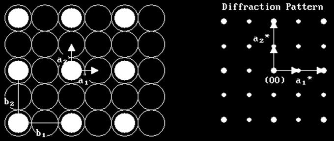
5 Laue s diffraction condition: k f = k i ± G Given an incident wave k i, the diffraction spots are located by the k f vectors verifying: 1) k i = k f 2) k f = k i ± G 2D case or the case of a surface 2D lattice described by R s implying R s (k i -k f ) = 2πm or (k f -k i ) // = Δk // = ± G s with G s vector of the 2D reciprocal lattice The diffraction spots is a map of the 2D reciprocal lattice Example a 1* = 2π/ a 1 a 1 / a 1 a 2 a 2* = 2π/ a 2 a 2 / a 2 a 1 k i =(0,0,1) R s = 1 a a 2 = (a 1, a 2,0) G s = s (1 a 1* + 1 a 2* ) = s (2π/a 1, 2π/a 2,0) k f = (2πs/a 1, 2πs/a 2,c) with c 2 = 1 (2πs/a 1 ) 2 (2πs/a 2 ) 2 k i k f G 1 G 2
 e ir h G = f Σ R")
6 Bravais lattice with basis Consider the elementary cell located at R and assume the cell containing a basis of N atoms. The coordinates of the j-atom in the cell are: r j = R + d j with d j the position vector inside the cell The amplitude of the diffracted wave is given by: Ψ= Σ h all atoms f(r h ) e ir h G = f Σ R Bravais Σ j N e ir j G (f identical for all atoms) In general f is atom dependent -> spot intensity reflects the atomic structure factor Diffraction from N = N 1 x N 2 lattice points 1 + e -iα +.. e -i(n 1-1)α + e -i(n 2-1)α I(G s ) T(G s ) 2 = Π i=12 sin 2 (N i R i G s /2)/ sin 2 (R i G s /2) Peak width inversely proportional to N
7 LEED may be used in one of two ways Qualitatively : the diffraction pattern is recorded; analysis of the spot positions yields information on the size, symmetry and rotational alignment of the surface unit cell with respect to the substrate unit cell. Quantitatively : the intensities of the various diffracted beams are recorded as a function of the incident electron beam energy; comparison with theoretical curves, may provide accurate information on atomic positions. Experimental set-up The LEED experiment uses a beam of electrons of a well-defined low energy incident normally on the sample. Only the elastically-scattered electrons contribute to the diffraction pattern ; the lower energy (secondary) electrons are removed by energy-filtering grids placed in front of the fluorescent screen that is employed to display the pattern.


8 fcc(100) (0,0) represents the reflected beam along the surface normal fcc(110) Real space Diffraction pattern a 2 * a 2 a 1 * a 1 a 1* = 2π/a 1 a 2* = 2π/a 2
 b 2")
")
]")
9 fcc(100) (2x2) b 2 * b 1 * fcc(100) ( 2x 2) R45 [c(2x2)]
10 Fcc(111) + adsorbate a 1s = 2 a a 2 a 2s = -1 a a 2 Ideal surface Real surface Three possible domains rotated by 60 depending on the terrace
11 Spot diffraction due to surface defects I 0 I steps I atoms I down I up

12 LEED is sensible to surface defects Steps behave like 1D adsorbate nets
13 Spot Profile Analysis Ideal case: the diffraction spots are described by δ functions Real case: the diffraction spots are described by Gauss s functions Reasons of the intrinsic width of the diffraction spot: 1) Electron energy non perfectly monochromatic 2) Electron beam non perfectly normal to the sample surface 3) Incident wave non perfectly plane 4) Aberrations of the optics but also The sample surface is not a ideal flat surface steps, islands, adsorbates, etc. The observed spot O(G) is the convolution of the ideal diffraction spot I(G) with the instrumental transfer function T(G) and the surface defect diffraction S(G): O(G) = I(G) * T(G) * S(G) The Fourier transform of T(G) is a gaussian function The HWHM is defined as the transfer width and define the maximum surface distance on which the diffraction is coherent (about nm)
 ion sputtered at room temperature.")

14 SPA-LEED Large transfer width nm STM images of Cu(100) ion sputtered at room temperature. Ion sputtering at normal incidence produces square pits 200 x 200 nm 2 SPA-LEED patterns
 J.")
 Surface")

15 Rusponi et al. Appl. Phys. Lett. 75, 3318 (1999) J. Wollschläger et al., Phys. Rev. B 57, (1998) Surface morphology for different ion sputtering direction STM SPA-LEED 350 x 350 nm 2

 and consequently only the periodicity perpendicularly to the incidence direction is")
16 RHEED Electron penetration depth λ = nm at 40 kev for normal incidence Surface sensibility if cos ϕ = d/λ with d = 1-2 atomic layers or ϕ about 89 Vertical bars in place of spots because due to the geometry the technique is strongly sensible to surface defects (in the impinging direction) Due to the grazing incidence the surface is seen as a continuous along the incidence direction (no diffraction) and consequently only the periodicity perpendicularly to the incidence direction is detected
17 RHEED spectrum e - beam The spectrum is visible only if the incident beam is aligned with a symmetry direction of the substrate
18 RHEED sensibility to surface defects Growth of GaAs(100) by Molecular Beam Epitaxy (MBE) Neave et al. Appl. Phys. A31, 1 (1983) The intensity oscillations are a measure of the surface disorder Oscillation period: 1 atomic layer Intensity: decreasing with the number of deposited layers Imperfect layer by layer growth Maximum disorder at 0.5 ML during layer by layer growth
19 What advantages does RHEED offer over LEED? Pro: 1) The geometry of the experiment allows much better access to the sample during observation of the diffraction pattern. This is particularly important if it is desired to make observations of the surface structure during growth of a surface film by evaporation from sources located normal to the sample surface or simultaneous with other measurements (e.g. AES, XPS). 2) Experiments have shown that it is possible to monitor the atomic layer-by-atomic layer growth of epitaxial films by monitoring oscillations in the intensity of the diffracted beams in the RHEED pattern. Con: 1) quality of the diffraction pattern frequently lower 2) diffraction patterns have to be observed for at least two sample alignments with respect to the incident beam in order to determine the surface unit cell.
20 Transmission Electron Microscope (TEM) Conceptually is identical to an optical microscope where electrons are used in place of photons Diffraction plane photons electrons E = 75 kev -> λ = 0.05 Å Theoretical resolution about hundred thousands times better than that of light.

21 Unfortunately, this theoretical resolution has never come even close to being attained. The basic draw back is that magnetic fields can not be manipulated, shaped and grouped the way an optical engineer does with glass lenses. There are several disadvantages of electron optics. 1)Electrons are easily effected by any mater they encounter. When they do encounter mater the interaction results in the emission of all the lower forms of energy. Such as x-rays, secondary electrons, ultraviolet, heat etc. 2) Complicate to describe the scattering process inside the object 3) The wave function resulting from the scattering process is falsified by the optical system 4)The electrons can not pass through air. As a result the microscope has to be kept in a high vacuum. 5)Our eyes are not sensitive to electrons so the operator must learn to focus the instrument using different focal cues than he is used to. Advantages of TEM over light microscopes: 1) about a thousand fold increase in resolution 2) a hundred fold increase in depth of field. TEM image of DNA
 (Fe(001)) axis and MgO(100) (Fe(110)) axis. Lattice dislocations are circled. The lattice spacing of MgO is 0.")
22 TEM images of a single-crystal MTJ with the Fe(001)/MgO(001)(1.8 nm)/fe(001) structure. b is a magnification of a. The vertical and horizontal directions respectively correspond to the MgO(001) (Fe(001)) axis and MgO(100) (Fe(110)) axis. Lattice dislocations are circled. The lattice spacing of MgO is nm along the [001] axis and nm along the [100] axis. The lattice of the top Fe electrode is slightly expanded along the [110] axis. Nature Materials 3, (2004)
Surface Sensitivity & Surface Specificity
 Surface Sensitivity & Surface Specificity The problems of sensitivity and detection limits are common to all forms of spectroscopy. In its simplest form, the question of sensitivity boils down to whether
Energy Spectroscopy. Excitation by means of a probe
 Energy Spectroscopy Excitation by means of a probe Energy spectral analysis of the in coming particles -> XAS or Energy spectral analysis of the out coming particles Different probes are possible: Auger
Energy Spectroscopy. Ex.: Fe/MgO
 Energy Spectroscopy Spectroscopy gives access to the electronic properties (and thus chemistry, magnetism,..) of the investigated system with thickness dependence Ex.: Fe/MgO Fe O Mg Control of the oxidation
Structure of Surfaces
 Structure of Surfaces C Stepped surface Interference of two waves Bragg s law Path difference = AB+BC =2dsin ( =glancing angle) If, n =2dsin, constructive interference Ex) in a cubic lattice of unit cell
disordered, ordered and coherent with the substrate, and ordered but incoherent with the substrate.
 5. Nomenclature of overlayer structures Thus far, we have been discussing an ideal surface, which is in effect the structure of the topmost substrate layer. The surface (selvedge) layers of the solid however
Imaging Methods: Scanning Force Microscopy (SFM / AFM)
") Imaging Methods: Scanning Force Microscopy (SFM / AFM) The atomic force microscope (AFM) probes the surface of a sample with a sharp tip, a couple of microns long and often less than 100 Å in diameter.
Imaging Methods: Scanning Force Microscopy (SFM / AFM) The atomic force microscope (AFM) probes the surface of a sample with a sharp tip, a couple of microns long and often less than 100 Å in diameter.
MSE 321 Structural Characterization
 Auger Spectroscopy Auger Electron Spectroscopy (AES) Scanning Auger Microscopy (SAM) Incident Electron Ejected Electron Auger Electron Initial State Intermediate State Final State Physical Electronics
M2 TP. Low-Energy Electron Diffraction (LEED)
") M2 TP Low-Energy Electron Diffraction (LEED) Guide for report preparation I. Introduction: Elastic scattering or diffraction of electrons is the standard technique in surface science for obtaining structural
M2 TP Low-Energy Electron Diffraction (LEED) Guide for report preparation I. Introduction: Elastic scattering or diffraction of electrons is the standard technique in surface science for obtaining structural
object objective lens eyepiece lens
 Advancing Physics G495 June 2015 SET #1 ANSWERS Field and Particle Pictures Seeing with electrons The compound optical microscope Q1. Before attempting this question it may be helpful to review ray diagram
Nanoelectronics 09. Atsufumi Hirohata Department of Electronics. Quick Review over the Last Lecture
 Nanoelectronics 09 Atsufumi Hirohata Department of Electronics 13:00 Monday, 12/February/2018 (P/T 006) Quick Review over the Last Lecture ( Field effect transistor (FET) ): ( Drain ) current increases
Chapter 10: Wave Properties of Particles
 Chapter 10: Wave Properties of Particles Particles such as electrons may demonstrate wave properties under certain conditions. The electron microscope uses these properties to produce magnified images
MSE 321 Structural Characterization
 Auger Spectroscopy Auger Electron Spectroscopy (AES) Scanning Auger Microscopy (SAM) Incident Electron Ejected Electron Auger Electron Initial State Intermediate State Final State Physical Electronics
Film Characterization Tutorial G.J. Mankey, 01/23/04. Center for Materials for Information Technology an NSF Materials Science and Engineering Center
 Film Characterization Tutorial G.J. Mankey, 01/23/04 Theory vs. Experiment A theory is something nobody believes, except the person who made it. An experiment is something everybody believes, except the
Quantum Interference and Duality
 Quantum Interference and Duality Kiyohide NOMURA Department of Physics December 21, 2016 1 / 49 Quantum Physics(Mechanics) Basic notion of Quantum Physics: Wave-Particle Duality Light (electromagnetic
2. Diffraction as a means to determine crystal structure
 Page 1 of 22 2. Diffraction as a means to determine crystal structure Recall de Broglie matter waves: 2 p h E = where p = 2m λ h 1 E = ( ) 2m λ hc E = hυ = ( photons) λ ( matter wave) He atoms: [E (ev)]
AP5301/ Name the major parts of an optical microscope and state their functions.
 Review Problems on Optical Microscopy AP5301/8301-2015 1. Name the major parts of an optical microscope and state their functions. 2. Compare the focal lengths of two glass converging lenses, one with
MODERN TECHNIQUES OF SURFACE SCIENCE
 MODERN TECHNIQUES OF SURFACE SCIENCE Second edition D. P. WOODRUFF & T. A. DELCHAR Department ofphysics, University of Warwick CAMBRIDGE UNIVERSITY PRESS Contents Preface to first edition Preface to second
High-Resolution. Transmission. Electron Microscopy
 Part 4 High-Resolution Transmission Electron Microscopy 186 Significance high-resolution transmission electron microscopy (HRTEM): resolve object details smaller than 1nm (10 9 m) image the interior of
= 6 (1/ nm) So what is probability of finding electron tunneled into a barrier 3 ev high?
 So what is probability of finding electron tunneled into a barrier 3 ev high?") STM STM With a scanning tunneling microscope, images of surfaces with atomic resolution can be readily obtained. An STM uses quantum tunneling of electrons to map the density of electrons on the surface
STM STM With a scanning tunneling microscope, images of surfaces with atomic resolution can be readily obtained. An STM uses quantum tunneling of electrons to map the density of electrons on the surface
An Introduction to Diffraction and Scattering. School of Chemistry The University of Sydney
 An Introduction to Diffraction and Scattering Brendan J. Kennedy School of Chemistry The University of Sydney 1) Strong forces 2) Weak forces Types of Forces 3) Electromagnetic forces 4) Gravity Types
2. Diffraction as a means to determine crystal structure
 2. Diffraction as a means to determine crystal structure Recall de Broglie matter waves: He atoms: [E (ev)] 1/2 = 0.14 / (Å) E 1Å = 0.0196 ev Neutrons: [E (ev)] 1/2 = 0.28 / (Å) E 1Å = 0.0784 ev Electrons:
Elastic and Inelastic Scattering in Electron Diffraction and Imaging
 Elastic and Inelastic Scattering in Electron Diffraction and Imaging Contents Introduction Symbols and definitions Part A Diffraction and imaging of elastically scattered electrons Chapter 1. Basic kinematical
tip conducting surface
 PhysicsAndMathsTutor.com 1 1. The diagram shows the tip of a scanning tunnelling microscope (STM) above a conducting surface. The tip is at a potential of 1.0 V relative to the surface. If the tip is sufficiently
4. Other diffraction techniques
 4. Other diffraction techniques 4.1 Reflection High Energy Electron Diffraction (RHEED) Setup: - Grazing-incidence high energy electron beam (3-5 kev: MEED,
Grazing Incidence Fast Atom Diffraction: a new tool for surface characterization
 Grazing Incidence Fast Atom Diffraction: a new tool for surface characterization Victor H. Etgens Institut des NanoSciences de Paris Outline Introduction GIFAD : technique how it works; Experimental set-up;
Transmission Electron Microscopy
 L. Reimer H. Kohl Transmission Electron Microscopy Physics of Image Formation Fifth Edition el Springer Contents 1 Introduction... 1 1.1 Transmission Electron Microscopy... 1 1.1.1 Conventional Transmission
MS482 Materials Characterization ( 재료분석 ) Lecture Note 5: RBS. Byungha Shin Dept. of MSE, KAIST
 Lecture Note 5: RBS. Byungha Shin Dept. of MSE, KAIST") 2015 Fall Semester MS482 Materials Characterization ( 재료분석 ) Lecture Note 5: RBS Byungha Shin Dept. of MSE, KAIST 1 Course Information Syllabus 1. Overview of various characterization techniques (1 lecture)
2015 Fall Semester MS482 Materials Characterization ( 재료분석 ) Lecture Note 5: RBS Byungha Shin Dept. of MSE, KAIST 1 Course Information Syllabus 1. Overview of various characterization techniques (1 lecture)
Lecture 23 X-Ray & UV Techniques
 Lecture 23 X-Ray & UV Techniques Schroder: Chapter 11.3 1/50 Announcements Homework 6/6: Will be online on later today. Due Wednesday June 6th at 10:00am. I will return it at the final exam (14 th June).
CHEM 681 Seminar Mingqi Zhao April 20, 1998 Room 2104, 4:00 p.m. High Resolution Transmission Electron Microscopy: theories and applications
 CHEM 681 Seminar Mingqi Zhao April 20, 1998 Room 2104, 4:00 p.m. High Resolution Transmission Electron Microscopy: theories and applications In materials science, people are always interested in viewing
MS482 Materials Characterization ( 재료분석 ) Lecture Note 5: RBS
 Lecture Note 5: RBS") 2016 Fall Semester MS482 Materials Characterization ( 재료분석 ) Lecture Note 5: RBS Byungha Shin Dept. of MSE, KAIST 1 Course Information Syllabus 1. Overview of various characterization techniques (1 lecture)
2016 Fall Semester MS482 Materials Characterization ( 재료분석 ) Lecture Note 5: RBS Byungha Shin Dept. of MSE, KAIST 1 Course Information Syllabus 1. Overview of various characterization techniques (1 lecture)
Experimental Determination of Crystal Structure
 Experimental Determination of Crystal Structure Branislav K. Nikolić Department of Physics and Astronomy, University of Delaware, U.S.A. PHYS 624: Introduction to Solid State Physics http://www.physics.udel.edu/~bnikolic/teaching/phys624/phys624.html
PROBING CRYSTAL STRUCTURE
 PROBING CRYSTAL STRUCTURE Andrew Baczewski PHY 491, October 10th, 2011 OVERVIEW First - we ll briefly discuss Friday s quiz. Today, we will answer the following questions: How do we experimentally probe
Wafer holders. Mo- or Ta- made holders Bonding: In (Ga), or In-free (clamped) Quick and easy transfer
, or In-free (clamped) Quick and easy transfer") Wafer holders Mo- or Ta- made holders Bonding: In (Ga), or In-free (clamped) Quick and easy transfer Image: In-free, 3-inch sample holder fitting a quarter of a 2- inch wafer Reflection High Energy Electron
Wafer holders Mo- or Ta- made holders Bonding: In (Ga), or In-free (clamped) Quick and easy transfer Image: In-free, 3-inch sample holder fitting a quarter of a 2- inch wafer Reflection High Energy Electron
V 11: Electron Diffraction
 Martin-Luther-University Halle-Wittenberg Institute of Physics Advanced Practical Lab Course V 11: Electron Diffraction An electron beam conditioned by an electron optical system is diffracted by a polycrystalline,
Methods of surface analysis
 Methods of surface analysis Nanomaterials characterisation I RNDr. Věra Vodičková, PhD. Surface of solid matter: last monoatomic layer + absorbed monolayer physical properties are effected (crystal lattice
SOLID STATE 18. Reciprocal Space
 SOLID STATE 8 Reciprocal Space Wave vectors and the concept of K-space can simplify the explanation of several properties of the solid state. They will be introduced to provide more information on diffraction
Lecture 20 Optical Characterization 2
 Lecture 20 Optical Characterization 2 Schroder: Chapters 2, 7, 10 1/68 Announcements Homework 5/6: Is online now. Due Wednesday May 30th at 10:00am. I will return it the following Wednesday (6 th June).
Solid Surfaces, Interfaces and Thin Films
 Hans Lüth Solid Surfaces, Interfaces and Thin Films Fifth Edition With 427 Figures.2e Springer Contents 1 Surface and Interface Physics: Its Definition and Importance... 1 Panel I: Ultrahigh Vacuum (UHV)
STM spectroscopy (STS)
") STM spectroscopy (STS) di dv 4 e ( E ev, r) ( E ) M S F T F Basic concepts of STS. With the feedback circuit open the variation of the tunneling current due to the application of a small oscillating voltage
STM spectroscopy (STS) di dv 4 e ( E ev, r) ( E ) M S F T F Basic concepts of STS. With the feedback circuit open the variation of the tunneling current due to the application of a small oscillating voltage
E. K. A. ADVANCED PHYSICS LABORATORY PHYSICS 3081, 4051
 E. K. A. ADVANCED PHYSICS LABORATORY PHYSICS 38, 45 ELECTRON DIFFRACTION Introduction This experiment, using a cathode ray tube, permits the first hand observation that electrons, which are usually though
MIDTERM 3 REVIEW SESSION. Dr. Flera Rizatdinova
 MIDTERM 3 REVIEW SESSION Dr. Flera Rizatdinova Summary of Chapter 23 Index of refraction: Angle of reflection equals angle of incidence Plane mirror: image is virtual, upright, and the same size as the
Module 02: Wave-particle duality, de Broglie waves and the Uncertainty principle
 PG Pathshala Subject: BIOPHYSICS Paper 0: Quantum Biophysics Module 0: Wave-particle duality, de Broglie waves and the Uncertainty principle Principal Investigator: Prof. Moganty R. Rajeswari Professor,
Experimental methods in physics. Local probe microscopies I
 Experimental methods in physics Local probe microscopies I Scanning tunnelling microscopy (STM) Jean-Marc Bonard Academic year 09-10 1. Scanning Tunneling Microscopy 1.1. Introduction Image of surface
Gaetano L Episcopo. Scanning Electron Microscopy Focus Ion Beam and. Pulsed Plasma Deposition
 Gaetano L Episcopo Scanning Electron Microscopy Focus Ion Beam and Pulsed Plasma Deposition Hystorical background Scientific discoveries 1897: J. Thomson discovers the electron. 1924: L. de Broglie propose
Direct observation of a Ga adlayer on a GaN(0001) surface by LEED Patterson inversion. Xu, SH; Wu, H; Dai, XQ; Lau, WP; Zheng, LX; Xie, MH; Tong, SY
 surface by LEED Patterson inversion. Xu, SH; Wu, H; Dai, XQ; Lau, WP; Zheng, LX; Xie, MH; Tong, SY") Title Direct observation of a Ga adlayer on a GaN(0001) surface by LEED Patterson inversion Author(s) Xu, SH; Wu, H; Dai, XQ; Lau, WP; Zheng, LX; Xie, MH; Tong, SY Citation Physical Review B - Condensed
Title Direct observation of a Ga adlayer on a GaN(0001) surface by LEED Patterson inversion Author(s) Xu, SH; Wu, H; Dai, XQ; Lau, WP; Zheng, LX; Xie, MH; Tong, SY Citation Physical Review B - Condensed
Welcome back to PHY 3305
 Welcome back to PHY 3305 Today s Lecture: Double Slit Experiment Matter Waves Louis-Victor-Pierre-Raymond, 7th duc de Broglie 1892-1987 Double-Slit Experiment Photons pass through the double-slit apparatus.
Chapter 37 Early Quantum Theory and Models of the Atom
 Chapter 37 Early Quantum Theory and Models of the Atom Units of Chapter 37 37-7 Wave Nature of Matter 37-8 Electron Microscopes 37-9 Early Models of the Atom 37-10 Atomic Spectra: Key to the Structure
DIFFRACTION PHYSICS THIRD REVISED EDITION JOHN M. COWLEY. Regents' Professor enzeritus Arizona State University
 DIFFRACTION PHYSICS THIRD REVISED EDITION JOHN M. COWLEY Regents' Professor enzeritus Arizona State University 1995 ELSEVIER Amsterdam Lausanne New York Oxford Shannon Tokyo CONTENTS Preface to the first
Lecture 15 Notes: 07 / 26. The photoelectric effect and the particle nature of light
 Lecture 15 Notes: 07 / 26 The photoelectric effect and the particle nature of light When diffraction of light was discovered, it was assumed that light was purely a wave phenomenon, since waves, but not
 Name : Roll No. :.. Invigilator s Signature :.. CS/B.Tech/SEM-2/PH-201/2010 2010 ENGINEERING PHYSICS Time Allotted : 3 Hours Full Marks : 70 The figures in the margin indicate full marks. Candidates are
Keble College - Hilary 2012 Section VI: Condensed matter physics Tutorial 2 - Lattices and scattering
 Tomi Johnson Keble College - Hilary 2012 Section VI: Condensed matter physics Tutorial 2 - Lattices and scattering Please leave your work in the Clarendon laboratory s J pigeon hole by 5pm on Monday of
X-ray diffraction and Crystal Structure Solutions from Thin Films
 X-ray diffraction and Crystal Structure Solutions from Thin Films Ingo Salzmann Humboldt-Universität zu Berlin Institut für Physik Overview Experimental technique X-ray diffraction The principal phenomenon
8 Summary and outlook
 91 8 Summary and outlook The main task of present work was to investigate the growth, the atomic and the electronic structures of Co oxide as well as Mn oxide films on Ag(001) by means of STM/STS at LT
Atomic and Nuclear Physics
 Atomic and Nuclear Physics Introductory experiments ualism of wave and particle L Physics Leaflets P6.1.5.1 iffraction of electrons in a polycrystalline lattice (ebye-scherrer diffraction) Objects of the
Combinatorial RF Magnetron Sputtering for Rapid Materials Discovery: Methodology and Applications
 Combinatorial RF Magnetron Sputtering for Rapid Materials Discovery: Methodology and Applications Philip D. Rack,, Jason D. Fowlkes,, and Yuepeng Deng Department of Materials Science and Engineering University
Part 3 - Image Formation
 Part 3 - Image Formation Three classes of scattering outcomes Types of electron microscopes Example SEM image: fly nose Example TEM image: muscle Skeletal muscle. Cell and Tissue Ultrastructure Mercer
Phys102 Lecture Diffraction of Light
 Phys102 Lecture 31-33 Diffraction of Light Key Points Diffraction by a Single Slit Diffraction in the Double-Slit Experiment Limits of Resolution Diffraction Grating and Spectroscopy Polarization References
Electron Diffraction
 Exp-3-Electron Diffraction.doc (TJR) Physics Department, University of Windsor Introduction 64-311 Laboratory Experiment 3 Electron Diffraction In 1924 de Broglie predicted that the wavelength of matter
Lecture 2: Quantum Mechanics and Relativity
 Lecture 2: Quantum Mechanics and Relativity Atom Atomic number A Number of protons Z Number of neutrons A-Z Number of electrons Z Charge of electron = charge of proton ~1.6 10-19 C Size of the atom ~10-10
Which of the following can be used to calculate the resistive force acting on the brick? D (Total for Question = 1 mark)
") 1 A brick of mass 5.0 kg falls through water with an acceleration of 0.90 m s 2. Which of the following can be used to calculate the resistive force acting on the brick? A 5.0 (0.90 9.81) B 5.0 (0.90 +
1 A brick of mass 5.0 kg falls through water with an acceleration of 0.90 m s 2. Which of the following can be used to calculate the resistive force acting on the brick? A 5.0 (0.90 9.81) B 5.0 (0.90 +
Waves Part III Electromagnetic waves
 Waves Part III Electromagnetic waves Electromagnetic (light) waves Transverse waves Transport energy (and momentum) Can travel through vacuum (!) and certain solids, liquids and gases Do not transport
Good Diffraction Practice Webinar Series
 Good Diffraction Practice Webinar Series High Resolution X-ray Diffractometry (1) Mar 24, 2011 www.bruker-webinars.com Welcome Heiko Ress Global Marketing Manager Bruker AXS Inc. Madison, Wisconsin, USA
Surface crystallography
 Modern Methods in Heterogeneous Catalysis Research Surface crystallography Dirk Rosenthal Department of Inorganic Chemistry Fritz-Haber-Institut der MPG Faradayweg 4-6, DE 14195 Berlin Part of the lecture
A) n L < 1.0 B) n L > 1.1 C) n L > 1.3 D) n L < 1.1 E) n L < 1.3
 n L < 1.0 B) n L > 1.1 C) n L > 1.3 D) n L < 1.1 E) n L < 1.3") 1. A beam of light passes from air into water. Which is necessarily true? A) The frequency is unchanged and the wavelength increases. B) The frequency is unchanged and the wavelength decreases. C) The
1. A beam of light passes from air into water. Which is necessarily true? A) The frequency is unchanged and the wavelength increases. B) The frequency is unchanged and the wavelength decreases. C) The
Resolution: maximum limit of diffraction (asymmetric)
") Resolution: maximum limit of diffraction (asymmetric) crystal Y X-ray source 2θ X direct beam tan 2θ = Y X d = resolution 2d sinθ = λ detector 1 Unit Cell: two vectors in plane of image c* Observe: b*
Resolution: maximum limit of diffraction (asymmetric) crystal Y X-ray source 2θ X direct beam tan 2θ = Y X d = resolution 2d sinθ = λ detector 1 Unit Cell: two vectors in plane of image c* Observe: b*
Test 4 Preparation Questions
 Test 4 Preparation Questions A1. One joule of work is required to move a one-coulomb point charge from point A to point B in a uniform electric field. This indicates that (A) the resistance between points
Crystal Structure and Electron Diffraction
 Crystal Structure and Electron Diffraction References: Kittel C.: Introduction to Solid State Physics, 8 th ed. Wiley 005 University of Michigan, PHY441-44 (Advanced Physics Laboratory Experiments, Electron
Spin-resolved photoelectron spectroscopy
 Spin-resolved photoelectron spectroscopy Application Notes Spin-resolved photoelectron spectroscopy experiments were performed in an experimental station consisting of an analysis and a preparation chamber.
On the use of Kumakhov Polycapillaries to improve laboratory
 ICXOM Frascati (INFN - LNF) 25-30 September 2005 On the use of Kumakhov Polycapillaries to improve laboratory Energy Dispersive X-ray X Diffractometry and Reflectometry B. Paci 1, V. Rossi Albertini 1,
Pre-characterization of a rhodium (111) single crystal for oxidation kinetics experiments
 single crystal for oxidation kinetics experiments") Pre-characterization of a rhodium (111) single crystal for oxidation kinetics experiments Katja Kustura, University of Zagreb, Croatia September 10, 2014 Abstract This report summarizes the project done
Pre-characterization of a rhodium (111) single crystal for oxidation kinetics experiments Katja Kustura, University of Zagreb, Croatia September 10, 2014 Abstract This report summarizes the project done
5.8 Auger Electron Spectroscopy (AES)
") 5.8 Auger Electron Spectroscopy (AES) 5.8.1 The Auger Process X-ray and high energy electron bombardment of atom can create core hole Core hole will eventually decay via either (i) photon emission (x-ray
5.8 Auger Electron Spectroscopy (AES) 5.8.1 The Auger Process X-ray and high energy electron bombardment of atom can create core hole Core hole will eventually decay via either (i) photon emission (x-ray
Interaction X-rays - Matter
 Interaction X-rays - Matter Pair production hν > M ev Photoelectric absorption hν MATTER hν Transmission X-rays hν' < hν Scattering hν Decay processes hν f Compton Thomson Fluorescence Auger electrons
QUANTUM PHYSICS. Limitation: This law holds well only for the short wavelength and not for the longer wavelength. Raleigh Jean s Law:
 Black body: A perfect black body is one which absorbs all the radiation of heat falling on it and emits all the radiation when heated in an isothermal enclosure. The heat radiation emitted by the black
The University of Hong Kong Department of Physics
 The University of Hong Kong Department of Physics Physics Laboratory PHYS3551 Introductory Solid State Physics Experiment No. 3551-2: Electron and Optical Diffraction Name: University No: This experiment
Geometry of Crystal Lattice
 0 Geometry of Crystal Lattice 0.1 Translational Symmetry The crystalline state of substances is different from other states (gaseous, liquid, amorphous) in that the atoms are in an ordered and symmetrical
University of California, Berkeley Physics H7C Spring 2011 (Yury Kolomensky) THE FINAL EXAM Monday, May 9, 7 10pm. Maximum score: 200 points
 THE FINAL EXAM Monday, May 9, 7 10pm. Maximum score: 200 points") 1 University of California, Berkeley Physics H7C Spring 2011 (Yury Kolomensky) THE FINAL EXAM Monday, May 9, 7 10pm Maximum score: 200 points NAME: SID #: You are given 180 minutes for this exam. You are
1 University of California, Berkeley Physics H7C Spring 2011 (Yury Kolomensky) THE FINAL EXAM Monday, May 9, 7 10pm Maximum score: 200 points NAME: SID #: You are given 180 minutes for this exam. You are
Chap. 3. Elementary Quantum Physics
 Chap. 3. Elementary Quantum Physics 3.1 Photons - Light: e.m "waves" - interference, diffraction, refraction, reflection with y E y Velocity = c Direction of Propagation z B z Fig. 3.1: The classical view
Mid Term Exam 1. Feb 13, 2009
 Name: ID: Mid Term Exam 1 Phys 48 Feb 13, 009 Print your name and ID number clearly above. To receive full credit you must show all your work. If you only provide your final answer (in the boxes) and do
INFLUENCE OF GROWTH INTERRUPTION ON THE FORMATION OF SOLID-STATE INTERFACES
 122 INFLUENCE OF GROWTH INTERRUPTION ON THE FORMATION OF SOLID-STATE INTERFACES I. Busch 1, M. Krumrey 2 and J. Stümpel 1 1 Physikalisch-Technische Bundesanstalt, Bundesallee 100, 38116 Braunschweig, Germany
Low Energy Electron Diffraction - LEED
 Modern Methods in Heterogeneous Catalysis Research: Theory and Experiment Low Energy Electron Diffraction - LEED Wolfgang Ranke Dep. Inorganic Chemistry Group Model Surface Analysis Fritz-Haber-Institut
General theory of diffraction
 General theory of diffraction X-rays scatter off the charge density (r), neutrons scatter off the spin density. Coherent scattering (diffraction) creates the Fourier transform of (r) from real to reciprocal
Scanning Electron Microscopy & Ancillary Techniques
 Scanning Electron Microscopy & Ancillary Techniques By Pablo G. Caceres-Valencia The prototype of the first Stereoscan supplied by the Cambridge Instrument Company to the dupont Company, U.S.A. (1965)
Electron Microscopy I
 Characterization of Catalysts and Surfaces Characterization Techniques in Heterogeneous Catalysis Electron Microscopy I Introduction Properties of electrons Electron-matter interactions and their applications
Auger Electron Spectroscopy
 Auger Electron Spectroscopy Auger Electron Spectroscopy is an analytical technique that provides compositional information on the top few monolayers of material. Detect all elements above He Detection
Supplemental Activities. Module: Atomic Theory. Section: Electromagnetic Radiation and Matter
 Supplemental Activities Module: Atomic Theory Section: Electromagnetic Radiation and Matter Introduction to Electromagnetic Radiation Activity 1 1. What are the two components that make up electromagnetic
Crystal planes. Neutrons: magnetic moment - interacts with magnetic materials or nuclei of non-magnetic materials. (in Å)
") Crystallography: neutron, electron, and X-ray scattering from periodic lattice, scattering of waves by periodic structures, Miller indices, reciprocal space, Ewald construction. Diffraction: Specular,
Crystallography: neutron, electron, and X-ray scattering from periodic lattice, scattering of waves by periodic structures, Miller indices, reciprocal space, Ewald construction. Diffraction: Specular,
Chapter 37 Early Quantum Theory and Models of the Atom. Copyright 2009 Pearson Education, Inc.
 Chapter 37 Early Quantum Theory and Models of the Atom Planck s Quantum Hypothesis; Blackbody Radiation Photon Theory of Light and the Photoelectric Effect Energy, Mass, and Momentum of a Photon Compton
Overview of scattering, diffraction & imaging in the TEM
 Overview of scattering, diffraction & imaging in the TEM Eric A. Stach Purdue University Scattering Electrons, photons, neutrons Radiation Elastic Mean Free Path (Å)( Absorption Length (Å)( Minimum Probe
Name Final Exam May 1, 2017
 Name Final Exam May 1, 217 This test consists of five parts. Please note that in parts II through V, you can skip one question of those offered. Some possibly useful formulas appear below. Constants, etc.
Physics Assessment Unit AS 2
 Centre Number 71 Candidate Number ADVANCED SUBSIDIARY (AS) General Certificate of Education January 2014 Physics Assessment Unit AS 2 assessing Module 2: Waves, Photons and Medical Physics AY121 [AY121]
Physics 208 Exam 1 Oct. 3, 2007
 1 Name: Student ID: Section #: Physics 208 Exam 1 Oct. 3, 2007 Print your name and section clearly above. If you do not know your section number, write your TA s name. Your final answer must be placed
ELECTRON CURRENT IMAGE DIFFRACTION FROM CRYSTAL SURFACES AT LOW ENERGIES
 C. BRENT BARGERON, A. NORMAN JETTE, and BERRY H. NALL ELECTRON CURRENT IMAGE DIFFRACTION FROM CRYSTAL SURFACES AT LOW ENERGIES Low-energy electron diffraction patterns in current images of crystal surfaces
Solid State Physics Lecture 3 Diffraction and the Reciprocal Lattice (Kittel Ch. 2)
") Solid State Physics 460 - Lecture 3 Diffraction and the Reciprocal Lattice (Kittel Ch. 2) Diffraction (Bragg Scattering) from a powder of crystallites - real example of image at right from http://www.uni-wuerzburg.de/mineralogie/crystal/teaching/pow.html
Solid State Physics 460 - Lecture 3 Diffraction and the Reciprocal Lattice (Kittel Ch. 2) Diffraction (Bragg Scattering) from a powder of crystallites - real example of image at right from http://www.uni-wuerzburg.de/mineralogie/crystal/teaching/pow.html
Exercise 1 Atomic line spectra 1/9
 Exercise 1 Atomic line spectra 1/9 The energy-level scheme for the hypothetical one-electron element Juliettium is shown in the figure on the left. The potential energy is taken to be zero for an electron
Summary Chapter 2: Wave diffraction and the reciprocal lattice.
 Summary Chapter : Wave diffraction and the reciprocal lattice. In chapter we discussed crystal diffraction and introduced the reciprocal lattice. Since crystal have a translation symmetry as discussed
LC circuit: Energy stored. This lecture reviews some but not all of the material that will be on the final exam that covers in Chapters
 Disclaimer: Chapter 29 Alternating-Current Circuits (1) This lecture reviews some but not all of the material that will be on the final exam that covers in Chapters 29-33. LC circuit: Energy stored LC
1 P a g e h t t p s : / / w w w. c i e n o t e s. c o m / Physics (A-level)
") 1 P a g e h t t p s : / / w w w. c i e n o t e s. c o m / Physics (A-level) Electromagnetic induction (Chapter 23): For a straight wire, the induced current or e.m.f. depends on: The magnitude of the magnetic
1 P a g e h t t p s : / / w w w. c i e n o t e s. c o m / Physics (A-level) Electromagnetic induction (Chapter 23): For a straight wire, the induced current or e.m.f. depends on: The magnitude of the magnetic
Name: Class: Date: Multiple Choice Identify the letter of the choice that best completes the statement or answers the question.
 Name: Class: Date: AP REVIEW 3 Multiple Choice Identify the letter of the choice that best completes the statement or answers the question.. For a mass hanging from a spring, the maximum displacement the
Study of interface asymmetry in InAs GaSb heterojunctions
 Study of interface asymmetry in InAs GaSb heterojunctions M. W. Wang, D. A. Collins, and T. C. McGill T. J. Watson, Sr. Laboratory of Applied Physics, California Institute of Technology, Pasadena, California
Electronic Structure of Atoms. Chapter 6
 Electronic Structure of Atoms Chapter 6 Electronic Structure of Atoms 1. The Wave Nature of Light All waves have: a) characteristic wavelength, λ b) amplitude, A Electronic Structure of Atoms 1. The Wave