SCANNING ELECTRON MICROSCOPE
|
|
|
- Clarence Skinner
- 6 years ago
- Views:
Transcription

1 Hacettepe University SCANNING ELECTRON MICROSCOPE Berrak BOYBEK Tuğba ÖZTÜRK Vicdan PINARBAŞI Cahit YAYAN
2 OUTLINE Definition of scanning electron microscope History Applications of SEM Components of the instrument. Working principle of the SEM Advantages & Disadvantages Conclusion

3 What is SEM? SEM=Scanning Electron Microscope It is a type of electron microscope The SEM is a microscope that uses electrons instead of light to form an image

4 HISTORY The first SEM image was obtained by Max Knoll, who in 1935 obtained an image of silicon steel showing electron channeling contrast The SEM was further developed by Professor Sir Charles Outley and his postgraduate student Gary Stewart and was first marketed in 1965 by the Cambridge Instrument Company as the Stereoscan.

5 Applications of SEM Topography: The surface features of an object or how it looks, its texture; direct relation between these features and materials properties. Morphology: The shape and size of the particles making up the object; direct relation between these structures and materials properties.

6 Applications of SEM Crystallographic Information: How the atoms are arranged in the object; direct relation between these arrangements and material properties. Composition: The elements and compounds that the object is composed of and the relative amounts of them; direct relationship between composition and material properties.

7 Main Parts of SEM
 Modern: field emission guns (FEG) (cold guns, a strong electric field is used to extract")
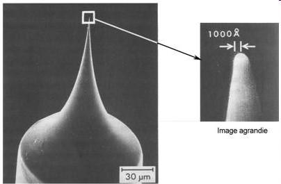
8 Electron Guns We want many electrons per time unit per area (high current density) and as small electron spot as possible Traditional guns: thermionic electron gun (electrons are emitted when a solid is heated) Modern: field emission guns (FEG) (cold guns, a strong electric field is used to extract electrons)

9 Electron Guns
 Image: Anders W. B.")
10 Detectors Backscattered electron detector: (Solid-State Detector) Secondary electron detector: (Everhart-Thornley) Image: Anders W. B. Skilbred, UiO
11 Our Traditional Detectors Secondary electrons: Everhart-Thornley Detector Backscattered electrons: Solid State Detector X-rays: Energy dispersive spectrometer (EDS)
12 Why do we need Vacuum? Chemical (corrosion!!) and thermal stability is necessary for a well-functioning filament (gun pressure) The signal electrons must travel from the sample to the detector (chamber pressure)
13 Sample Preparation All water must be removed from the sample All samples must also be trimmed to an apropriate size Metals no preparation Non-metalics cover the sample with a thin layer of a conductive material
 with a thin layer of gold.")

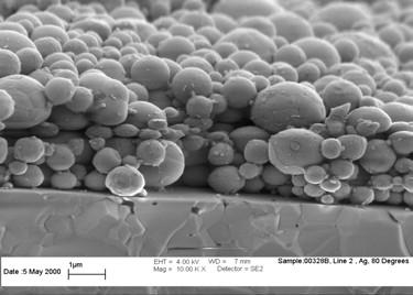
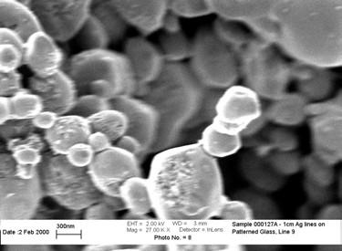
14 Sputter Coater The sputter coater is used to coat nonmetallic samples (bugs, plants, human hair, etc.) with a thin layer of gold. This makes them conductive, and ready to be viewed by the SEM. If the samples are metallic, they can simply be mounted and placed in the SEM.
15 High resolution of images A superior level of magnification A large dept of field Advantages Uses electromagnets as an alternative to lenses 3D data of sample can be measured Preparation of sample is relatively easy
16 Disadvantages Costly to purchase and maintain Sample have to be viewed in vacuum Non-conductive materials need coating Sensitive to vibration and external magnetic fields Sensitive to electrical supply SEMs are radiation-generating devices; so users need developing a 'SEM safety plan'
17 Summary The scanning electron microscope is a versatile instrument that can be used for many purposes and can be equipped with various accessories An electron probe is scanned across the surface of the sample and detectors interpret the signal as a function of time A resolution of 1 2 nm can be obtained when operated in a high resolution setup The introduction of ESEM and the field emission gun have simplified the imaging of challenging samples
18 Sem Application Fotos
19 Sem Application Fotos

20 Thanks For Your Attention
Gaetano L Episcopo. Scanning Electron Microscopy Focus Ion Beam and. Pulsed Plasma Deposition
 Gaetano L Episcopo Scanning Electron Microscopy Focus Ion Beam and Pulsed Plasma Deposition Hystorical background Scientific discoveries 1897: J. Thomson discovers the electron. 1924: L. de Broglie propose
SOLID STATE PHYSICS PHY F341. Dr. Manjuladevi.V Associate Professor Department of Physics BITS Pilani
 SOLID STATE PHYSICS PHY F341 Dr. Manjuladevi.V Associate Professor Department of Physics BITS Pilani 333031 manjula@bits-pilani.ac.in Characterization techniques SEM AFM STM BAM Outline What can we use
Scanning Electron Microscopy
 Scanning Electron Microscopy Amanpreet Kaur 1 www.reading.ac.uk/emlab Scanning Electron Microscopy What is scanning electron microscopy? Basic features of conventional SEM Limitations of conventional SEM
Scanning Electron Microscopy & Ancillary Techniques
 Scanning Electron Microscopy & Ancillary Techniques By Pablo G. Caceres-Valencia The prototype of the first Stereoscan supplied by the Cambridge Instrument Company to the dupont Company, U.S.A. (1965)
Modern Optical Spectroscopy
 Modern Optical Spectroscopy X-Ray Microanalysis Shu-Ping Lin, Ph.D. Institute of Biomedical Engineering E-mail: splin@dragon.nchu.edu.tw Website: http://web.nchu.edu.tw/pweb/users/splin/ Backscattered
Everhart-Thornley detector
 SEI Detector Everhart-Thornley detector Microscope chamber wall Faraday cage Scintillator Electrons in Light pipe Photomultiplier Electrical signal out Screen Quartz window +200 V +10 kv Always contains
Scanning Electron Microscopy
 Scanning Electron Microscopy Field emitting tip Grid 2kV 100kV Anode ZEISS SUPRA Variable Pressure FESEM Dr Heath Bagshaw CMA bagshawh@tcd.ie Why use an SEM? Fig 1. Examples of features resolvable using
Electron Microprobe Analysis and Scanning Electron Microscopy
 Electron Microprobe Analysis and Scanning Electron Microscopy Electron microprobe analysis (EMPA) Analytical technique in which a beam of electrons is focused on a sample surface, producing X-rays from
Chapter 10. Nanometrology. Oxford University Press All rights reserved.
 Chapter 10 Nanometrology Oxford University Press 2013. All rights reserved. 1 Introduction Nanometrology is the science of measurement at the nanoscale level. Figure illustrates where nanoscale stands
Why microscopy?
 Electron Microscopy Why microscopy? http://www.cellsalive.com/howbig.htm 2 Microscopes are used as magnifying tools (although not exclusively as will see later on). The resolution of the human eye is limited
Part II: Thin Film Characterization
 Part II: Thin Film Characterization General details of thin film characterization instruments 1. Introduction to Thin Film Characterization Techniques 2. Structural characterization: SEM, TEM, AFM, STM
= 6 (1/ nm) So what is probability of finding electron tunneled into a barrier 3 ev high?
 So what is probability of finding electron tunneled into a barrier 3 ev high?") STM STM With a scanning tunneling microscope, images of surfaces with atomic resolution can be readily obtained. An STM uses quantum tunneling of electrons to map the density of electrons on the surface
STM STM With a scanning tunneling microscope, images of surfaces with atomic resolution can be readily obtained. An STM uses quantum tunneling of electrons to map the density of electrons on the surface
Technical description of photoelectron spectrometer Escalab 250Xi
 Technical description of photoelectron spectrometer Escalab 250Xi Resource center Physical Methods of Surface Investigations 2014 Table of contents Common description 3 Analytical chamber 8 Preparation
Chapter 9. Electron mean free path Microscopy principles of SEM, TEM, LEEM
 Chapter 9 Electron mean free path Microscopy principles of SEM, TEM, LEEM 9.1 Electron Mean Free Path 9. Scanning Electron Microscopy (SEM) -SEM design; Secondary electron imaging; Backscattered electron
Electron Microprobe Analysis 1 Nilanjan Chatterjee, Ph.D. Principal Research Scientist
 12.141 Electron Microprobe Analysis 1 Nilanjan Chatterjee, Ph.D. Principal Research Scientist Massachusetts Institute of Technology Electron Microprobe Facility Department of Earth, Atmospheric and Planetary
Electron Microprobe Analysis 1 Nilanjan Chatterjee, Ph.D. Principal Research Scientist
 12.141 Electron Microprobe Analysis 1 Nilanjan Chatterjee, Ph.D. Principal Research Scientist Massachusetts Institute of Technology Electron Microprobe Facility Department of Earth, Atmospheric and Planetary
Introduction to Electron Beam Lithography
 Introduction to Electron Beam Lithography Boštjan Berčič (bostjan.bercic@ijs.si), Jožef Štefan Institute, Jamova 39, 1000 Ljubljana, Slovenia 1. Introduction Electron Beam Lithography is a specialized
ABC s of Electrochemistry series Materials Characterization techniques: SEM and EDS Ana María Valenzuela-Muñiz November 3, 2011
 ABC s of Electrochemistry series Materials Characterization techniques: SEM and EDS Ana María Valenzuela-Muñiz November 3, 2011 CEER, Department of Chemical and Biomolecular Engineering Outline Introduction
HOW TO APPROACH SCANNING ELECTRON MICROSCOPY AND ENERGY DISPERSIVE SPECTROSCOPY ANALYSIS. SCSAM Short Course Amir Avishai
 HOW TO APPROACH SCANNING ELECTRON MICROSCOPY AND ENERGY DISPERSIVE SPECTROSCOPY ANALYSIS SCSAM Short Course Amir Avishai RESEARCH QUESTIONS Sea Shell Cast Iron EDS+SE Fe Cr C Objective Ability to ask the
AP5301/ Name the major parts of an optical microscope and state their functions.
 Review Problems on Optical Microscopy AP5301/8301-2015 1. Name the major parts of an optical microscope and state their functions. 2. Compare the focal lengths of two glass converging lenses, one with
Dual Beam Helios Nanolab 600 and 650
 Dual Beam Helios Nanolab 600 and 650 In the Clean Room facilities of the INA LMA, several lithography facilities permit to pattern structures at the micro and nano meter scale and to create devices. In
Nova 600 NanoLab Dual beam Focused Ion Beam IITKanpur
 Nova 600 NanoLab Dual beam Focused Ion Beam system @ IITKanpur Dual Beam Nova 600 Nano Lab From FEI company (Dual Beam = SEM + FIB) SEM: The Electron Beam for SEM Field Emission Electron Gun Energy : 500
Model : JEOL JSM 7610f
 Name Field Emission Electron Scanning Microscopy (FESEM) Make: JEOL India Pvt Ltd. Model : JEOL JSM 7610f Specification Electron gun : Schottky type field emission (T-FE) gun Electron Beam resolution (secondary
Basic Principles Brief history of EM
 SIR WILLIAM DUNN SCHOOL OF PATHOLOGY Basic Principles of Electron Microscopy (EM) Dr Errin Johnson Head of the Dunn School EM Facility Basic Principles Brief history of EM 1873 Hermann von Helmholtz &
THIN FILMS FOR PHOTOVOLTAICS AND OTHER APPLICATIONS. BY Dr.A.K.SAXENA PHOTONICS DIVISION INDIAN INSTITUTE OF ASTROPHYSICS
 THIN FILMS FOR PHOTOVOLTAICS AND OTHER APPLICATIONS BY Dr.A.K.SAXENA PHOTONICS DIVISION INDIAN INSTITUTE OF ASTROPHYSICS BACKGROUND 2.8 meter coating plant at VBO, Kavalur 1.5 meter coating plant at VBO,
MEMS Metrology. Prof. Tianhong Cui ME 8254
 MEMS Metrology Prof. Tianhong Cui ME 8254 What is metrology? Metrology It is the science of weights and measures Refers primarily to the measurements of length, weight, time, etc. Mensuration- A branch
An Introduction to Auger Electron Spectroscopy
 An Introduction to Auger Electron Spectroscopy Spyros Diplas MENA3100 SINTEF Materials & Chemistry, Department of Materials Physics & Centre of Materials Science and Nanotechnology, Department of Chemistry,
Analytical Methods for Materials
 Analytical Methods for Materials Lesson 21 Electron Microscopy and X-ray Spectroscopy Suggested Reading Leng, Chapter 3, pp. 83-126; Chapter 4, pp. 127-160; Chapter 6, pp. 191-219 P.J. Goodhew, J. Humphreys
Electron beam scanning
 Electron beam scanning The Electron beam scanning operates through an electro-optical system which has the task of deflecting the beam Synchronously with cathode ray tube which create the image, beam moves
A DIVISION OF ULVAC-PHI. Quantera II. Scanning XPS Microprobe
 A DIVISION OF ULVAC-PHI Quantera II Scanning XPS Microprobe X-ray Photoelectron Spectroscopy (XPS/ESCA) is the most widely used surface analysis technique and has many well established industrial and
Remote Access to Hi-tech Equipment
 Remote Access to Hi-tech Equipment From Your Classroom to Ours Sebastien Maeder Outline What is Remote Access? The Method vs. the Goal The role within NACK Why should we try? Confines of Classroom Characterization
Ecole Franco-Roumaine : Magnétisme des systèmes nanoscopiques et structures hybrides - Brasov, Modern Analytical Microscopic Tools
 1. Introduction Solid Surfaces Analysis Group, Institute of Physics, Chemnitz University of Technology, Germany 2. Limitations of Conventional Optical Microscopy 3. Electron Microscopies Transmission Electron
SEM Doctoral Course MS-636. April 11-13, 2016
 Thomas LaGrange, Ph.D. Faculty Lecturer and Senior Staff Scientist Electron Sources, Optics and Detectors SEM Doctoral Course MS-636 April 11-13, 2016 Summary Electron propagation is only possible through
PHI 5000 Versaprobe-II Focus X-ray Photo-electron Spectroscopy
 PHI 5000 Versaprobe-II Focus X-ray Photo-electron Spectroscopy The very basic theory of XPS XPS theroy Surface Analysis Ultra High Vacuum (UHV) XPS Theory XPS = X-ray Photo-electron Spectroscopy X-ray
CHARACTERIZATION of NANOMATERIALS KHP
 CHARACTERIZATION of NANOMATERIALS Overview of the most common nanocharacterization techniques MAIN CHARACTERIZATION TECHNIQUES: 1.Transmission Electron Microscope (TEM) 2. Scanning Electron Microscope
MSE 321 Structural Characterization
 Optical Microscope Plan Lenses In an "ideal" single-element lens system all planar wave fronts are focused to a point at distance f from the lens; therefore: Image near the optical axis will be in perfect
The Effect of Magnetic Field Direction on the Imaging Quality of Scanning Electron Microscope
 Journal of Magnetics (), 49-54 (07) ISSN (Print) 6-750 ISSN (Online) 33-6656 https://doi.org/0.483/jmag.07...049 The Effect of Magnetic Field Direction on the Imaging Quality of Scanning Electron Microscope
Practical course in scanning electron microscopy
 Practical course in scanning electron microscopy Fortgeschrittenen Praktikum an der Technischen Universität München Wintersemester 2017/2018 Table of contents 1. Introduction 3 2. Formation of an electron
tip conducting surface
 PhysicsAndMathsTutor.com 1 1. The diagram shows the tip of a scanning tunnelling microscope (STM) above a conducting surface. The tip is at a potential of 1.0 V relative to the surface. If the tip is sufficiently
Chapter 12. Nanometrology. Oxford University Press All rights reserved.
 Chapter 12 Nanometrology Introduction Nanometrology is the science of measurement at the nanoscale level. Figure illustrates where nanoscale stands in relation to a meter and sub divisions of meter. Nanometrology
Imaging Methods: Scanning Force Microscopy (SFM / AFM)
") Imaging Methods: Scanning Force Microscopy (SFM / AFM) The atomic force microscope (AFM) probes the surface of a sample with a sharp tip, a couple of microns long and often less than 100 Å in diameter.
Imaging Methods: Scanning Force Microscopy (SFM / AFM) The atomic force microscope (AFM) probes the surface of a sample with a sharp tip, a couple of microns long and often less than 100 Å in diameter.
A DIVISION OF ULVAC-PHI
 A DIVISION OF ULVAC-PHI X-ray photoelectron spectroscopy (XPS/ESCA) is the most widely used surface analysis technique and has many well established industrial and research applications. XPS provides
How to distinguish EUV photons from out-of-band photons
 How to distinguish EUV photons from out-of-band photons Thesis submitted in partial fulfillment of the requirements for the degree of Master of Science in Physics Author: Student ID: Supervisors: 2 nd
MT Electron microscopy Scanning electron microscopy and electron probe microanalysis
 MT-0.6026 Electron microscopy Scanning electron microscopy and electron probe microanalysis Eero Haimi Research Manager Outline 1. Introduction Basics of scanning electron microscopy (SEM) and electron
Characterization of Secondary Emission Materials for Micro-Channel Plates. S. Jokela, I. Veryovkin, A. Zinovev
 Characterization of Secondary Emission Materials for Micro-Channel Plates S. Jokela, I. Veryovkin, A. Zinovev Secondary Electron Yield Testing Technique We have incorporated XPS, UPS, Ar-ion sputtering,
Secondary Ion Mass Spectrometry (SIMS)
") CHEM53200: Lecture 10 Secondary Ion Mass Spectrometry (SIMS) Major reference: Surface Analysis Edited by J. C. Vickerman (1997). 1 Primary particles may be: Secondary particles can be e s, neutral species
CHEM53200: Lecture 10 Secondary Ion Mass Spectrometry (SIMS) Major reference: Surface Analysis Edited by J. C. Vickerman (1997). 1 Primary particles may be: Secondary particles can be e s, neutral species
á1181ñ SCANNING ELECTRON MICROSCOPY
 USP 40 General Information / á1181ñ Scanning Electron Microscopy 1 á1181ñ SCANNING ELECTRON MICROSCOPY INTRODUCTION Over the last few decades, electron microscopy has become a reliable investigative tool
INDIAN INSTITUTE OF TECHNOLOGY ROORKEE NPTEL NPTEL ONLINE CERTIFICATION COURSE. Biomedical Nanotechnology. Lec-05 Characterisation of Nanoparticles
 INDIAN INSTITUTE OF TECHNOLOGY ROORKEE NPTEL NPTEL ONLINE CERTIFICATION COURSE Biomedical Nanotechnology Lec-05 Characterisation of Nanoparticles Dr. P. Gopinath Department of Biotechnology Indian Institute
Massachusetts Institute of Technology. Dr. Nilanjan Chatterjee
 Massachusetts Institute of Technology Dr. Nilanjan Chatterjee Electron Probe Micro-Analysis (EPMA) Imaging and micrometer-scale chemical compositional analysis of solids Signals produced in The Electron
Kavli Workshop for Journalists. June 13th, CNF Cleanroom Activities
 Kavli Workshop for Journalists June 13th, 2007 CNF Cleanroom Activities Seeing nm-sized Objects with an SEM Lab experience: Scanning Electron Microscopy Equipment: Zeiss Supra 55VP Scanning electron microscopes
object objective lens eyepiece lens
 Advancing Physics G495 June 2015 SET #1 ANSWERS Field and Particle Pictures Seeing with electrons The compound optical microscope Q1. Before attempting this question it may be helpful to review ray diagram
STUDY AND ANALYSIS OF THE FAILED USB DEVICES USED IN COPPER MINE USING ENVIRONMENTAL SCANNING ELECTRON MICROSCOPY AND X-RAY PHOTOELECTRON SPECTROSCOPY
 STUDY AND ANALYSIS OF THE FAILED USB DEVICES USED IN COPPER MINE USING ENVIRONMENTAL SCANNING ELECTRON MICROSCOPY AND X-RAY PHOTOELECTRON SPECTROSCOPY Ayush Garg Department of Chemical and Materials Engineering,
Invited Lecture. "Different Aspects of Electron Microscopy. Sardar Vallabhbhai National Institute of Technology, Surat. Deepak Rajput & S.K.
 Invited Lecture on "Different Aspects of Electron Microscopy at Sardar Vallabhbhai National Institute of Technology, Surat Deepak Rajput & S.K. Tiwary R&D and Product Development Essar Steel Limited Abstract
Characterisation of Catalysts Using Secondary and Backscattered Electron In-lens Detectors
 Platinum Metals Rev., 2014, 58, (2), 106 110 FINAL ANALYSIS Characterisation of Catalysts Using Secondary and Backscattered Electron In-lens Detectors Heterogeneous catalysis often involves the use of
MSE 321 Structural Characterization
 Auger Spectroscopy Auger Electron Spectroscopy (AES) Scanning Auger Microscopy (SAM) Incident Electron Ejected Electron Auger Electron Initial State Intermediate State Final State Physical Electronics
Information from Every Angle
 pplication Note Information from Every ngle Directional SE Detector for Next-Level Imaging Zinc oxide nanorods with surficial palladium particles imaged at 500 V in high vacuum. dding palladium increases
Methods of surface analysis
 Methods of surface analysis Nanomaterials characterisation I RNDr. Věra Vodičková, PhD. Surface of solid matter: last monoatomic layer + absorbed monolayer physical properties are effected (crystal lattice
Basic structure of SEM
 Table of contents Basis structure of SEM SEM imaging modes Comparison of ordinary SEM and FESEM Electron behavior Electron matter interaction o Elastic interaction o Inelastic interaction o Interaction
E-Guide. Sample Preparation. A guide to ideal sample preparation
 E-Guide Sample Preparation A guide to ideal sample preparation Contents Introduction 3 1. Basic sample preparation 4 2. Non-conductive samples 5 2.1 Use of conductive coating 2.2 Low vacuum 2.3 Sputter
3 Scanning Electron Microscopy
 3 Scanning Electron Microscopy David C. Joy University of Tennessee, Knoxville, TN, U.S.A. List of Symbols and Abbreviations 222 3.1 Introduction and Historical Summary 223 3.2 Principles of the Scanning
EM-30AX is very good space utilization
 EM helps to grasp material characteristics through providing precise images. EM makes it possible to analyze deep submicron or nanometer structure. Alteration of material caused by pressure, heat can be
The illumination source: the electron beam
 The SEM Column The illumination source: the electron beam The probe of the electron microscope is an electron beam with very high and stable energy (10-100 kev) in order to get images with high resolution.
Secondary Ion Mass Spectroscopy (SIMS)
") Secondary Ion Mass Spectroscopy (SIMS) Analyzing Inorganic Solids * = under special conditions ** = semiconductors only + = limited number of elements or groups Analyzing Organic Solids * = under special
Secondary Ion Mass Spectroscopy (SIMS) Analyzing Inorganic Solids * = under special conditions ** = semiconductors only + = limited number of elements or groups Analyzing Organic Solids * = under special
Secondary ion mass spectrometry (SIMS)
") Secondary ion mass spectrometry (SIMS) ELEC-L3211 Postgraduate Course in Micro and Nanosciences Department of Micro and Nanosciences Personal motivation and experience on SIMS Offers the possibility to
Secondary ion mass spectrometry (SIMS) ELEC-L3211 Postgraduate Course in Micro and Nanosciences Department of Micro and Nanosciences Personal motivation and experience on SIMS Offers the possibility to
CBE Science of Engineering Materials. Scanning Electron Microscopy (SEM)
") CBE 30361 Science of Engineering Materials Scanning Electron Microscopy (SEM) Scale of Structure Organization Units: micrometer = 10-6 m = 1µm nanometer= 10-9 m = 1nm Angstrom = 10-10 m = 1Å A hair is
CBE 30361 Science of Engineering Materials Scanning Electron Microscopy (SEM) Scale of Structure Organization Units: micrometer = 10-6 m = 1µm nanometer= 10-9 m = 1nm Angstrom = 10-10 m = 1Å A hair is
An Experimental Study to Show the Effects of Secondary Electron Emission on Plasma Properties in Hall Thrusters
 An Experimental Study to Show the Effects of Secondary Electron Emission on Plasma Properties in Hall Thrusters Kapil U. Sawlani and John E. Foster Plasma Science and Technology Laboratory Nuclear Engineering
Notice Basic Information Estimated Contract Value (USD) $35, (Not shown to suppliers) Reference Number Issuing Organization
 $35, (Not shown to suppliers) Reference Number Issuing Organization") Notice Basic Information Estimated Contract Value (USD) $35,000.00 (Not shown to suppliers) Reference Number 0000195967 Issuing Organization Colorado Mesa University Owner Organization Colorado Mesa University
Notice Basic Information Estimated Contract Value (USD) $35,000.00 (Not shown to suppliers) Reference Number 0000195967 Issuing Organization Colorado Mesa University Owner Organization Colorado Mesa University
MT Electron microscopy Scanning electron microscopy and electron probe microanalysis
 MT-0.6026 Electron microscopy Scanning electron microscopy and electron probe microanalysis Eero Haimi Research Manager Outline 1. Introduction Basics of scanning electron microscopy (SEM) and electron
Nano-Microscopy. Lecture 2. Scanning and Transmission Electron Microscopies: Principles. Pavel Zinin HIGP, University of Hawaii, Honolulu, USA
 GG 711: Advanced Techniques in Geophysics and Materials Science Nano-Microscopy. Lecture 2 Scanning and Transmission Electron Microscopies: Principles Pavel Zinin HIGP, University of Hawaii, Honolulu,
Low Vacuum Scanning Electron Microscopy and Microanalysis
 Low Vacuum Scanning Electron Microscopy and Microanalysis Principles and Practice of Variable Pressure/Environmental Scanning Electron Microscopy (VP-ESEM), Debbie J Stokes, John Wiley&Sons 2008 Several
PHYSICS ORDINARY LEVEL
 *B16* PRE-LEAVING CERTIFICATE EXAMINATION, 2011 PHYSICS ORDINARY LEVEL TIME: 3 HOURS Answer three questions from section A and five questions from section B. Page 1 of 10 SECTION A (120 marks) Answer three
Controlled double-slit electron diffraction
 1 Controlled double-slit electron diffraction Roger Bach 1, Damian Pope 2, Sy-Hwang Liou 1 and Herman Batelaan 1 1 Department of Physics and Astronomy, University of Nebraska-Lincoln, Theodore P. Jorgensen
h p λ = mν Back to de Broglie and the electron as a wave you will learn more about this Equation in CHEM* 2060
 Back to de Broglie and the electron as a wave λ = mν h = h p you will learn more about this Equation in CHEM* 2060 We will soon see that the energies (speed for now if you like) of the electrons in the
NOTE FIBROUS CLAY MINERAL COLLAPSE PRODUCED BY BEAM DAMAGE OF CARBON-COATED SAMPLES DURING SCANNING ELECTRON MICROSCOPY
 Clay Minerals (1991) 26, 141-145 NOTE FIBROUS CLAY MINERAL COLLAPSE PRODUCED BY BEAM DAMAGE OF CARBON-COATED SAMPLES DURING SCANNING ELECTRON MICROSCOPY Authigenic fibrous clays often occur in the pore
History of 3D Electron Microscopy and Helical Reconstruction
 T H E U N I V E R S I T Y of T E X A S S C H O O L O F H E A L T H I N F O R M A T I O N S C I E N C E S A T H O U S T O N History of 3D Electron Microscopy and Helical Reconstruction For students of HI
Particle Analysis of Environmental Swipe Samples
 IAEA-SM-367/10/07 Particle Analysis of Environmental Swipe Samples D. DONOHUE, S. VOGT, A. CIURAPINSKI, F. RUEDENAUER, M. HEDBERG Safeguards Analytical Laboratory International Atomic Energy Agency Vienna,
Questions/Answers. Chapter 1
 Questions/Answers Chapter 1 1.1 What are the advantages of the SEM over optical microscopy? Advantages: Higher resolution and greater depth of field and microchemical analysis Disadvantages: Expensive,
Gestão e Produção Sustentável. Durability Electromagnetic radiation. ENG K49 Materiais de origem vegetal aplicados na construção
 Gestão e Produção Sustentável Durability Electromagnetic radiation ENG K49 Materiais de origem vegetal aplicados na construção Ricardo Fernandes Carvalho Electromagnetic radiation spectral band Microwaves
Auger Electron Spectroscopy Overview
 Auger Electron Spectroscopy Overview Also known as: AES, Auger, SAM 1 Auger Electron Spectroscopy E KLL = E K - E L - E L AES Spectra of Cu EdN(E)/dE Auger Electron E N(E) x 5 E KLL Cu MNN Cu LMM E f E
MSE 321 Structural Characterization
 Auger Spectroscopy Auger Electron Spectroscopy (AES) Scanning Auger Microscopy (SAM) Incident Electron Ejected Electron Auger Electron Initial State Intermediate State Final State Physical Electronics
SCANNING-PROBE TECHNIQUES OR APPARATUS; APPLICATIONS OF SCANNING-PROBE TECHNIQUES, e.g. SCANNING PROBE MICROSCOPY [SPM]
![SCANNING-PROBE TECHNIQUES OR APPARATUS; APPLICATIONS OF SCANNING-PROBE TECHNIQUES, e.g. SCANNING PROBE MICROSCOPY [SPM]](/thumbs/81/83165631.jpg "SCANNING-PROBE TECHNIQUES OR APPARATUS; APPLICATIONS OF SCANNING-PROBE TECHNIQUES, e.g. SCANNING PROBE MICROSCOPY [SPM]") G01Q SCANNING-PROBE TECHNIQUES OR APPARATUS; APPLICATIONS OF SCANNING-PROBE TECHNIQUES, e.g. SCANNING PROBE MICROSCOPY [SPM] Scanning probes, i.e. devices having at least a tip of nanometre sized dimensions
G01Q SCANNING-PROBE TECHNIQUES OR APPARATUS; APPLICATIONS OF SCANNING-PROBE TECHNIQUES, e.g. SCANNING PROBE MICROSCOPY [SPM] Scanning probes, i.e. devices having at least a tip of nanometre sized dimensions
Unit title: Atomic and Nuclear Physics for Spectroscopic Applications
 Unit title: Atomic and Nuclear Physics for Spectroscopic Applications Unit code: Y/601/0417 QCF level: 4 Credit value: 15 Aim This unit provides an understanding of the underlying atomic and nuclear physics
Auger Electron Spectroscopy
 Auger Electron Spectroscopy Auger Electron Spectroscopy is an analytical technique that provides compositional information on the top few monolayers of material. Detect all elements above He Detection
Part I Basics and Methods
 j1 Part I Basics and Methods In-situ Electron Microscopy: Applications in Physics, Chemistry and Materials Science, First Edition. Edited by Gerhard Dehm, James M. Howe, and Josef Zweck. Ó 2012 Wiley-VCH
Transmission Electron Microscopy
 L. Reimer H. Kohl Transmission Electron Microscopy Physics of Image Formation Fifth Edition el Springer Contents 1 Introduction... 1 1.1 Transmission Electron Microscopy... 1 1.1.1 Conventional Transmission
User Fees for the 4D LABS Characterization Facility
 User Fees for the 4D LABS Characterization Facility 1. Imaging Fees Service SEM 1 - Helios: SEM/EDS mode SEM/EDS mode with FIB functions Cryo mode setup SEM 2 Nova NanoSEM SEM/EDS mode SEM/EDS mode with
Auger Electron Spectroscopy (AES)
") 1. Introduction Auger Electron Spectroscopy (AES) Silvia Natividad, Gabriel Gonzalez and Arena Holguin Auger Electron Spectroscopy (Auger spectroscopy or AES) was developed in the late 1960's, deriving
1. Introduction Auger Electron Spectroscopy (AES) Silvia Natividad, Gabriel Gonzalez and Arena Holguin Auger Electron Spectroscopy (Auger spectroscopy or AES) was developed in the late 1960's, deriving
(a) (i) State the proton number and the nucleon number of X.
 (i) State the proton number and the nucleon number of X.") PhysicsAndMathsTutor.com 1 1. Nuclei of 218 84Po decay by the emission of an particle to form a stable isotope of an element X. You may assume that no emission accompanies the decay. (a) (i) State the
PhysicsAndMathsTutor.com 1 1. Nuclei of 218 84Po decay by the emission of an particle to form a stable isotope of an element X. You may assume that no emission accompanies the decay. (a) (i) State the
Low kv Scanning Electron Microscopy
 4 Low kv Scanning Electron Microscopy M. David Frey 1. Introduction The voltages typically associated with low-voltage scanning electron microscopy are within the range of 5 kv and lower. The low end cutoff
TESCAN S New generation of FIB-SEM microscope
 TESCAN S New generation of FIB-SEM microscope rising standards in sample preparation Key Features SEM COLUMN Versatile system for unlimited applications: resolution imaging (0.9 nm at 15 kev, 1.4 nm at
MODERN TECHNIQUES OF SURFACE SCIENCE
 MODERN TECHNIQUES OF SURFACE SCIENCE Second edition D. P. WOODRUFF & T. A. DELCHAR Department ofphysics, University of Warwick CAMBRIDGE UNIVERSITY PRESS Contents Preface to first edition Preface to second
UNIVERSITI SAINS MALAYSIA
 UNIVERSITI SAINS MALAYSIA First Semester Examination Academic Session 2009/2010 November 2009 EBB 511/3 - Materials Characterisation Techniques Duration : 3 hours Please ensure that this examination paper
SEM Optics and Application to Current Research
 SEM Optics and Application to Current Research Azure Avery May 28, 2008 1 Introduction 1.1 History The optical microscope was invented in the early 17th century. Although revolutionary, the earliest microscopes
Supporting Online Material for
 www.sciencemag.org/cgi/content/full/1142021/dc1 Supporting Online Material for Remnants of the Early Solar System Water Enriched in Heavy Oxygen Isotopes Naoya Sakamoto, Yusuke Seto, Shoichi Itoh, Kiyoshi
Surface Analytical Techniques for Analysis of Coatings Mary Jane Walzak, Mark Biesinger and Brad Kobe The University of Western Ontario, Surface
 Surface Analytical Techniques for Analysis of Coatings Mary Jane Walzak, Mark Biesinger and Brad Kobe The University of Western Ontario, Surface Science Western 999 Collip Circle, Room LL31, London, ON
Nanotechnology and Characterization of Nanomaterials
 Abstract Nanotechnology and Characterization of Nanomaterials Mrs Usha Raghavan Head, Information Technology VPM s Polytechnic, Thane Email: usharagha@gmail.com There s plenty of room at the bottom said
Microscopy, Staining, and Classification
 PowerPoint Lecture Presentations prepared by Mindy Miller-Kittrell, North Carolina State University C H A P T E R 4 Microscopy, Staining, and Classification Microscopy Light Microscopy 1) Bright-field
accelerating opportunities
 accelerating opportunities 9 MV Pelletron FN Tandem Accelerator for basic and applied research The 9MV Tandem Accelerator has been built by the High Voltage Engineering Corporation (HVEC) in 1973 and it
Ma5: Auger- and Electron Energy Loss Spectroscopy
 Ma5: Auger- and Electron Energy Loss Spectroscopy 1 Introduction Electron spectroscopies, namely Auger electron- and electron energy loss spectroscopy are utilized to determine the KLL spectrum and the
ENERGY DISPERSIVE X-RAY ANALYSIS OF HUMAN HAIR Mohd Abdul Mujeeb 1 and Kahlid M Zafar 2
 International Journal of Science, Environment and Technology, Vol. 6, No 3, 2017, 2036 2040 ISSN 2278-3687 (O) 2277-663X (P) ENERGY DISPERSIVE X-RAY ANALYSIS OF HUMAN HAIR Mohd Abdul Mujeeb 1 and Kahlid