NATO Advanced Research Workshop on Fundamental and Applied NanoElectroMagnetics (FANEM), May 25-27, 2015, Minsk, Belarus.
|
|
|
- Imogene Wilcox
- 5 years ago
- Views:
Transcription


1 NATO Advanced Research Workshop on Fundamental and Applied NanoElectroMagnetics (FANEM), May 25-27, 2015, Minsk, Belarus 2D Crystals for Nanoelectronics and Beyond.. Kaustav Banerjee Department of Electrical and Computer Engineering University of California, anta Barbara, CA May 25, 2015


2 . Borkar (Intel) 1.6X 6X Dragon Energy On-die global interconnect energy scales slower than compute On-die data movement energy will start to dominate K. Banerjee et al., IEEE Trans. Electron Devices, 49(11), pp , Need Green Transistors Need Green Interconnects

 (E g >5eV)")
")
 ilicine")
 VO")

")


3 2D Electronic Materials Family Tree Graphene family TMD family h-bn (dielectric) (E g >5eV) Nbe 2, etc (superconductor) Graphene (semi-metal) (E g =0eV) ilicine (semiconductor) (E g =0.6 ev, experimentally) VO 2, V 2, etc (metals) Mo 2, We 2, etc (semiconductors) CrO 2, Cr 2, etc (half-metals) (0<E g <1eV) Other families Ti 2 C, Ti 2 CF 2 Black Phosphorus etc. Kaustav Banerjee, UC anta Barbara kaustav@ece.ucsb.edu May 25, 2015, FANEM Workshop 3


")


4 few Å 1.2 nm deep Oxide Advantages of 2D Materials (1/2) Potato-like 3D Materials Increased EOT Gate Degraded Channel Potential (V Ch ) Gate C G C C Channel C DC D Covalent bonds everywhere Mobile charges centroid V Ch CG C C C G C DC V G Onion-like 2D Materials Gate Advanced Topology & Controllable V Ch Layered structure Covalent bonds Can be exfoliated Van der Waals force few Å Carriers confined Gate Oxide Channel ubstrate Gate Oxide Oxide Gate D D Thin Channel: Low C C, C DC Kaustav Banerjee, UC anta Barbara kaustav@ece.ucsb.edu May 25, 2015, FANEM Workshop 4

 EC Eg EV Covalent bonds")


5 Advantages of 2D Materials (2/2) Potato-like 3D Materials Thickness Roughness Band gap Variation Performance Variation Interface Variations (Traps) Unsaturated atoms on surfaces Dangling bonds (traps) EC Eg EV Covalent bonds everywhere Onion-like 2D Materials Layered structure Covalent bonds Controllable # of Layers Controllable Band gaps Pristine Interfaces (No interface traps) aturated atoms Can be exfoliated Dirac Point Ec 5 Ev No dangling bonds Van der Waals force Graphene h-bn Mo2 We2 few Å Kaustav Banerjee, UC anta Barbara kaustav@ece.ucsb.edu May 25, 2015, FANEM Workshop 5


6 2D Materials UCB Devices, Interconnects, Circuits Key Issues in 2D Device Design Contact Doping dopant Interface Contact Doping Interface Mo 2 Explore Green Devices/Circuits and Applications: CMO and Beyond 2D Material election and FET Design for ITR Roadmap Novel Heterostructures and Devices (2D Tunnel-FETs) Flexible and Transparent 2D Circuits/ensors Kaustav Banerjee, UC anta Barbara kaustav@ece.ucsb.edu May 25, 2015, FANEM Workshop 6


7 Understanding and Optimizing Metal-TMD Contacts J. Kang, W. Liu, D. arkar, D. Jena and K. Banerjee, Phys. Rev. X, Vol. 4, No. 3, pp , Tunnel barrier chottky barrier Orbital overlap Treatment of vdw force in DFT (bulk metal-tmd) for the first time Widest diversity of metals and TMDs First study of metal-tmd edge contacts Fermi level pinning revealed beyond chottky theory Kaustav Banerjee, UC anta Barbara May 25, 2015, FANEM Workshop 7
 Contact Engineered TMD FETs Guided by DFT First")

 3L Optical Image 2L 1L High mobility: 142 cm 2 /V.")

")

8 R (kω.μm) Contact Engineered TMD FETs Guided by DFT First High-Performance Monolayer n-type We 2 FET W. Liu, J. Kang, D. arkar, Y. Khatami, D. Jena and K. Banerjee, Nano Lett., Vol. 13, no. 5, pp , (a) 3L Optical Image 2L 1L High mobility: 142 cm 2 /V.s Record I ON : 210 µa/µm High-Performance Mo 2 FET with Mo Contacts J. Kang, W. Liu and K. Banerjee, App. Phys. Lett.,104, 9, , Mo Mo Mo Mo Mo Mo Mo Mo Mo Mo Mo Mo Mo trong bonding (Å -3 ) Mo Optical Image EM Image R total = R channel +2 R total R channel R contact 4 layers R contact 2 kω.μm V bg (V) Kaustav Banerjee, UC anta Barbara kaustav@ece.ucsb.edu May 25, 2015, FANEM Workshop 8

 Both n- and p-type are")

9 Doping of TMDs using Metallic Nanoparticles D. arkar, X. Xie, J. Kang, H. Zhang, W. Liu, J. Navarrete, M. Moskovits and K. Banerjee, Nano Letters, vol. 15, no. 5, pp , Back-gate Vth shift up to 137 V (monolayer Mo 2 FET) Both n- and p-type are available First p-type doping of We 2 FET imple/effective/table way of doping as well as sensing Metal Mo 2 4 nm Doping Hydrogen Gas ensing 50 nm Kaustav Banerjee, UC anta Barbara kaustav@ece.ucsb.edu May 25, 2015, FANEM Workshop 9


10 Understanding TMD-Dielectric Interfaces J. Kang, W. Liu and K. Banerjee, 45 th IEEE IC, Dec , an Diego, pp. 1-2, Mo 2 H O io dipoles + - H O Mo 2 trap Interfaces hold the key to device performance Revealing microscopic physics of 2D-dielectric interfaces Dipoles/traps evaluated atomically Compared 5 dielectrics h-bn buffer layer is preferred io 2 Mo 2 h-bn HfO 2 Kaustav Banerjee, UC anta Barbara kaustav@ece.ucsb.edu May 25, 2015, FANEM Workshop 10


11 Interface Characterization: Low-Frequency Noise X. Xie, D. arkar, W. Liu, J. Kang, O. Marinov, M. J. Deen and K. Banerjee, AC Nano, Vol. 8, No. 6, pp , PR residue Low-frequency noise in bilayer Mo 2 field-effect transistor Mo 2 Existence and hift of Noise Peak io 2 before annealing after annealing 10-5 Noise Peak before annealing Interface vdw gaps induce noise peak in 2D materials The first theoretical model explaining the noise peaks in 2D materials Annealing process reduces noise Noise Peak after annealing V G (V) Kaustav Banerjee, UC anta Barbara kaustav@ece.ucsb.edu May 25, 2015, FANEM Workshop 11

 Ids ( x) qwn2 D( x) ( x) dx IV.")
12 Compact Modeling for Circuit Exploration & tudying Effects of Parameter Variation First Physics based Compact Model for 2D TMD FET W. Cao, J. Kang, W. Liu and K. Banerjee, IEEE Trans. Electron Devices, 61, 12, , Model available on: I. tart from fundamental: Gauss s law II. Develop a modified Poisson s equation specifically for 2D channel 2 d 2 2 dx q( n N ) 2D T 2D 2D imp n2 DO2 ( E) f ( E E ) de D D F E c DO g g m * s i i 2D 2 i 1,2 2 III. Use Drift-Diffusion equation for current transport dv ( x) Ids ( x) qwn2 D( x) ( x) dx IV. Explicit intrinsic drain current expression obtained I ds T qw q 0 L T q 2D 2D 2D 2D 2 kt ( ) 2 Nimp D q 2 2 D 2 Kaustav Banerjee, UC anta Barbara kaustav@ece.ucsb.edu May 25, 2015, FANEM Workshop 12

, Berkeley 2012 We 2 (for electron), UCB 2013 Direct Tunneling Ch D Mobility (cm 2 /V s)")
 NU 2014 HP Black P (high-m direction) Renmin Univ. 2014 60 W 2 Mo 2 Yonsei Univ.")
13 Tunnel Leakage Carrier Velocity 2D FET Material election for ITR 2026 (5.9 nm) W. Cao, J. Kang, D. arkar, W. Liu and K. Banerjee, IEDM 2014, pp Germanane OU 2013 We 2 (for hole), Berkeley 2012 We 2 (for electron), UCB 2013 Direct Tunneling Ch D Mobility (cm 2 /V s) LTP Black P (low-m direction) Renmin Univ ilicane ( low-m direction) NU 2014 HP Black P (high-m direction) Renmin Univ W 2 Mo 2 Yonsei Univ Moe 2 EPFL 2011 UT Austin 2012 UCB Effective Mass m (m 0 ) Effective mass should be in suitable region T e a m v k m HP: High Performance m LTP: Low tandby Power Improving mobility only does not work for 5.9 nm node! m Kaustav Banerjee, UC anta Barbara kaustav@ece.ucsb.edu May 25, 2015, FANEM Workshop 13
 olid-state devices = Δlog(Id ) V th ΔV gs V G I OFF E C E V ource Drain Channel 60 mv/dec. ource < 60 mv/dec.")

14 log(i D ) An ideal switch Boltzmann tail 2D Band-to-Band Tunneling FET Y. Khatami and K. Banerjee, IEEE Trans. Electron Devices, 56(11), pp , MOFET Boltzmann tail TFET ΔV gs Δlog(I d ) olid-state devices = Δlog(Id ) V th ΔV gs V G I OFF E C E V ource Drain Channel 60 mv/dec. ource < 60 mv/dec. I OFF E C E V Channel Drain Advantages of 2D TFET: Heterojunctions with low band overlap Better electrostatics mall tunneling barrier width Pristine interfaces W. Cao, D. arkar, Y. Khatami, J. Kang and K. Banerjee, AIP Advances, 4, , Kaustav Banerjee, UC anta Barbara kaustav@ece.ucsb.edu May 25, 2015, FANEM Workshop 14

15 Minimum Delay (s) Dynamic Power (W) Noise Margin (/VDD) Inverter Gain All-Graphene Logic Circuits Making Interconnects and Transistors with the same Material J. Kang, D. arkar, Y. Khatami and K. Banerjee, Appl. Phys. Lett., Vol. 103, No. 8, , Performance Evaluation Inverter Noise Margin Inverter Gain V DD (V) V DD (V) Inverter Delay Power Consumption HP-CMO Few Fabrication teps Low Contact Resistance Higher Performances over CMO V DD (V) Max Frequency (Hz) All-Graphene Monolithic Logic Circuits 22nm-CMO 22nm-CMO (High (Low Power Model) Performance Model) Kaustav Banerjee, UC anta Barbara kaustav@ece.ucsb.edu May 25, 2015, FANEM Workshop 15


16 First Demonstration of 2D TMD FET Biosensor D. arkar, W. Liu, X. Xie, A. Anselmo,. Mitragotri and K. Banerjee., AC Nano, 8 (4), pp , Label Free - Fast -Low-Cost Kaustav Banerjee, UC anta Barbara kaustav@ece.ucsb.edu May 25, 2015, FANEM Workshop 17

 10 5 X receptor molecules D graphene channel")
 TFET Biosensor in Research")

17 Ultra-Low Power and Ultra-ensitive Tunnel-FET Biosensors D. arkar and K. Banerjee, Appl. Phys. Lett., 100, , target biomolecules G Boltzmann tail (e - density) E C E C (BTB Tunnel Current) 10 5 X receptor molecules D graphene channel After conjugation E V ource Barrier Channel ON Current OFF Current Drain (Nearly No Leakage) TFET Biosensor in Research Highlights of Nature Nanotechnology D. arkar and K. Banerjee Kaustav Banerjee, UC anta Barbara kaustav@ece.ucsb.edu May 25, 2015, FANEM Workshop 18
 Nano-carbon on-chip inductors")


 2011 2013 CNT")

 2014 seamless turns")

18 Graphene Passive Devices - Early Works (UCB) Nano-carbon on-chip inductors large momentum relaxation time low-loss Graphene interconnects: Xu et al., IEDM 2008, pp Xu et al., TED 56, 8, , metal end contacts Design Analysis of CNT Inductors H. Li, et al., TED 56, 10 (2009) CNT bundles First Demonstration of Horizontal CNT Interconnects & Inductors H. Li, et al., TED 60, 9 (2013) 2014 seamless turns Design Analysis of Graphene Inductors D. arkar, et al., TED 58, 3 (2011) First Demonstration of Graphene Inductors X. Li/J. Kang et al., IEDM 2014 multilayer graphene


")


19 All-2D Circuits for Flexible Electronics First Demonstration of Graphene Inductors X. Li, J. Kang, X. Xie, W. Liu, D. arkar, J. Mao, and K. Banerjee, IEDM 2014, pp Military Use Consumer Electronics Medical Use Child afety Phase Detector Voltage Controlled Oscillator (VCO) designed based on Graphene Inductors First Demonstration of Graphene Inductors Phase-Locked Loop FM Demodulator Circuit Low Pass Filter Voltage Controlled Oscillator Amplifier Graphene Inductors All-2D Analog Circuits Graphene Interconnect Oscillation Frequency Range: GHz


")


 AC Nano 2014")


20 Future Perspectives- 2D Crystals for mart Life Flexible Electronics mart creens Graphene Transparent Electrode bilayer graphene Point-of-Care Mobile Health Chem. Mat (UCB) iwatch monolayer graphene 2D Materials Graphene Inductors Ultra-ensitive Mo2 Biosensors Ultra-thin body mooth surfaces Range of materials 2D Metal VO2, Ti2C, etc Materials by design new layered materials 2D Insulator h-bn, etc IEDM 2014 (UCB) AC Nano 2014 (UCB) 2D emiconductors Mo2, We2, etc Ultra high-density /low-power hardware Energy-Efficient ICs High-Density Memory 2D emi-metal Graphene, etc to enable Big Data High-Performance 2D Transistors 2D Tunnel-FETs Ultra-thin NV Memory Nano Letters 2013 (UCB) IEEE TED 2014 (UCB) Kaustav Banerjee UC anta Barbara 3D ICs with 2D May 25, 2015, FANEMWorkshop Internet of Things ocial Media Homeland ecurity


21 A creative child Kaustav Banerjee, UC anta Barbara May 25, 2015, FANEM Workshop 22
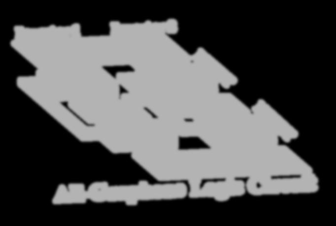


22 2D semiconductor 2D half-metal 2D semi-metal 2D dielectric 2D metal We researchers A future 2D Legoland G D GNRTFET Biosensor G D GNRTFET Inverter 1 Inverter 2 V DD TG P-NDR V DD V in GND BG BG TG N-NDR V out NDR-based RAM V out1 V out2 V in GND All-Graphene Logic Circuit Kaustav Banerjee, UC anta Barbara kaustav@ece.ucsb.edu May 25, 2015, FANEM Workshop 23
Invited Paper. Graphene and Beyond-Graphene 2D Crystals for Next-Generation Green Electronics
 Invited Paper Graphene and Beyond-Graphene 2D Crystals for Next-Generation Green Electronics Jiahao Kang, Wei Cao, Xuejun Xie, Deblina Sarkar, Wei Liu and Kaustav Banerjee* Department of Electrical and
Electronics with 2D Crystals: Scaling extender, or harbinger of new functions?
 Electronics with 2D Crystals: Scaling extender, or harbinger of new functions? 1 st Workshop on Data Abundant Systems Technology Stanford, April 2014 Debdeep Jena (djena@nd.edu) Electrical Engineering,
Carbon Inside: Next-Generation Interconnects for Green Electronics. Kaustav Banerjee
 17 th IEEE Workshop on Signal and Power Integrity, Paris, France, May 12-15, 2013 UC Santa Barbara Carbon Inside: Next-Generation Interconnects for Green Electronics Kaustav Banerjee Department of Electrical
Supporting Information
 Supporting Information Monolithically Integrated Flexible Black Phosphorus Complementary Inverter Circuits Yuanda Liu, and Kah-Wee Ang* Department of Electrical and Computer Engineering National University
2D MBE Activities in Sheffield. I. Farrer, J. Heffernan Electronic and Electrical Engineering The University of Sheffield
 2D MBE Activities in Sheffield I. Farrer, J. Heffernan Electronic and Electrical Engineering The University of Sheffield Outline Motivation Van der Waals crystals The Transition Metal Di-Chalcogenides
FIELD EFFECT TRANSISTORS:
 Chapter 10 FIEL EFFECT TRANITOR: MOFET The following overview gures describe important issues related to the most important electronic device. NUMBER OF ACTIVE EVICE/CHIP MOORE' LAW Gordon Moore, co-founder
L ECE 4211 UConn F. Jain Scaling Laws for NanoFETs Chapter 10 Logic Gate Scaling
 L13 04202017 ECE 4211 UConn F. Jain Scaling Laws for NanoFETs Chapter 10 Logic Gate Scaling Scaling laws: Generalized scaling (GS) p. 610 Design steps p.613 Nanotransistor issues (page 626) Degradation
A final review session will be offered on Thursday, May 10 from 10AM to 12noon in 521 Cory (the Hogan Room).
.") A final review session will be offered on Thursday, May 10 from 10AM to 12noon in 521 Cory (the Hogan Room). The Final Exam will take place from 12:30PM to 3:30PM on Saturday May 12 in 60 Evans.» All of
A final review session will be offered on Thursday, May 10 from 10AM to 12noon in 521 Cory (the Hogan Room). The Final Exam will take place from 12:30PM to 3:30PM on Saturday May 12 in 60 Evans.» All of
Lecture 6: 2D FET Electrostatics
 Lecture 6: 2D FET Electrostatics 2016-02-01 Lecture 6, High Speed Devices 2014 1 Lecture 6: III-V FET DC I - MESFETs Reading Guide: Liu: 323-337 (he mainly focuses on the single heterostructure FET) Jena:
Comparison of Ultra-Thin InAs and InGaAs Quantum Wells and Ultra-Thin-Body Surface-Channel MOSFETs
 Comparison of Ultra-Thin InAs and InGaAs Quantum Wells and Ultra-Thin-Body Surface-Channel MOSFETs Cheng-Ying Huang 1, Sanghoon Lee 1, Evan Wilson 3, Pengyu Long 3, Michael Povolotskyi 3, Varistha Chobpattana
Evaluation of Electronic Characteristics of Double Gate Graphene Nanoribbon Field Effect Transistor for Wide Range of Temperatures
 Evaluation of Electronic Characteristics of Double Gate Graphene Nanoribbon Field Effect Transistor for Wide Range of Temperatures 1 Milad Abtin, 2 Ali Naderi 1 Department of electrical engineering, Masjed
MSE 310/ECE 340: Electrical Properties of Materials Fall 2014 Department of Materials Science and Engineering Boise State University
 MSE 310/ECE 340: Electrical Properties of Materials Fall 2014 Department of Materials Science and Engineering Boise State University Practice Final Exam 1 Read the questions carefully Label all figures
Operating Principles of Vertical Transistors Based on Monolayer Two-Dimensional Semiconductor Heterojunctions
 Operating Principles of Vertical Transistors Based on Monolayer Two-Dimensional Semiconductor Heterojunctions Kai Tak Lam, Gyungseon Seol and Jing Guo Department of Electrical and Computer Engineering,
arxiv: v2 [cond-mat.mtrl-sci] 11 Sep 2016
![arxiv: v2 [cond-mat.mtrl-sci] 11 Sep 2016](/thumbs/73/68883795.jpg "arxiv: v2 [cond-mat.mtrl-sci] 11 Sep 2016") arxiv:1608.05057v2 [cond-mat.mtrl-sci] 11 ep 2016 Transport in vertically stacked hetero-structures from 2D materials Fan Chen, Hesameddin Ilatikhameneh, Yaohua Tan, Daniel Valencia, Gerhard Klimeck and
arxiv:1608.05057v2 [cond-mat.mtrl-sci] 11 ep 2016 Transport in vertically stacked hetero-structures from 2D materials Fan Chen, Hesameddin Ilatikhameneh, Yaohua Tan, Daniel Valencia, Gerhard Klimeck and
MOSFET: Introduction
 E&CE 437 Integrated VLSI Systems MOS Transistor 1 of 30 MOSFET: Introduction Metal oxide semiconductor field effect transistor (MOSFET) or MOS is widely used for implementing digital designs Its major
Effect of the High-k Dielectric/Semiconductor Interface on Electronic Properties in Ultra-thin Channels
 Effect of the High-k Dielectric/Semiconductor Interface on Electronic Properties in Ultra-thin Channels Evan Wilson, Daniel Valencia, Mark J. W. Rodwell, Gerhard Klimeck and Michael Povolotskyi Electrical
Sub-Boltzmann Transistors with Piezoelectric Gate Barriers
 Sub-Boltzmann Transistors with Piezoelectric Gate Barriers Raj Jana, Gregory Snider, Debdeep Jena Electrical Engineering University of Notre Dame 29 Oct, 2013 rjana1@nd.edu Raj Jana, E3S 2013, Berkeley
The Critical Role of Quantum Capacitance in Compact Modeling of Nano-Scaled and Nanoelectronic Devices
 The Critical Role of Quantum Capacitance in Compact Modeling of Nano-Scaled and Nanoelectronic Devices Zhiping Yu and Jinyu Zhang Institute of Microelectronics Tsinghua University, Beijing, China yuzhip@tsinghua.edu.cn
Graphene devices and integration: A primer on challenges
 Graphene devices and integration: A primer on challenges Archana Venugopal (TI) 8 Nov 2016 Acknowledgments: Luigi Colombo (TI) UT Dallas and UT Austin 1 Outline Where we are Issues o Contact resistance
NEM Relay Design for Compact, Ultra-Low-Power Digital Logic Circuits
 NEM Relay Design for Compact, Ultra-Low-Power Digital Logic Circuits T.-J. K. Liu 1, N. Xu 1, I.-R. Chen 1, C. Qian 1, J. Fujiki 2 1 Dept. of Electrical Engineering and Computer Sciences University of
Emerging Interconnect Technologies for CMOS and beyond-cmos Circuits
 Emerging Interconnect Technologies for CMOS and beyond-cmos Circuits Sou-Chi Chang, Rouhollah M. Iraei Vachan Kumar, Ahmet Ceyhan and Azad Naeemi School of Electrical & Computer Engineering Georgia Institute
EE410 vs. Advanced CMOS Structures
 EE410 vs. Advanced CMOS Structures Prof. Krishna S Department of Electrical Engineering S 1 EE410 CMOS Structure P + poly-si N + poly-si Al/Si alloy LPCVD PSG P + P + N + N + PMOS N-substrate NMOS P-well
Contact Engineering of Two-Dimensional Layered Semiconductors beyond Graphene
 Contact Engineering of Two-Dimensional Layered Semiconductors beyond Graphene Zhixian Zhou Department of Physics and Astronomy Wayne State University Detroit, Michigan Outline Introduction Ionic liquid
Quantum Mechanical Simulation for Ultra-thin High-k Gate Dielectrics Metal Oxide Semiconductor Field Effect Transistors
 Mechanical Simulation for Ultra-thin High-k Gate Dielectrics Metal Oxide Semiconductor Field Effect Transistors Shih-Ching Lo 1, Yiming Li 2,3, and Jyun-Hwei Tsai 1 1 National Center for High-Performance
Understanding the effect of n-type and p-type doping in the channel of graphene nanoribbon transistor
 Bull. Mater. Sci., Vol. 39, No. 5, September 2016, pp. 1303 1309. DOI 10.1007/s12034-016-1277-9 c Indian Academy of Sciences. Understanding the effect of n-type and p-type doping in the channel of graphene
Carbon Nanotube Electronics
 Carbon Nanotube Electronics Jeorg Appenzeller, Phaedon Avouris, Vincent Derycke, Stefan Heinz, Richard Martel, Marko Radosavljevic, Jerry Tersoff, Shalom Wind H.-S. Philip Wong hspwong@us.ibm.com IBM T.J.
CHAPTER 5 EFFECT OF GATE ELECTRODE WORK FUNCTION VARIATION ON DC AND AC PARAMETERS IN CONVENTIONAL AND JUNCTIONLESS FINFETS
 98 CHAPTER 5 EFFECT OF GATE ELECTRODE WORK FUNCTION VARIATION ON DC AND AC PARAMETERS IN CONVENTIONAL AND JUNCTIONLESS FINFETS In this chapter, the effect of gate electrode work function variation on DC
Supplementary Figure 2 Photoluminescence in 1L- (black line) and 7L-MoS 2 (red line) of the Figure 1B with illuminated wavelength of 543 nm.
 and 7L-MoS 2 (red line) of the Figure 1B with illuminated wavelength of 543 nm.") PL (normalized) Intensity (arb. u.) 1 1 8 7L-MoS 1L-MoS 6 4 37 38 39 4 41 4 Raman shift (cm -1 ) Supplementary Figure 1 Raman spectra of the Figure 1B at the 1L-MoS area (black line) and 7L-MoS area (red
PL (normalized) Intensity (arb. u.) 1 1 8 7L-MoS 1L-MoS 6 4 37 38 39 4 41 4 Raman shift (cm -1 ) Supplementary Figure 1 Raman spectra of the Figure 1B at the 1L-MoS area (black line) and 7L-MoS area (red
EECS130 Integrated Circuit Devices
 EECS130 Integrated Circuit Devices Professor Ali Javey 10/30/2007 MOSFETs Lecture 4 Reading: Chapter 17, 19 Announcements The next HW set is due on Thursday. Midterm 2 is next week!!!! Threshold and Subthreshold
A Numerical Study of Scaling Issues for Schottky Barrier Carbon Nanotube Transistors
 A Numerical Study of Scaling Issues for Schottky Barrier Carbon Nanotube Transistors Jing Guo, Supriyo Datta and Mark Lundstrom School of Electrical and Computer Engineering, Purdue University, West Lafayette,
R. Ludwig and G. Bogdanov RF Circuit Design: Theory and Applications 2 nd edition. Figures for Chapter 6
 R. Ludwig and G. Bogdanov RF Circuit Design: Theory and Applications 2 nd edition Figures for Chapter 6 Free electron Conduction band Hole W g W C Forbidden Band or Bandgap W V Electron energy Hole Valence
Lecture 15 OUTLINE. MOSFET structure & operation (qualitative) Review of electrostatics The (N)MOS capacitor
 Review of electrostatics The (N)MOS capacitor") Lecture 15 OUTLINE MOSFET structure & operation (qualitative) Review of electrostatics The (N)MOS capacitor Electrostatics t ti Charge vs. voltage characteristic Reading: Chapter 6.1 6.2.1 EE105 Fall 2007
Lecture 15 OUTLINE MOSFET structure & operation (qualitative) Review of electrostatics The (N)MOS capacitor Electrostatics t ti Charge vs. voltage characteristic Reading: Chapter 6.1 6.2.1 EE105 Fall 2007
(a) (b) Supplementary Figure 1. (a) (b) (a) Supplementary Figure 2. (a) (b) (c) (d) (e)
 (b) Supplementary Figure 1. (a) (b) (a) Supplementary Figure 2. (a) (b) (c) (d) (e)") (a) (b) Supplementary Figure 1. (a) An AFM image of the device after the formation of the contact electrodes and the top gate dielectric Al 2 O 3. (b) A line scan performed along the white dashed line
(a) (b) Supplementary Figure 1. (a) An AFM image of the device after the formation of the contact electrodes and the top gate dielectric Al 2 O 3. (b) A line scan performed along the white dashed line
Low Frequency Noise in MoS 2 Negative Capacitance Field-effect Transistor
 Low Frequency Noise in MoS Negative Capacitance Field-effect Transistor Sami Alghamdi, Mengwei Si, Lingming Yang, and Peide D. Ye* School of Electrical and Computer Engineering Purdue University West Lafayette,
A Physically Based Compact I V Model for Monolayer TMDC Channel MOSFET and DMFET Biosensor
 1 A Physically Based Compact I V Model for Monolayer TMDC Channel MOSFET and DMFET Biosensor Ehsanur Rahman 1$**, Abir Shadman 1$, Imtiaz Ahmed 1, Saeed Uz Zaman Khan 1 and Quazi D. M. Khosru 1 1 Department
ECE 342 Electronic Circuits. 3. MOS Transistors
 ECE 342 Electronic Circuits 3. MOS Transistors Jose E. Schutt-Aine Electrical & Computer Engineering University of Illinois jschutt@emlab.uiuc.edu 1 NMOS Transistor Typically L = 0.1 to 3 m, W = 0.2 to
Metallic: 2n 1. +n 2. =3q Armchair structure always metallic = 2
 Properties of CNT d = 2.46 n 2 2 1 + n1n2 + n2 2π Metallic: 2n 1 +n 2 =3q Armchair structure always metallic a) Graphite Valence(π) and Conduction(π*) states touch at six points(fermi points) Carbon Nanotube:
Drift-diffusion model for single layer transition metal dichalcogenide field-effect transistors
 Drift-diffusion model for single layer transition metal dichalcogenide field-effect transistors David Jiménez Departament d'enginyeria Electrònica, Escola d'enginyeria, Universitat Autònoma de Barcelona,
Lecture 04 Review of MOSFET
 ECE 541/ME 541 Microelectronic Fabrication Techniques Lecture 04 Review of MOSFET Zheng Yang (ERF 3017, email: yangzhen@uic.edu) What is a Transistor? A Switch! An MOS Transistor V GS V T V GS S Ron D
Timing Simulation of 45 nm Technology and Analysis of Gate Tunneling Currents in 90, 65, 45, and 32 nm Technologies
 1 Timing Simulation of 45 nm Technology and Analysis of Gate Tunneling Currents in 90, 65, 45, and 32 nm Technologies Steven P. Surgnier Abstract A timing simulation is presented for a MOSFET implemented
ESE 570: Digital Integrated Circuits and VLSI Fundamentals
 ESE 570: Digital Integrated Circuits and VLSI Fundamentals Lec 4: January 23, 2018 MOS Transistor Theory, MOS Model Penn ESE 570 Spring 2018 Khanna Lecture Outline! CMOS Process Enhancements! Semiconductor
Fermi Level Pinning at Electrical Metal Contacts. of Monolayer Molybdenum Dichalcogenides
 Supporting information Fermi Level Pinning at Electrical Metal Contacts of Monolayer Molybdenum Dichalcogenides Changsik Kim 1,, Inyong Moon 1,, Daeyeong Lee 1, Min Sup Choi 1, Faisal Ahmed 1,2, Seunggeol
Microelectronics Part 1: Main CMOS circuits design rules
 GBM8320 Dispositifs Médicaux telligents Microelectronics Part 1: Main CMOS circuits design rules Mohamad Sawan et al. Laboratoire de neurotechnologies Polystim! http://www.cours.polymtl.ca/gbm8320/! med-amine.miled@polymtl.ca!
Future Trends in Microelectronics Impact on Detector Readout. Paul O Connor
 Future Trends in Microelectronics Impact on Detector Readout Paul O Connor Outline CMOS Technology Scaling Analog Circuits Radiation Effects Cost Detector Development Symposium Paul O'Connor BNL April
Scaling Issues in Planar FET: Dual Gate FET and FinFETs
 Scaling Issues in Planar FET: Dual Gate FET and FinFETs Lecture 12 Dr. Amr Bayoumi Fall 2014 Advanced Devices (EC760) Arab Academy for Science and Technology - Cairo 1 Outline Scaling Issues for Planar
Monolayer Semiconductors
 Monolayer Semiconductors Gilbert Arias California State University San Bernardino University of Washington INT REU, 2013 Advisor: Xiaodong Xu (Dated: August 24, 2013) Abstract Silicon may be unable to
Graphene Varactors as a Sensing Platform for Biotechnology Applications
 Graphene Varactors as a Sensing Platform for Biotechnology Applications Steven J. Koester 1, Eric J. Olson 1, David Deen 1, Yao Zhang 1, Mona A. Ebrish 1, Rui Ma 1, Nazila Haratipour 1, Philippe Buhlmann
MOS Transistors. Prof. Krishna Saraswat. Department of Electrical Engineering Stanford University Stanford, CA
 MOS Transistors Prof. Krishna Saraswat Department of Electrical Engineering S Stanford, CA 94305 saraswat@stanford.edu 1 1930: Patent on the Field-Effect Transistor! Julius Lilienfeld filed a patent describing
Investigation of the Dimension Effects of Sub-30nm Multiple-Gate SOI MOSFETs by TCAD Simulation
 Microelectronics and olid tate Electronics 212, 1(3): 64-68 OI: 1.5923/j.msse.21224.3 Investigation of the imension Effects of ub-3nm Multiple-ate OI MOFETs by TCA imulation Keng-Ming Liu *, Yung-Yu Hsieh
Graphene Novel Material for Nanoelectronics
 Graphene Novel Material for Nanoelectronics Shintaro Sato Naoki Harada Daiyu Kondo Mari Ohfuchi (Manuscript received May 12, 2009) Graphene is a flat monolayer of carbon atoms with a two-dimensional honeycomb
SCHOTTKY BARRIER MOSFET DEVICE PHYSICS FOR CRYOGENIC APPLICATIONS
 CHOTTKY BARRIER FET DEVICE PHYIC FOR CRYOGENIC APPLICATION Mike chwarz, Laurie E. Calvet, John P. nyder, Tillmann Krauss, Udo chwalke, Alexander Kloes cope OI and Multi-Gate FETs Dresden ept.3, 2018 New
Nanometer Transistors and Their Models. Jan M. Rabaey
 Nanometer Transistors and Their Models Jan M. Rabaey Chapter Outline Nanometer transistor behavior and models Sub-threshold currents and leakage Variability Device and technology innovations Nanometer
Quantum Phenomena & Nanotechnology (4B5)
") Quantum Phenomena & Nanotechnology (4B5) The 2-dimensional electron gas (2DEG), Resonant Tunneling diodes, Hot electron transistors Lecture 11 In this lecture, we are going to look at 2-dimensional electron
Quantum Phenomena & Nanotechnology (4B5) The 2-dimensional electron gas (2DEG), Resonant Tunneling diodes, Hot electron transistors Lecture 11 In this lecture, we are going to look at 2-dimensional electron
How a single defect can affect silicon nano-devices. Ted Thorbeck
 How a single defect can affect silicon nano-devices Ted Thorbeck tedt@nist.gov The Big Idea As MOS-FETs continue to shrink, single atomic scale defects are beginning to affect device performance Gate Source
Choice of V t and Gate Doping Type
 Choice of V t and Gate Doping Type To make circuit design easier, it is routine to set V t at a small positive value, e.g., 0.4 V, so that, at V g = 0, the transistor does not have an inversion layer and
This article has been accepted and published on J-STAGE in advance of copyediting. Content is final as presented.
 This article has been accepted and published on J-STAGE in advance of copyediting. Content is final as presented. References IEICE Electronics Express, Vol.* No.*,*-* Effects of Gamma-ray radiation on
OMEN an atomistic and full-band quantum transport simulator for post-cmos nanodevices
 Purdue University Purdue e-pubs Other Nanotechnology Publications Birck Nanotechnology Center 8-18-28 OMEN an atomistic and full-band quantum transport simulator for post-cmos nanodevices Mathieu Luisier
I-V characteristics model for Carbon Nanotube Field Effect Transistors
 International Journal of Engineering & Technology IJET-IJENS Vol:14 No:04 33 I-V characteristics model for Carbon Nanotube Field Effect Transistors Rebiha Marki, Chérifa Azizi and Mourad Zaabat. Abstract--
Electrostatics of Nanowire Transistors
 Electrostatics of Nanowire Transistors Jing Guo, Jing Wang, Eric Polizzi, Supriyo Datta and Mark Lundstrom School of Electrical and Computer Engineering Purdue University, West Lafayette, IN, 47907 ABSTRACTS
Influence of structural and doping parameter variations on Si and Si 1 x Ge x double gate tunnel FETs: An analysis for RF performance enhancement
 Pramana J. Phys. (2018) 91:2 https://doi.org/10.1007/s12043-018-1577-2 Indian Academy of Sciences Influence of structural and doping parameter variations on Si and Si 1 x Ge x double gate tunnel FETs:
Lecture 2 Thin Film Transistors
 Lecture 2 Thin Film Transistors 1/60 Announcements Homework 1/4: Will be online after the Lecture on Tuesday October 2 nd. Total of 25 marks. Each homework contributes an equal weight. All homework contributes
Performance Analysis of Ultra-Scaled InAs HEMTs
 Purdue University Purdue e-pubs Birck and NCN Publications Birck Nanotechnology Center 2009 Performance Analysis of Ultra-Scaled InAs HEMTs Neerav Kharche Birck Nanotechnology Center and Purdue University,
Metal Semiconductor Contacts
 Metal Semiconductor Contacts The investigation of rectification in metal-semiconductor contacts was first described by Braun [33-35], who discovered in 1874 the asymmetric nature of electrical conduction
Field-Effect (FET) transistors
 transistors") Field-Effect (FET) transistors References: Barbow (Chapter 8), Rizzoni (chapters 8 & 9) In a field-effect transistor (FET), the width of a conducting channel in a semiconductor and, therefore, its current-carrying
Field-Effect (FET) transistors References: Barbow (Chapter 8), Rizzoni (chapters 8 & 9) In a field-effect transistor (FET), the width of a conducting channel in a semiconductor and, therefore, its current-carrying
ALD high-k and higher-k integration on GaAs
 ALD high-k and higher-k integration on GaAs Ozhan Koybasi 1), Min Xu 1), Yiqun Liu 2), Jun-Jieh Wang 2), Roy G. Gordon 2), and Peide D. Ye 1)* 1) School of Electrical and Computer Engineering, Purdue University,
Chun Yung Sung Science and Technology Strategy Department IBM T.J. Watson Research Center Yorktown, NY, USA
 51. Reconfigurable Multi-Function Logic Based on Graphene P-N Junctions Sansiri Tanachutiwat, Ji Ung Lee, and Wei Wang College of Nanoscale Science and Engineering University at Albany, State University
Stretching the Barriers An analysis of MOSFET Scaling. Presenters (in order) Zeinab Mousavi Stephanie Teich-McGoldrick Aseem Jain Jaspreet Wadhwa
 Zeinab Mousavi Stephanie Teich-McGoldrick Aseem Jain Jaspreet Wadhwa") Stretching the Barriers An analysis of MOSFET Scaling Presenters (in order) Zeinab Mousavi Stephanie Teich-McGoldrick Aseem Jain Jaspreet Wadhwa Why Small? Higher Current Lower Gate Capacitance Higher
Stretching the Barriers An analysis of MOSFET Scaling Presenters (in order) Zeinab Mousavi Stephanie Teich-McGoldrick Aseem Jain Jaspreet Wadhwa Why Small? Higher Current Lower Gate Capacitance Higher
Lecture 5: CMOS Transistor Theory
 Lecture 5: CMOS Transistor Theory Slides courtesy of Deming Chen Slides based on the initial set from David Harris CMOS VLSI Design Outline q q q q q q q Introduction MOS Capacitor nmos I-V Characteristics
Solid State Device Fundamentals
 Solid State Device Fundamentals ENS 345 Lecture Course by Alexander M. Zaitsev alexander.zaitsev@csi.cuny.edu Tel: 718 982 2812 Office 4N101b 1 Outline - Goals of the course. What is electronic device?
2D-2D tunneling field effect transistors using
 2D-2D tunneling field effect transistors using WSe 2 /SnSe 2 heterostructures Tania Roy, 1,2,3 Mahmut Tosun, 1,2,3 Mark Hettick, 1,2,3, Geun Ho Ahn, 1,2,3 Chenming Hu 1, and Ali Javey 1,2,3, 1 Electrical
The Devices: MOS Transistors
 The Devices: MOS Transistors References: Semiconductor Device Fundamentals, R. F. Pierret, Addison-Wesley Digital Integrated Circuits: A Design Perspective, J. Rabaey et.al. Prentice Hall NMOS Transistor
Tunnel-FET: bridging the gap between prediction and experiment through calibration
 Tunnel-FET: bridging the gap between prediction and experiment through calibration Anne Verhulst Quentin Smets, Jasper Bizindavyi, Mazhar Mohammed, Devin Verreck, Salim El Kazzi, Alireza Alian, Yves Mols,
Directions for simulation of beyond-cmos devices. Dmitri Nikonov, George Bourianoff, Mark Stettler
 Directions for simulation of beyond-cmos devices Dmitri Nikonov, George Bourianoff, Mark Stettler Outline Challenges and responses in nanoelectronic simulation Limits for electronic devices and motivation
A Multi-Gate CMOS Compact Model BSIMMG
 A Multi-Gate CMOS Compact Model BSIMMG Darsen Lu, Sriramkumar Venugopalan, Tanvir Morshed, Yogesh Singh Chauhan, Chung-Hsun Lin, Mohan Dunga, Ali Niknejad and Chenming Hu University of California, Berkeley
III-V CMOS: What have we learned from HEMTs? J. A. del Alamo, D.-H. Kim 1, T.-W. Kim, D. Jin, and D. A. Antoniadis
 III-V CMOS: What have we learned from HEMTs? J. A. del Alamo, D.-H. Kim 1, T.-W. Kim, D. Jin, and D. A. Antoniadis Microsystems Technology Laboratories, MIT 1 presently with Teledyne Scientific 23rd International
FLCC Seminar. Spacer Lithography for Reduced Variability in MOSFET Performance
 1 Seminar Spacer Lithography for Reduced Variability in MOSFET Performance Prof. Tsu-Jae King Liu Electrical Engineering & Computer Sciences Dept. University of California at Berkeley Graduate Student:
Modeling and Performance analysis of Metallic CNT Interconnects for VLSI Applications
 IOSR Journal of Electronics and Communication Engineering (IOSR-JECE) e-issn: 2278-2834, p- ISSN: 2278-8735. Volume 4, Issue 6 (Jan. - Feb. 2013), PP 32-36 Modeling and Performance analysis of Metallic
Fundamentals of the Metal Oxide Semiconductor Field-Effect Transistor
 Triode Working FET Fundamentals of the Metal Oxide Semiconductor Field-Effect Transistor The characteristics of energy bands as a function of applied voltage. Surface inversion. The expression for the
M R S Internet Journal of Nitride Semiconductor Research
 Page 1 of 6 M R S Internet Journal of Nitride Semiconductor Research Volume 9, Article 7 The Ambient Temperature Effect on Current-Voltage Characteristics of Surface-Passivated GaN-Based Field-Effect Transistors
Index. buried oxide 35, 44 51, 89, 238 buried channel 56
 Index A acceptor 275 accumulation layer 35, 45, 57 activation energy 157 Auger electron spectroscopy (AES) 90 anode 44, 46, 55 9, 64, 182 anode current 45, 49, 65, 77, 106, 128 anode voltage 45, 52, 65,
MOS Transistor I-V Characteristics and Parasitics
 ECEN454 Digital Integrated Circuit Design MOS Transistor I-V Characteristics and Parasitics ECEN 454 Facts about Transistors So far, we have treated transistors as ideal switches An ON transistor passes
ESE 570: Digital Integrated Circuits and VLSI Fundamentals
 ESE 570: Digital Integrated Circuits and VLSI Fundamentals Lec 4: January 29, 2019 MOS Transistor Theory, MOS Model Penn ESE 570 Spring 2019 Khanna Lecture Outline! CMOS Process Enhancements! Semiconductor
Ultra-low-voltage bilayer graphene tunnel FET
 Ultra-low-voltage bilayer graphene tunnel FET 1 arxiv:0906.1254v1 [cond-mat.mes-hall] 6 Jun 2009 Gianluca Fiori, Giuseppe Iannaccone Dipartimento di Ingegneria dell Informazione : Elettronica, Informatica,
Bridging the Gap: Black Phosphorus for Electronics and Photonics
 IBM Thomas J. Watson Research Center Bridging the Gap: Black Phosphorus for Electronics and Photonics Fengnian Xia Department of Electrical Engineering Yale University, New Haven CT 06511 Email: fengnian.ia@yale.edu
Classification of Solids
 Classification of Solids Classification by conductivity, which is related to the band structure: (Filled bands are shown dark; D(E) = Density of states) Class Electron Density Density of States D(E) Examples
Erik Lind
 High-Speed Devices, 2011 Erik Lind (Erik.Lind@ftf.lth.se) Course consists of: 30 h Lectures (H322, and Fys B check schedule) 8h Excercises 2x2h+4h Lab Excercises (2 Computer simulations, 4 RF measurment
ECE 546 Lecture 10 MOS Transistors
 ECE 546 Lecture 10 MOS Transistors Spring 2018 Jose E. Schutt-Aine Electrical & Computer Engineering University of Illinois jesa@illinois.edu NMOS Transistor NMOS Transistor N-Channel MOSFET Built on p-type
Future trends in radiation hard electronics
 Future trends in radiation hard electronics F. Faccio CERN, Geneva, Switzerland Outline Radiation effects in CMOS technologies Deep submicron CMOS for radiation environments What is the future going to
Physics in two dimensions in the lab
 Physics in two dimensions in the lab Nanodevice Physics Lab David Cobden PAB 308 Collaborators at UW Oscar Vilches (Low Temperature Lab) Xiaodong Xu (Nanoscale Optoelectronics Lab) Jiun Haw Chu (Quantum
Semiconductor Memories
 Semiconductor References: Adapted from: Digital Integrated Circuits: A Design Perspective, J. Rabaey UCB Principles of CMOS VLSI Design: A Systems Perspective, 2nd Ed., N. H. E. Weste and K. Eshraghian
Analysis of Band-to-band. Tunneling Structures. Title of Talk. Dimitri Antoniadis and Judy Hoyt (PIs) Jamie Teherani and Tao Yu (Students) 8/21/2012
 Jamie Teherani and Tao Yu (Students) 8/21/2012") 1 Analysis of Band-to-band Title of Talk Tunneling Structures Dimitri Antoniadis and Judy Hoyt (PIs) Jamie Teherani and Tao Yu (Students) 8/21/2012 A Science & Technology Center Vertical Type-II TFET Structure
1 Analysis of Band-to-band Title of Talk Tunneling Structures Dimitri Antoniadis and Judy Hoyt (PIs) Jamie Teherani and Tao Yu (Students) 8/21/2012 A Science & Technology Center Vertical Type-II TFET Structure
ECE 497 JS Lecture - 12 Device Technologies
 ECE 497 JS Lecture - 12 Device Technologies Spring 2004 Jose E. Schutt-Aine Electrical & Computer Engineering University of Illinois jose@emlab.uiuc.edu 1 NMOS Transistor 2 ρ Source channel charge density
MOS Transistor Theory
 MOS Transistor Theory So far, we have viewed a MOS transistor as an ideal switch (digital operation) Reality: less than ideal EE 261 Krish Chakrabarty 1 Introduction So far, we have treated transistors
SUPPLEMENTARY INFORMATION
 SUPPLEMENTARY INFORMATION doi:10.1038/nature15387 S1. ADVANTAGES OF D MATERIALS for ULTRA SHORT-CHANNEL FIELD-EFFECT TRANSISTORS In a field-effect-transistor (Fig. S1(a)), current flows through a semiconducting
Analysis of InAs Vertical and Lateral Band-to-Band Tunneling. Transistors: Leveraging Vertical Tunneling for Improved Performance
 Analysis of InAs Vertical and Lateral Band-to-Band Tunneling Transistors: Leveraging Vertical Tunneling for Improved Performance Kartik Ganapathi, Youngki Yoon and Sayeef Salahuddin a) Department of Electrical
Scaling of MOS Circuits. 4. International Technology Roadmap for Semiconductors (ITRS) 6. Scaling factors for device parameters
 6. Scaling factors for device parameters") 1 Scaling of MOS Circuits CONTENTS 1. What is scaling?. Why scaling? 3. Figure(s) of Merit (FoM) for scaling 4. International Technology Roadmap for Semiconductors (ITRS) 5. Scaling models 6. Scaling factors
1 Scaling of MOS Circuits CONTENTS 1. What is scaling?. Why scaling? 3. Figure(s) of Merit (FoM) for scaling 4. International Technology Roadmap for Semiconductors (ITRS) 5. Scaling models 6. Scaling factors
Impact of intrinsic deformations on the negative differential resistance of monolayer MoS 2 ultrashort channel MOSFET
 Impact of intrinsic deformations on the negative differential resistance of monolayer MoS 2 ultrashort channel MOSFET Amretashis Sengupta*, Santanu Mahapatra Nano-Scale Device Research Laboratory, Dept.
Device Performance Analysis of Graphene Nanoribbon Field-Effect Transistor with Rare- Earth Oxide (La 2 O 3 ) Based High-k Gate Dielectric
 Based High-k Gate Dielectric") Device Performance Analysis of Graphene Nanoribbon Field-Effect Transistor with Rare- Earth Oxide (La 2 O 3 ) Based High-k Gate Dielectric M. K. Bera 1, S. P. Pandey 2, A. K. Sharma 3, D. K. Tyagi 4, R.
Device Performance Analysis of Graphene Nanoribbon Field-Effect Transistor with Rare- Earth Oxide (La 2 O 3 ) Based High-k Gate Dielectric M. K. Bera 1, S. P. Pandey 2, A. K. Sharma 3, D. K. Tyagi 4, R.
Modeling of the Substrate Current and Characterization of Traps in MOSFETs under Sub-Bandgap Photonic Excitation
 Journal of the Korean Physical Society, Vol. 45, No. 5, November 2004, pp. 1283 1287 Modeling of the Substrate Current and Characterization of Traps in MOSFETs under Sub-Bandgap Photonic Excitation I.
Doping-Free Fabrication of Carbon Nanotube Based Ballistic CMOS Devices and Circuits
 Doping-Free Fabrication of Carbon Nanotube Based Ballistic CMOS Devices and Circuits NANO LETTERS 2007 Vol. 7, No. 12 3603-3607 Zhiyong Zhang, Xuelei Liang,*, Sheng Wang, Kun Yao, Youfan Hu, Yuzhen Zhu,