Operating Principles of Vertical Transistors Based on Monolayer Two-Dimensional Semiconductor Heterojunctions
|
|
|
- Victor Eugene Hancock
- 5 years ago
- Views:
Transcription
1 Operating Principles of Vertical Transistors Based on Monolayer Two-Dimensional Semiconductor Heterojunctions Kai Tak Lam, Gyungseon Seol and Jing Guo Department of Electrical and Computer Engineering, University of Florida, Gainesville, FL ABSTRACT A vertical transistor based on a double gated, atomically thin heterojunction is theoretically examined. Both p-type and n-type transistor operations can be conveniently achieved by using one of the two gates as the switching gate. The transistor shows excellent saturation of output I- V characteristics due to drain-induced depletion and lack of tunneling barrier layers. The subthreshold slope could be below the thermionic limit due to band filtering as the switching mechanism. The atomically thin vertical PN heterojunction can be electrostatically modulated from a type II heterojunction to a broken bandgap alignment, which is preferred for maximizing the on-current. 1
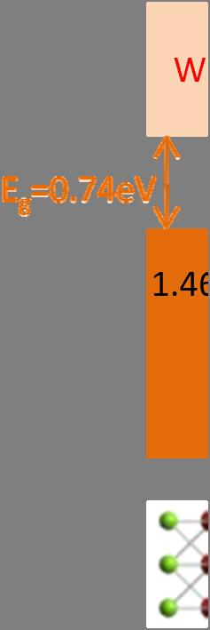
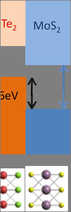
2 Two-dimensional (2D) layered dichalcogenide materials, which offer a bandgap that is absent in graphene, have attracted extensive research interest for potential electronic device applications[1]. Vertical tunneling field effect transistors (FETs), which uses graphene as the source and drain contacts, and sandwiched BN or 2D dichacolgenide layers as the tunneling barrier, have been experimentally fabricated and theoretically examined [2-6]. Several orders of magnitude in on-off current ratio have been achieved. The on-current, however, is limited by the tunneling barrier and the output I-V characteristic lacks a saturation region [2], which is a necessary requirement for many digital and analog circuit applications. On the other hand, atomically thin PN heterojunctions between monolayer dichacolgenide materials have been experimentally demonstrated, which show rectifying I-V characteristics and photocurrent modulated by a gate bias [7]. Recently, two-dimensional heterojunction interlayer tunneling FETs have been theoretically examined [8], and a study on their transfer characteristics suggested that this tunneling FETs could achieve ultrasteep subthreshold slope. In this work, we theoretically model a vertical FET formed with a heterojunction between a monolayer N type and P type 2D material modulated by double gates. The output characteristics of the heterojunction FETs show excellent saturation due to drain induced depletion. Furthermore, without any tunneling barrier layer between the N type and P type materials, the transistor is expected to deliver a larger on-current compared to those with tunneling barrier layers. Both P type and N type operations of the transistor, which are crucial for potential CMOS and analogue applications of the device, can be achieved by properly choosing a switching gate. Electrostatic modulation of atomically thin PN heterojunctions is also studied. The modeled device structure is shown in Fig. 1. The atomically thin heterojunction is formed between WTe 2 and MoS 2 monolayers, which are modulated by top and bottom gates with 2
3 a gate insulator thickness of t ox =3nm and dielectric constant of κ=20. The affinity and bandgap of monolayer MX 2 dichacolgenide materials have been studied before. As shown in Fig. 1(b), the band alignment in the absence of gating is determined according to the ab intio simulation results reported in Ref. [9], and the qualitative conclusions are insensitive to the uncertainty of the equilibrium band alignment. We focus our attention on the intrinsic properties of the vertical field-effect transistor (FET) formed by the double gated monolayer heterojunction, and assume that the MoS 2 and WTe 2 out of the gating region are sufficiently heavily doped [10, 11], so that the extension regions do not play a role in intrinsic vertical transistor switching. Self-consistent electrostatics plays an important role in transistor characteristics. In this work, the carrier statistics equations in WTe 2 and MoS 2 monolayers with Fermi levels split by the applied voltage are solved self-consistently with Poisson equation in the form of a capacitance model. The approach of calculating the self-consistent electrostatic potential is same as what was described before in vertical tunneling transistors [5]. After the self-consistent electrostatic potential is obtained, the source-drain current is computed as the interlayer current by using the Landauer-Buttiker formula [12], = ( ) ( ) ( ),, (1) where g s is the spin degeneracy factor,, ( ) is the Fermi Dirac distribution function, and ( ) is the interlayer transmission between the wave state with a wave vectors of in the top layer and that in the bottom layer with a wave vector of. The interlayer transmission can be computed as follows if the interlayer coupling is weak compared to intralayer binding [13], ( ) = ( ) ( ), (2) 3
4 where is the matrix element of the scattering potential between the wave states. The spectral function is, ( ) =2,,, (3) where,, is the E-k relation of the top and bottom layer. Integrating Eq. (1) over energy results in the following expression [8, 14], = ħ, ( ) ( ) ( ), (4) and the current density is = ħ ( ) ( ) ( ) ( ) ( ), (5) where S is the area of the monolayer heterojunction. The following argument can be made on why the current density J is independent of area S. With one interlayer scatterer, the potential matrix element scales as 1/. In the presence of N uncorrelated scatterers, scales as =, where is the area density of interlayer scatterers., therefore, is independent of the area and is proportional to. Interlayer scattering events play an important role in conserving momentum and energy in interlayer transport. The exact mechanisms of interlayer scattering are unclear, which could be sample-dependent and due to charge impurities, disorders and etc. The uncertainty hinders first principle calculation of the matrix element, which can be a fitting parameter from experimental data. Approximations, however, can be made on the matrix element to facilitate study of the device characteristics. If the in-plane component of the interlayer scattering potential is a short range potential and can be approximated by a delta function, its Fourier component is 4
5 wave vector independent, =. In this case, Eq. (5) can be simplified to a form proportional to the product of density of states (DOS) [2, 3], = ħ ( ) ( ) ( ) ( ), (6) where, ( ) is the DOS of the top and bottom layer without spin degeneracy. The current density can also be expressed as, = ( )( ) ( ) ( ) ( ), (7) where the interlayer transport rates of the carriers τ t(b) in the top (bottom) layer is determined by an expression like the Fermi's golden rule, ( ) = ħ ( )( ). (8) Furthermore, to examine the effect of wavevector dependent interlayer scattering potential, the matrix element in the form of [8] = / /, (9) is used in the calculation of current in Eqs. (1) and (2), where is a constant in the unit of ev, the wavevector =, and is a parameter in the unit of length. The spectral function in Eq. (3) is under the approximation of no broadening, which requires high quality of semiconductors and weak interlayer coupling. Introducing a finite broadening results in the following expression,, ( ) =2, (10),,, 5
6 which leads to bandgap states and describes the finite carrier lifetime due to interlayer coupling and disorder scattering. The impact on I-V characteristics can be assessed by using Eq. (9) in the calculation of current. In order to understand the switching mechanism of the vertical monolayer heterojunction FET, we first examine the band profiles at the off and on states, as shown in Fig. 2. The top gate voltage is fixed at V TG =-0.5 V, which results in p-type electrostatic doping of the WTe 2 and the Fermi level of the top layer E Ft below the valence band of WTe 2. At a low bottom gate voltage of V BG =0V, the carrier density in the MoS 2 layer is low, and the Fermi levels of both the top and bottom layers, E Ft and E Fb, are in the bandgap of MoS 2, and the source-drain current is blocked by the MoS 2 bandgap. As the bottom gate voltage increases, the conduction band edge of MoS 2 moves below the valence band edge and the Fermi level of WTe 2, which results in an on state as shown in Fig. 2b. This band filtering mechanism is responsible for the switching of the vertical monolayer heterojunction FET. The switching mechanism above shares similarity with the band-to-band tunneling FETs, which can offer ultrasteep subthreshold slope below the thermionic limit of 60mV/dec at room temperature[15]. Important difference, however, exists. Both the n-type and p-type semiconductor layers in the heterojuction FET are only monolayer thick, which enables effective electrostatic modulation of the heterojunction interface. The top and bottom gates directly modulate all atoms at the interface which provides advantages in terms of device operation. For example, the on-current of a band-to-band tunneling FET is often limited by band-to-band tunneling, and a broken bandgap heterojunction is preferred but difficult to achieve. For the vertical monolayer heterojunction FET, electrostatic modulation of the heterojunction interface can be so effective that the interface can be modulated from a type II heterojunction at the off 6
7 state to a broken bandgap heterojunction at the on state, as shown in Fig. 2(b), which is preferred for maximizing the on-current. The switching I-V characteristics of the vertical heterojunction FETs are shown in Fig. 3. By fixing the bottom gate voltage to electrostatically dope the MoS 2 layer to n-type, p-type transistor switching is achieved by using the top gate as the switching gate. On the other hand, by using the bottom gate as the switching gate, n-type switching is achieved. Both n-type and p-type transistor characteristics, which are crucial for CMOS applications, can be conveniently achieved by choosing one of the two gates as the switching gate. Figure 3 also shows that due to the switching mechanism of band filtering, the subthreshold slope could be very steep and is limited by bandgap states, as discussed before in 2D semiconductor interlayer tunneling FETs [8]. The minimal leakage current shows different trends for p-type operation and n-type operation due to the following reason. The minimal leakage current is limited by thermionic emission in the conduction band of WTe 2 and the valence band of MoS 2. Because of the much smaller bandgap of WTe 2, thermionic emission in the conduction band of WTe 2 dominates. For n-type transistor operation in Fig. 3(b), the WTe 2 layer, which is grounded, acts as the source, whose Fermi level remains relatively constant to its conduction band edge. As a result, the minimal leakage current is insensitive to the applied drain voltage on MoS 2. For p-type transistor operation, the drain voltage is applied on the WTe 2 layer and as the drain voltage increases, the WTe 2 Fermi level moves closer to the conduction band edge, which results in an increase of the minimal leakage current, as shown in Fig. 3(a). Tunneling barrier material layers, such as layers of BN or MoS 2, were inserted between the source and drain graphene contact layers in previously studied tunneling FETs [2-6, 8]. However, 7
8 the tunneling layer, which is necessary to reduce the leakage current when graphene or metal source and drain contacts are used, restricts the on-current performance. Furthermore, the output I-V characteristics do not saturate, which severely limits the potential application in digital and analog electronics. By using a gated semiconductor PN heterojunction, no tunneling barrier layer is needed in the modeled transistor, resulting in a larger on-current. Furthermore, the output I-V characteristics of the heterojunction FETs show excellent saturation behavior as shown in Fig. 4(a). The saturation of the drain current can be explained by drain-induced depletion of the drain monolayer. As shown in Fig. 4(b), when the drain voltage increases, its Fermi level moves into the bandgap region, and the drain layer becomes depleted. The charge density and band edge in the drain monolayer are insensitive to further increase of the drain voltage, and the source-drain current saturates. The above I-V characteristics are calculated based on Eq. (6), without considering bandgap states. What if the interlayer scattering potential is wavevector dependent and bandgap states are induced by broadening? To include these effects, we compute the device I-V characteristics using Eq. (1), with the wavevector dependent matrix element described in Eq. (9) and broadened spectral function described in Eq. (10). While the qualitative conclusions of both n-type and p- type operations, as well as saturation of the output I-V characteristics, remain the same, the bandgap states due to broadening have a considerable effect on the off-current and the subthreshold slope. As shown in Fig. 5, the off-current increases proportionally with the broadening due to the bandgap states, and the current above the threshold is insensitive to a small value of broadening. The subthreshold slope could still be below the thermionic limit if the broadening is small. The leakage current, however, is limited by the bandgap states. 8
9 In summary, electrostatic modulability of a monolayer vertical heterojunction is advantageous for monolayer heterojunction transistors. Properly chosen 2D monolayer materials can form type II heterojunction band alignment, which blocks the source-drain current by the semiconductor bandgaps at the off state, and electrostatic gating could lead to broken bandgap alignment at the on state. The atomic layer structure ensures that all atoms at the interface are efficiently modulated by electrostatic gating. A double gate configuration allows both n-type and p-type operations by using one of the two gates as the switching gate. The output I-V characteristics saturate due to drain induced depletion of the monolayer. The authors are indebted to Prof. P. Kim of Columbia University for extensive technical discussions. This works was supported by NSF. 9
10 REFERENCES [1] Q. H. Wang, K. Kalantar-Zadeh, A. Kis, J. N. Coleman, and M. S. Strano, "Electronics and optoelectronics of two-dimensional transition metal dichalcogenides," Nature Nanotechnology, vol. 7, pp , Nov [2] L. Britnell, R. V. Gorbachev, R. Jalil, B. D. Belle, F. Schedin, A. Mishchenko, T. Georgiou, M. I. Katsnelson, L. Eaves, S. V. Morozov, N. M. R. Peres, J. Leist, A. K. Geim, K. S. Novoselov, et al., "Field-Effect Tunneling Transistor Based on Vertical Graphene Heterostructures," Science, vol. 335, pp , Feb [3] T. Georgiou, R. Jalil, B. D. Belle, L. Britnell, R. V. Gorbachev, S. V. Morozov, Y. J. Kim, A. Gholinia, S. J. Haigh, O. Makarovsky, L. Eaves, L. A. Ponomarenko, A. K. Geim, K. S. Novoselov, et al., "Vertical field-effect transistor based on graphene-ws2 heterostructures for flexible and transparent electronics," Nature Nanotechnology, vol. 8, pp , Feb [4] W. J. Yu, Z. Li, H. L. Zhou, Y. Chen, Y. Wang, Y. Huang, and X. F. Duan, "Vertically stacked multiheterostructures of layered materials for logic transistors and complementary inverters," Nature Materials, vol. 12, pp , Mar [5] S. B. Kumar, G. Seol, and J. Guo, "Modeling of a vertical tunneling graphene heterojunction fieldeffect transistor," Applied Physics Letters, vol. 101, Jul [6] G. Fiori, S. Bruzzone, and G. Iannaccone, "Very Large Current Modulation in Vertical Heterostructure Graphene/hBN Transistors," IEEE Transactions on Electron Devices, vol. 60, pp , Jan [7] C. Lee, G. Lee, A. van der Zande, and e. al., "Atomically thin p-n junctions with van der Waals heterointerfaces " arxiv: [8] M. Li, D. Esseni, G. Snider, D. Jena, and H. G. Xing, "Single particle transport in two-dimensional heterojunction interlayer tunneling field effect transistor," Journal of Applied Physics, vol. 115, Feb [9] J. Kang, S. Tongay, J. Zhou, J. B. Li, and J. Q. Wu, "Band offsets and heterostructures of twodimensional semiconductors," Applied Physics Letters, vol. 102, Jan [10] H. Fang, M. Tosun, G. Seol, T. C. Chang, K. Takei, J. Guo, and A. Javey, "Degenerate n-doping of Few-Layer Transition Metal Dichalcogenides by Potassium," Nano Letters, vol. 13, pp , May [11] Y. C. Du, H. Liu, A. T. Neal, M. W. Si, and P. D. Ye, "Molecular Doping of Multilayer MoS2 Field- Effect Transistors: Reduction in Sheet and Contact Resistances," Ieee Electron Device Letters, vol. 34, pp , Oct [12] S. Datta, Electronic transport in mesoscopic systems. Cambridge, UK: Cambridge University Press, [13] G. D. Mahan, Many-particle physics, 3rd ed. New York: Kluwer Academic/Plenum Publishers, [14] L. Britnell, R. V. Gorbachev, A. K. Geim, L. A. Ponomarenko, A. Mishchenko, M. T. Greenaway, T. M. Fromhold, K. S. Novoselov, and L. Eaves, "Resonant tunnelling and negative differential conductance in graphene transistors," Nature Communications, vol. 4, Apr [15] A. C. Seabaugh and Q. Zhang, "Low-Voltage Tunnel Transistors for Beyond CMOS Logic," Proceedings of the IEEE, vol. 98, pp , Dec
11 FIGURES Figure 1. (a) Modeled device structure. A double gated vertical monolayer WTe 2 -MoS 2 heterojunction. The gate insulator has a thickness of t ox =3nm and a dielectric constant of κ=20. The work function of both gates is assumed to be Φ = 4.3. (b) The band alignment of a WTe 2 -MoS 2 monolayer heterojunction in absence of gating. Figure 2. The band profile at (a) the off state, =0, and (b) the on state =0.3. The top gate voltage is fixed at = 0.5 and the bottom gate voltage is varied, which corresponds to n-type operation. The WTe 2 is grounded with =0 and the MoS 2 layer has an applied drain voltage V D =0.3eV, which results in = 0.3. The modeled device is shown in Fig. 1(a). Figure 3. (a) I D vs. V TG characteristics at different V D (from -0.05V to -0.3V at -0.05V/step) when the top gate acts as the switching gate. The bottom gate voltage is fixed at =0.3. The transistor operates as a p-type FET, in which the source (MoS 2 layer) is grounded. (b) I D vs. V BG characteristics at different V D (from 0.05V to 0.3V at 0.05V/step) when the bottom gate acts as the switching gate. The top gate voltage is fixed at = 0.5. The transistor operates as an n- type FET, in which the source (WTe 2 layer) is grounded. The current is computed using Eq. (6) with interlayer transport time = 10, which results in a matrix element of 5.0. Figure 4. Saturation of output I-V characteristics: (a) I D vs. V D characteristics at different bottom gate voltages V BG (from 0.05V to 0.3V at 0.05V/step) in n-type operation. The top gate voltage is fixed at = 0.5. (b) Bandprofile at V D = 0.3V. The top gate voltage is = 0.5 and the bottom gate voltage is =0.3. As the drain voltage increases, the drain Fermi level 11
12 moves into the bandgap, which results in full depletion of the MoS 2 layer and saturation of the source-drain current. The current is computed using Eq. (6) with = 10, which results in a matrix element 5.0. Figure 5. I D vs.v BG characteristics at T=300K in the presence of broadening induced bandgap states and momentum-dependent interlayer scattering potential. The parameters used for the interlayer scattering potential is =0.2 and = 20, and the broadening is = 0.1 mev (blue solid), 1meV (red dotted) and 5meV (green dashed) for both the top and bottom layers. The reference line of 60mV/dec is also shown. The top gate voltage is fixed at = 0.5, and the drain voltage is V D =0.3V. 12


13 Figure 1 13
14 E Ft E Fb E Ft E Fb WTe 2 MoS2 WTe 2 MoS2 Figure 2 14
15 V D V D Figure 3 15
16 V BG E Ft E Fb WTe 2 MoS2 Figure 4 16
17 60mV/dec Figure 5. 17
Electronics with 2D Crystals: Scaling extender, or harbinger of new functions?
 Electronics with 2D Crystals: Scaling extender, or harbinger of new functions? 1 st Workshop on Data Abundant Systems Technology Stanford, April 2014 Debdeep Jena (djena@nd.edu) Electrical Engineering,
Drift-diffusion model for single layer transition metal dichalcogenide field-effect transistors
 Drift-diffusion model for single layer transition metal dichalcogenide field-effect transistors David Jiménez Departament d'enginyeria Electrònica, Escola d'enginyeria, Universitat Autònoma de Barcelona,
(a) (b) Supplementary Figure 1. (a) (b) (a) Supplementary Figure 2. (a) (b) (c) (d) (e)
 (b) Supplementary Figure 1. (a) (b) (a) Supplementary Figure 2. (a) (b) (c) (d) (e)") (a) (b) Supplementary Figure 1. (a) An AFM image of the device after the formation of the contact electrodes and the top gate dielectric Al 2 O 3. (b) A line scan performed along the white dashed line
(a) (b) Supplementary Figure 1. (a) An AFM image of the device after the formation of the contact electrodes and the top gate dielectric Al 2 O 3. (b) A line scan performed along the white dashed line
Electric field modulation of Schottky barrier height in graphene/mose 2 van der Waals heterointerface
 Electric field modulation of Schottky barrier height in graphene/mose 2 van der Waals heterointerface Yohta Sata 1, Rai Moriya 1,*, Sei Morikawa 1, Naoto Yabuki 1, Satoru Masubuchi 1,2, and Tomoki Machida
Electrostatics of Nanowire Transistors
 Electrostatics of Nanowire Transistors Jing Guo, Jing Wang, Eric Polizzi, Supriyo Datta and Mark Lundstrom School of Electrical and Computer Engineering Purdue University, West Lafayette, IN, 47907 ABSTRACTS
A Numerical Study of Scaling Issues for Schottky Barrier Carbon Nanotube Transistors
 A Numerical Study of Scaling Issues for Schottky Barrier Carbon Nanotube Transistors Jing Guo, Supriyo Datta and Mark Lundstrom School of Electrical and Computer Engineering, Purdue University, West Lafayette,
Evaluation of Electronic Characteristics of Double Gate Graphene Nanoribbon Field Effect Transistor for Wide Range of Temperatures
 Evaluation of Electronic Characteristics of Double Gate Graphene Nanoribbon Field Effect Transistor for Wide Range of Temperatures 1 Milad Abtin, 2 Ali Naderi 1 Department of electrical engineering, Masjed
Supplementary Materials for
 advances.sciencemag.org/cgi/content/full/3/4/e1602726/dc1 Supplementary Materials for Selective control of electron and hole tunneling in 2D assembly This PDF file includes: Dongil Chu, Young Hee Lee,
Understanding the effect of n-type and p-type doping in the channel of graphene nanoribbon transistor
 Bull. Mater. Sci., Vol. 39, No. 5, September 2016, pp. 1303 1309. DOI 10.1007/s12034-016-1277-9 c Indian Academy of Sciences. Understanding the effect of n-type and p-type doping in the channel of graphene
SUPPLEMENTARY INFORMATION
 Vertical Field Effect Transistor based on Graphene-WS 2 Heterostructures for flexible and transparent electronics Thanasis Georgiou 1, Rashid Jalil 2, Branson D. Belle 2, Liam Britnell 1, Roman V. Gorbachev
Classification of Solids
 Classification of Solids Classification by conductivity, which is related to the band structure: (Filled bands are shown dark; D(E) = Density of states) Class Electron Density Density of States D(E) Examples
Supporting Information
 Supporting Information Monolithically Integrated Flexible Black Phosphorus Complementary Inverter Circuits Yuanda Liu, and Kah-Wee Ang* Department of Electrical and Computer Engineering National University
MSE 310/ECE 340: Electrical Properties of Materials Fall 2014 Department of Materials Science and Engineering Boise State University
 MSE 310/ECE 340: Electrical Properties of Materials Fall 2014 Department of Materials Science and Engineering Boise State University Practice Final Exam 1 Read the questions carefully Label all figures
Computational Model of Edge Effects in Graphene Nanoribbon Transistors
 Nano Res (2008) 1: 395 402 DOI 10.1007/s12274-008-8039-y Research Article 00395 Computational Model of Edge Effects in Graphene Nanoribbon Transistors Pei Zhao 1, Mihir Choudhury 2, Kartik Mohanram 2,
EECS130 Integrated Circuit Devices
 EECS130 Integrated Circuit Devices Professor Ali Javey 10/02/2007 MS Junctions, Lecture 2 MOS Cap, Lecture 1 Reading: finish chapter14, start chapter16 Announcements Professor Javey will hold his OH at
Transversal electric field effect in multilayer graphene nanoribbon
 Transversal electric field effect in multilayer graphene nanoribbon S. Bala kumar and Jing Guo a) Department of Electrical and Computer Engineering, University of Florida, Gainesville, Florida 32608, USA
Rectification in a Black Phosphorus/WS2 van der. Waals Heterojunction Diode
 Supporting Information Temperature-Dependent and Gate-Tunable Rectification in a Black Phosphorus/WS2 van der Waals Heterojunction Diode Ghulam Dastgeer 1, Muhammad Farooq Khan 1, Ghazanfar Nazir 1, Amir
Semiconductor device structures are traditionally divided into homojunction devices
 0. Introduction: Semiconductor device structures are traditionally divided into homojunction devices (devices consisting of only one type of semiconductor material) and heterojunction devices (consisting
Semiconductor Physics Problems 2015
 Semiconductor Physics Problems 2015 Page and figure numbers refer to Semiconductor Devices Physics and Technology, 3rd edition, by SM Sze and M-K Lee 1. The purest semiconductor crystals it is possible
S. C. de la Barrera, Qin Gao, and R. M. Feenstra Dept. of Physics, Carnegie Mellon University, Pittsburgh, Pennsylvania 15213, USA
 Theory of Graphene-Insulator-Graphene Tunnel Junctions S. C. de la Barrera, Qin Gao, and R. M. Feenstra Dept. of Physics, Carnegie Mellon University, Pittsburgh, Pennsylvania 1513, USA Abstract Graphene-insulator-graphene
arxiv: v2 [cond-mat.mtrl-sci] 11 Sep 2016
![arxiv: v2 [cond-mat.mtrl-sci] 11 Sep 2016](/thumbs/73/68883795.jpg "arxiv: v2 [cond-mat.mtrl-sci] 11 Sep 2016") arxiv:1608.05057v2 [cond-mat.mtrl-sci] 11 ep 2016 Transport in vertically stacked hetero-structures from 2D materials Fan Chen, Hesameddin Ilatikhameneh, Yaohua Tan, Daniel Valencia, Gerhard Klimeck and
arxiv:1608.05057v2 [cond-mat.mtrl-sci] 11 ep 2016 Transport in vertically stacked hetero-structures from 2D materials Fan Chen, Hesameddin Ilatikhameneh, Yaohua Tan, Daniel Valencia, Gerhard Klimeck and
Vertical field effect tunneling transistor based on graphene-ultrathin Si nanomembrane
 Home Search Collections Journals About Contact us My IOPscience Vertical field effect tunneling transistor based on graphene-ultrathin Si nanomembrane heterostructures This content has been downloaded
Surfaces, Interfaces, and Layered Devices
 Surfaces, Interfaces, and Layered Devices Building blocks for nanodevices! W. Pauli: God made solids, but surfaces were the work of Devil. Surfaces and Interfaces 1 Role of surface effects in mesoscopic
Supporting information
 Supporting information Design, Modeling and Fabrication of CVD Grown MoS 2 Circuits with E-Mode FETs for Large-Area Electronics Lili Yu 1*, Dina El-Damak 1*, Ujwal Radhakrishna 1, Xi Ling 1, Ahmad Zubair
Resonant tunnelling and negative differential conductance in graphene transistors
 Resonant tunnelling and negative differential conductance in graphene transistors L. Britnell 1, R. V. Gorbachev 2, A. K. Geim 1,2, L. A. Ponomarenko 1, A. Mishchenko 1, M. T. Greenaway 3, T. M. Fromhold
Modeling of a vertical tunneling graphene heterojunction field-effect transistor. S. Bala Kumar, Gyungseon Seol and Jing Guo a)
") Modeling of a vertical tunneling graphene heterojunction field-effect transistor S. Bala Kumar, Gyungseon Seol and Jing Guo a) Department of Electrical and omputer Engineering, University of Florida, Gainesville,
Modeling of a vertical tunneling graphene heterojunction field-effect transistor S. Bala Kumar, Gyungseon Seol and Jing Guo a) Department of Electrical and omputer Engineering, University of Florida, Gainesville,
Dissipative Transport in Rough Edge Graphene Nanoribbon. Tunnel Transistors
 Dissipative Transport in Rough Edge Graphene Nanoribbon Tunnel Transistors Youngki Yoon and Sayeef Salahuddin Department of Electrical Engineering and Computer Sciences, University of California, Berkeley,
Semiconductor Physics fall 2012 problems
 Semiconductor Physics fall 2012 problems 1. An n-type sample of silicon has a uniform density N D = 10 16 atoms cm -3 of arsenic, and a p-type silicon sample has N A = 10 15 atoms cm -3 of boron. For each
NEGATIVE DIFFERENTIAL RESISTANCE IN GRAPHENE-BASED BALLISTIC FIELD-EFFECT-TRANSISTOR WITH OBLIQUE TOP GATE Bucharest, Romania,
 1 NEGATIVE DIFFERENTIAL RESISTANCE IN GRAPHENE-BASED BALLISTIC FIELD-EFFECT-TRANSISTOR WITH OBLIQUE TOP GATE Mircea Dragoman 1*, Adrian Dinescu 1, and Daniela Dragoman 2 1 National Institute for Research
Semiconductor Physics and Devices
 The pn Junction 1) Charge carriers crossing the junction. 3) Barrier potential Semiconductor Physics and Devices Chapter 8. The pn Junction Diode 2) Formation of positive and negative ions. 4) Formation
Quantum Phenomena & Nanotechnology (4B5)
") Quantum Phenomena & Nanotechnology (4B5) The 2-dimensional electron gas (2DEG), Resonant Tunneling diodes, Hot electron transistors Lecture 11 In this lecture, we are going to look at 2-dimensional electron
Quantum Phenomena & Nanotechnology (4B5) The 2-dimensional electron gas (2DEG), Resonant Tunneling diodes, Hot electron transistors Lecture 11 In this lecture, we are going to look at 2-dimensional electron
Achieving a higher performance in bilayer graphene FET Strain Engineering
 SISPAD 2015, September 9-11, 2015, Washington, DC, USA Achieving a higher performance in bilayer graphene FET Strain Engineering Fan W. Chen, Hesameddin Ilatikhameneh, Gerhard Klimeck and Rajib Rahman
room temperature. Special attention is given to lowering the contact resistance for hole injection
 High Performance Single Layered WSe 2 p-fets with Chemically Doped Contacts Hui Fang 1,2,3, Steven Chuang 1,2,3, Ting Chia Chang 1, Kuniharu Takei 1,2,3, Toshitake Takahashi 1,2,3, and Ali Javey 1,2,3,*
AS MOSFETS reach nanometer dimensions, power consumption
 1 Analytical Model for a Tunnel Field-Effect Transistor Abstract The tunnel field-effect transistor (TFET) is a promising candidate for the succession of the MOSFET at nanometer dimensions. Due to the
Projected Performance Advantage of Multilayer Graphene Nanoribbon as Transistor Channel Material
 Projected Performance Advantage of Multilayer Graphene Nanoribbon as Transistor Channel Material Yijian Ouyang 1, Hongjie Dai 2, and Jing Guo 1 1 Department of Electrical and Computer Engineering, University
Sub-Boltzmann Transistors with Piezoelectric Gate Barriers
 Sub-Boltzmann Transistors with Piezoelectric Gate Barriers Raj Jana, Gregory Snider, Debdeep Jena Electrical Engineering University of Notre Dame 29 Oct, 2013 rjana1@nd.edu Raj Jana, E3S 2013, Berkeley
Contact Engineering of Two-Dimensional Layered Semiconductors beyond Graphene
 Contact Engineering of Two-Dimensional Layered Semiconductors beyond Graphene Zhixian Zhou Department of Physics and Astronomy Wayne State University Detroit, Michigan Outline Introduction Ionic liquid
MOS Transistors. Prof. Krishna Saraswat. Department of Electrical Engineering Stanford University Stanford, CA
 MOS Transistors Prof. Krishna Saraswat Department of Electrical Engineering S Stanford, CA 94305 saraswat@stanford.edu 1 1930: Patent on the Field-Effect Transistor! Julius Lilienfeld filed a patent describing
ESE 570: Digital Integrated Circuits and VLSI Fundamentals
 ESE 570: Digital Integrated Circuits and VLSI Fundamentals Lec 4: January 23, 2018 MOS Transistor Theory, MOS Model Penn ESE 570 Spring 2018 Khanna Lecture Outline! CMOS Process Enhancements! Semiconductor
Application II: The Ballistic Field-E ect Transistor
 Chapter 1 Application II: The Ballistic Field-E ect Transistor 1.1 Introduction In this chapter, we apply the formalism we have developed for charge currents to understand the output characteristics of
CURRICULUM VITAE HUAMIN LI UPDATED: DECEMBER 1, 2015 MAIN RESEARCH INTERESTS EDUCATION
 CURRICULUM VITAE HUAMIN LI UPDATED: DECEMBER 1, 2015 Postdoctoral Research Associate Center for Low Energy Systems Technology (LEAST), Department of Electrical Engineering University of Notre Dame, B20
Field-Effect Transistors Built from All Two-Dimensional Material Components
 Field-Effect Transistors Built from All Two-Dimensional Material Components Tania Roy,,, Mahmut Tosun,,, Jeong Seuk Kang,,, Angada B. Sachid, Sujay B. Desai,,, Mark Hettick,,, Chenming C. Hu, and Ali Javey,,,
Zeeman splitting of single semiconductor impurities in resonant tunneling heterostructures
 Superlattices and Microstructures, Vol. 2, No. 4, 1996 Zeeman splitting of single semiconductor impurities in resonant tunneling heterostructures M. R. Deshpande, J. W. Sleight, M. A. Reed, R. G. Wheeler
UNIVERSITY OF CALIFORNIA College of Engineering Department of Electrical Engineering and Computer Sciences. EECS 130 Professor Ali Javey Fall 2006
 UNIVERSITY OF CALIFORNIA College of Engineering Department of Electrical Engineering and Computer Sciences EECS 130 Professor Ali Javey Fall 2006 Midterm 2 Name: SID: Closed book. Two sheets of notes are
1 Name: Student number: DEPARTMENT OF PHYSICS AND PHYSICAL OCEANOGRAPHY MEMORIAL UNIVERSITY OF NEWFOUNDLAND. Fall :00-11:00
 1 Name: DEPARTMENT OF PHYSICS AND PHYSICAL OCEANOGRAPHY MEMORIAL UNIVERSITY OF NEWFOUNDLAND Final Exam Physics 3000 December 11, 2012 Fall 2012 9:00-11:00 INSTRUCTIONS: 1. Answer all seven (7) questions.
Surfaces, Interfaces, and Layered Devices
 Surfaces, Interfaces, and Layered Devices Building blocks for nanodevices! W. Pauli: God made solids, but surfaces were the work of Devil. Surfaces and Interfaces 1 Interface between a crystal and vacuum
Lecture 6 PN Junction and MOS Electrostatics(III) Metal-Oxide-Semiconductor Structure
 Metal-Oxide-Semiconductor Structure") Lecture 6 PN Junction and MOS Electrostatics(III) Metal-Oxide-Semiconductor Structure Outline 1. Introduction to MOS structure 2. Electrostatics of MOS in thermal equilibrium 3. Electrostatics of MOS with
Lecture 6 PN Junction and MOS Electrostatics(III) Metal-Oxide-Semiconductor Structure Outline 1. Introduction to MOS structure 2. Electrostatics of MOS in thermal equilibrium 3. Electrostatics of MOS with
Appendix 1: List of symbols
 Appendix 1: List of symbols Symbol Description MKS Units a Acceleration m/s 2 a 0 Bohr radius m A Area m 2 A* Richardson constant m/s A C Collector area m 2 A E Emitter area m 2 b Bimolecular recombination
Electric Field-Dependent Charge-Carrier Velocity in Semiconducting Carbon. Nanotubes. Yung-Fu Chen and M. S. Fuhrer
 Electric Field-Dependent Charge-Carrier Velocity in Semiconducting Carbon Nanotubes Yung-Fu Chen and M. S. Fuhrer Department of Physics and Center for Superconductivity Research, University of Maryland,
Graphene photodetectors with ultra-broadband and high responsivity at room temperature
 SUPPLEMENTARY INFORMATION DOI: 10.1038/NNANO.2014.31 Graphene photodetectors with ultra-broadband and high responsivity at room temperature Chang-Hua Liu 1, You-Chia Chang 2, Ted Norris 1.2* and Zhaohui
CMPEN 411 VLSI Digital Circuits. Lecture 03: MOS Transistor
 CMPEN 411 VLSI Digital Circuits Lecture 03: MOS Transistor Kyusun Choi [Adapted from Rabaey s Digital Integrated Circuits, Second Edition, 2003 J. Rabaey, A. Chandrakasan, B. Nikolic] CMPEN 411 L03 S.1
Fermi Level Pinning at Electrical Metal Contacts. of Monolayer Molybdenum Dichalcogenides
 Supporting information Fermi Level Pinning at Electrical Metal Contacts of Monolayer Molybdenum Dichalcogenides Changsik Kim 1,, Inyong Moon 1,, Daeyeong Lee 1, Min Sup Choi 1, Faisal Ahmed 1,2, Seunggeol
Module-6: Schottky barrier capacitance-impurity concentration
 6.1 Introduction: Module-6: Schottky barrier capacitance-impurity concentration The electric current flowing across a metal semiconductor interface is generally non-linear with respect to the applied bias
Multilayer graphene under vertical electric field
 Multilayer graphene under vertical electric field S. Bala kumar and Jing Guo a) Department of Electrical and Computer Engineering, University of Florida, Gainesville, Florida 3608, USA Abstract We study
Index. buried oxide 35, 44 51, 89, 238 buried channel 56
 Index A acceptor 275 accumulation layer 35, 45, 57 activation energy 157 Auger electron spectroscopy (AES) 90 anode 44, 46, 55 9, 64, 182 anode current 45, 49, 65, 77, 106, 128 anode voltage 45, 52, 65,
6.012 Electronic Devices and Circuits
 Page 1 of 12 YOUR NAME Department of Electrical Engineering and Computer Science Massachusetts Institute of Technology 6.012 Electronic Devices and Circuits FINAL EXAMINATION Open book. Notes: 1. Unless
arxiv: v1 [cond-mat.mes-hall] 27 Mar 2010
![arxiv: v1 [cond-mat.mes-hall] 27 Mar 2010](/thumbs/89/98385059.jpg "arxiv: v1 [cond-mat.mes-hall] 27 Mar 2010") Intrinsic Limits of Subthreshold Slope in Biased Bilayer arxiv:1003.5284v1 [cond-mat.mes-hall] 27 Mar 2010 Graphene Transistor Kausik Majumdar, Kota V. R. M. Murali, Navakanta Bhat and Yu-Ming Lin Department
Intrinsic Limits of Subthreshold Slope in Biased Bilayer arxiv:1003.5284v1 [cond-mat.mes-hall] 27 Mar 2010 Graphene Transistor Kausik Majumdar, Kota V. R. M. Murali, Navakanta Bhat and Yu-Ming Lin Department
A Bottom-gate Depletion-mode Nanowire Field Effect Transistor (NWFET) Model Including a Schottky Diode Model
 Model Including a Schottky Diode Model") Journal of the Korean Physical Society, Vol. 55, No. 3, September 2009, pp. 1162 1166 A Bottom-gate Depletion-mode Nanowire Field Effect Transistor (NWFET) Model Including a Schottky Diode Model Y. S.
Journal of the Korean Physical Society, Vol. 55, No. 3, September 2009, pp. 1162 1166 A Bottom-gate Depletion-mode Nanowire Field Effect Transistor (NWFET) Model Including a Schottky Diode Model Y. S.
! CMOS Process Enhancements. ! Semiconductor Physics. " Band gaps. " Field Effects. ! MOS Physics. " Cut-off. " Depletion.
 ESE 570: Digital Integrated Circuits and VLSI Fundamentals Lec 4: January 3, 018 MOS Transistor Theory, MOS Model Lecture Outline! CMOS Process Enhancements! Semiconductor Physics " Band gaps " Field Effects!
Supporting Information
 Copyright WILEY-VCH Verlag GmbH & Co. KGaA, 69469 Weinheim, Germany, 2015. Supporting Information for Adv. Funct. Mater., DOI: 10.1002/adfm.201503131 Tuning the Excitonic States in MoS 2 /Graphene van
Session Chair: Prof. Haiping Cheng (University of Florida) Dr. Lei Shen. National University of Singapore
 Dr. Lei Shen. National University of Singapore") B1. Modeling Quantum Transport at Nanoscale Chair(s): Chun ZHANG, National University of Singapore, Singapore Session s Title (if available) Tue - 17 Jan 2017 13:00 ~ 14:30 Room 2 Session Chair: Prof.
B1. Modeling Quantum Transport at Nanoscale Chair(s): Chun ZHANG, National University of Singapore, Singapore Session s Title (if available) Tue - 17 Jan 2017 13:00 ~ 14:30 Room 2 Session Chair: Prof.
Supplementary Figure 2 Photoluminescence in 1L- (black line) and 7L-MoS 2 (red line) of the Figure 1B with illuminated wavelength of 543 nm.
 and 7L-MoS 2 (red line) of the Figure 1B with illuminated wavelength of 543 nm.") PL (normalized) Intensity (arb. u.) 1 1 8 7L-MoS 1L-MoS 6 4 37 38 39 4 41 4 Raman shift (cm -1 ) Supplementary Figure 1 Raman spectra of the Figure 1B at the 1L-MoS area (black line) and 7L-MoS area (red
PL (normalized) Intensity (arb. u.) 1 1 8 7L-MoS 1L-MoS 6 4 37 38 39 4 41 4 Raman shift (cm -1 ) Supplementary Figure 1 Raman spectra of the Figure 1B at the 1L-MoS area (black line) and 7L-MoS area (red
Electronic and optical properties of 2D (atomically thin) InSe crystals
 InSe crystals") Electronic and optical properties of 2D (atomically thin) InSe crystals Vladimir Falko National Graphene Institute Zoo of 2D Materials layered substances with covalent bonding within the layers and van
Electronic and optical properties of 2D (atomically thin) InSe crystals Vladimir Falko National Graphene Institute Zoo of 2D Materials layered substances with covalent bonding within the layers and van
Projected Performance Advantage of Multilayer Graphene Nanoribbons as a Transistor Channel Material
 1Nano Res (2010) 3: 8 15 DOI 10.1007/s12274-010-1002-8 Research Article Projected Performance Advantage of Multilayer Graphene Nanoribbons as a Transistor Channel Material Yijian Ouyang 1 ( ), Hongjie
Analysis of InAs Vertical and Lateral Band-to-Band Tunneling. Transistors: Leveraging Vertical Tunneling for Improved Performance
 Analysis of InAs Vertical and Lateral Band-to-Band Tunneling Transistors: Leveraging Vertical Tunneling for Improved Performance Kartik Ganapathi, Youngki Yoon and Sayeef Salahuddin a) Department of Electrical
SUPPLEMENTARY INFORMATION
 SUPPLEMENTARY INFORMATION DOI: 10.1038/NNANO.2011.138 Graphene Nanoribbons with Smooth Edges as Quantum Wires Xinran Wang, Yijian Ouyang, Liying Jiao, Hailiang Wang, Liming Xie, Justin Wu, Jing Guo, and
Performance Analysis of Ultra-Scaled InAs HEMTs
 Purdue University Purdue e-pubs Birck and NCN Publications Birck Nanotechnology Center 2009 Performance Analysis of Ultra-Scaled InAs HEMTs Neerav Kharche Birck Nanotechnology Center and Purdue University,
Hybrid Surface-Phonon-Plasmon Polariton Modes in Graphene /
 Supplementary Information: Hybrid Surface-Phonon-Plasmon Polariton Modes in Graphene / Monolayer h-bn stacks Victor W. Brar 1,2, Min Seok Jang 3,, Michelle Sherrott 1, Seyoon Kim 1, Josue J. Lopez 1, Laura
The discussion about p-n junctions in the semiconductor device is fundamental both
 CHAPTER II MATERIALS JUNCTIONS 2.1 p-n Junctions 2.1.1 Homojunction The discussion about p-n junctions in the semiconductor device is fundamental both in modern electronic applications and in understanding
Fundamentals of the Metal Oxide Semiconductor Field-Effect Transistor
 Triode Working FET Fundamentals of the Metal Oxide Semiconductor Field-Effect Transistor The characteristics of energy bands as a function of applied voltage. Surface inversion. The expression for the
EE105 Fall 2014 Microelectronic Devices and Circuits. NMOS Transistor Capacitances: Saturation Region
 EE105 Fall 014 Microelectronic Devices and Circuits Prof. Ming C. Wu wu@eecs.berkeley.edu 511 Sutardja Dai Hall (SDH) 1 NMOS Transistor Capacitances: Saturation Region Drain no longer connected to channel
2. Figure. 1f seems too complicated, so it makes hard to figure out the data and explanation on the configuration of KPFM measurement.
 Reviewers' comments: Reviewer #1 (Remarks to the Author): The authors in this manuscript reported a new heterojunction device with negative differential resistance (NDR), namely black phosphorous-res2
Spring Semester 2012 Final Exam
 Spring Semester 2012 Final Exam Note: Show your work, underline results, and always show units. Official exam time: 2.0 hours; an extension of at least 1.0 hour will be granted to anyone. Materials parameters
Electrical Characteristics of Multilayer MoS 2 FET s
 Electrical Characteristics of Multilayer MoS 2 FET s with MoS 2 /Graphene Hetero-Junction Contacts Joon Young Kwak,* Jeonghyun Hwang, Brian Calderon, Hussain Alsalman, Nini Munoz, Brian Schutter, and Michael
Supplementary Figure 1 Interlayer exciton PL peak position and heterostructure twisting angle. a, Photoluminescence from the interlayer exciton for
 Supplementary Figure 1 Interlayer exciton PL peak position and heterostructure twisting angle. a, Photoluminescence from the interlayer exciton for six WSe 2 -MoSe 2 heterostructures under cw laser excitation
Final Examination EE 130 December 16, 1997 Time allotted: 180 minutes
 Final Examination EE 130 December 16, 1997 Time allotted: 180 minutes Problem 1: Semiconductor Fundamentals [30 points] A uniformly doped silicon sample of length 100µm and cross-sectional area 100µm 2
2. The electrochemical potential and Schottky barrier height should be quantified in the schematic of Figure 1.
 Reviewers' comments: Reviewer #1 (Remarks to the Author): The paper reports a photon enhanced thermionic effect (termed the photo thermionic effect) in graphene WSe2 graphene heterostructures. The work
Lecture 12: MOS Capacitors, transistors. Context
 Lecture 12: MOS Capacitors, transistors Context In the last lecture, we discussed PN diodes, and the depletion layer into semiconductor surfaces. Small signal models In this lecture, we will apply those
Three-Dimensional Electrostatic Effects of Carbon Nanotube Transistors
 Three-Dimensional Electrostatic Effects of Carbon Nanotube Transistors Neophytos Neophytou, Jing Guo* and Mark Lundstrom School of ECE, Purdue University, West Lafayette, IN, 47907 *Department of ECE,
Operation and Modeling of. The MOS Transistor. Second Edition. Yannis Tsividis Columbia University. New York Oxford OXFORD UNIVERSITY PRESS
 Operation and Modeling of The MOS Transistor Second Edition Yannis Tsividis Columbia University New York Oxford OXFORD UNIVERSITY PRESS CONTENTS Chapter 1 l.l 1.2 1.3 1.4 1.5 1.6 1.7 Chapter 2 2.1 2.2
MOS Capacitors ECE 2204
 MOS apacitors EE 2204 Some lasses of Field Effect Transistors Metal-Oxide-Semiconductor Field Effect Transistor MOSFET, which will be the type that we will study in this course. Metal-Semiconductor Field
Lecture 5: CMOS Transistor Theory
 Lecture 5: CMOS Transistor Theory Slides courtesy of Deming Chen Slides based on the initial set from David Harris CMOS VLSI Design Outline q q q q q q q Introduction MOS Capacitor nmos I-V Characteristics
CMOS Scaling. Two motivations to scale down. Faster transistors, both digital and analog. To pack more functionality per area. Lower the cost!
 Two motivations to scale down CMOS Scaling Faster transistors, both digital and analog To pack more functionality per area. Lower the cost! (which makes (some) physical sense) Scale all dimensions and
Lecture 2. Introduction to semiconductors Structures and characteristics in semiconductors
 Lecture 2 Introduction to semiconductors Structures and characteristics in semiconductors Semiconductor p-n junction Metal Oxide Silicon structure Semiconductor contact Literature Glen F. Knoll, Radiation
Supplementary Figure 1. Supplementary Figure 1 Characterization of another locally gated PN junction based on boron
 Supplementary Figure 1 Supplementary Figure 1 Characterization of another locally gated PN junction based on boron nitride and few-layer black phosphorus (device S1). (a) Optical micrograph of device S1.
Indium arsenide quantum wire trigate metal oxide semiconductor field effect transistor
 JOURNAL OF APPLIED PHYSICS 99, 054503 2006 Indium arsenide quantum wire trigate metal oxide semiconductor field effect transistor M. J. Gilbert a and D. K. Ferry Department of Electrical Engineering and
ESE 570: Digital Integrated Circuits and VLSI Fundamentals
 ESE 570: Digital Integrated Circuits and VLSI Fundamentals Lec 4: January 29, 2019 MOS Transistor Theory, MOS Model Penn ESE 570 Spring 2019 Khanna Lecture Outline! CMOS Process Enhancements! Semiconductor
Section 12: Intro to Devices
 Section 12: Intro to Devices Extensive reading materials on reserve, including Robert F. Pierret, Semiconductor Device Fundamentals EE143 Ali Javey Bond Model of Electrons and Holes Si Si Si Si Si Si Si
an introduction to Semiconductor Devices
 an introduction to Semiconductor Devices Donald A. Neamen Chapter 6 Fundamentals of the Metal-Oxide-Semiconductor Field-Effect Transistor Introduction: Chapter 6 1. MOSFET Structure 2. MOS Capacitor -
Metallic: 2n 1. +n 2. =3q Armchair structure always metallic = 2
 Properties of CNT d = 2.46 n 2 2 1 + n1n2 + n2 2π Metallic: 2n 1 +n 2 =3q Armchair structure always metallic a) Graphite Valence(π) and Conduction(π*) states touch at six points(fermi points) Carbon Nanotube:
MOS CAPACITOR AND MOSFET
 EE336 Semiconductor Devices 1 MOS CAPACITOR AND MOSFET Dr. Mohammed M. Farag Ideal MOS Capacitor Semiconductor Devices Physics and Technology Chapter 5 EE336 Semiconductor Devices 2 MOS Capacitor Structure
Effects of edge chemistry doping on graphene nanoribbon mobility
 Effects of edge chemistry doping on graphene nanoribbon mobility Yijian Ouyang 1, Stefano Sanvito 2 and Jing Guo 1, * 1 Department of Electrical and Computer Engineering, University of Florida, Gainesville,
Modeling of the Substrate Current and Characterization of Traps in MOSFETs under Sub-Bandgap Photonic Excitation
 Journal of the Korean Physical Society, Vol. 45, No. 5, November 2004, pp. 1283 1287 Modeling of the Substrate Current and Characterization of Traps in MOSFETs under Sub-Bandgap Photonic Excitation I.
Long Channel MOS Transistors
 Long Channel MOS Transistors The theory developed for MOS capacitor (HO #2) can be directly extended to Metal-Oxide-Semiconductor Field-Effect transistors (MOSFET) by considering the following structure:
Ultra-low-voltage bilayer graphene tunnel FET
 Ultra-low-voltage bilayer graphene tunnel FET 1 arxiv:0906.1254v1 [cond-mat.mes-hall] 6 Jun 2009 Gianluca Fiori, Giuseppe Iannaccone Dipartimento di Ingegneria dell Informazione : Elettronica, Informatica,
Semiconductor Device Physics
 1 emiconductor Device Physics Lecture 8 http://zitompul.wordpress.com 2 0 1 3 emiconductor Device Physics 2 M Contacts and chottky Diodes 3 M Contact The metal-semiconductor (M) contact plays a very important
8. Schottky contacts / JFETs
 Technische Universität Graz Institute of Solid State Physics 8. Schottky contacts / JFETs Nov. 21, 2018 Technische Universität Graz Institute of Solid State Physics metal - semiconductor contacts Photoelectric
Performance Comparison of Graphene Nanoribbon FETs. with Schottky Contacts and Doped Reservoirs
 Performance Comparison of Graphene Nanoribbon FETs with Schottky Contacts and Doped Reservoirs Youngki Yoon 1,a, Gianluca Fiori 2,b, Seokmin Hong 1, Giuseppe Iannaccone 2, and Jing Guo 1 1 Department of
Electrical Characteristics of MOS Devices
 Electrical Characteristics of MOS Devices The MOS Capacitor Voltage components Accumulation, Depletion, Inversion Modes Effect of channel bias and substrate bias Effect of gate oide charges Threshold-voltage
Novel field-effect schottky barrier transistors based on graphene-mos 2 heterojunctions
 Novel field-effect schottky barrier transistors based on graphene-mos 2 heterojunctions Item Type Article Authors Tian, He; Tan, Zhen; Wu, Can; Wang, Xiaomu; Mohammad, Mohammad Ali; Xie, Dan; Yang, Yi;