Physics in two dimensions in the lab
|
|
|
- Vincent Bradford
- 5 years ago
- Views:
Transcription
1 Physics in two dimensions in the lab Nanodevice Physics Lab David Cobden PAB 308 Collaborators at UW Oscar Vilches (Low Temperature Lab) Xiaodong Xu (Nanoscale Optoelectronics Lab) Jiun Haw Chu (Quantum Materials Lab) Theorists: Anton Andreev, Boris Spivak, Marcel den Nijs Elsewhere: Josh Folk (UBC), Neil Wilson (Warwick), Yongtao Cui (UC Riverside) Nutshell history of 2D: Electrons on surfaces, eg of He (1950s) Thin metal films (1950s) Atoms/molecules adsorbed on surfaces (1960s) Silicon/oxide interface (1970s) Semiconductor heterojunctions (1980s) Graphene (2004) Surfaces of topological insulators (2006) Other layered materials: MoS 2, CrI 3, WTe 2, hbn,


2 Some electronic states found in 2D monolayer materials Good old fashioned insulators (hbn) Semimetals (graphene) Semiconductors Charge density waves Quantum Hall, fractional quantum Hall Wigner crystal, stripe/bubble phases Superconductivity Magnetism (various kinds) Ferroelectricity 2D topological insulator Topological superconductor Excitonic insulator Anomalous metals Plain metals? superconductor All kinds of combinations Wouldn t it be nice if we could switch between them electrically? CDW insulator magnet strange
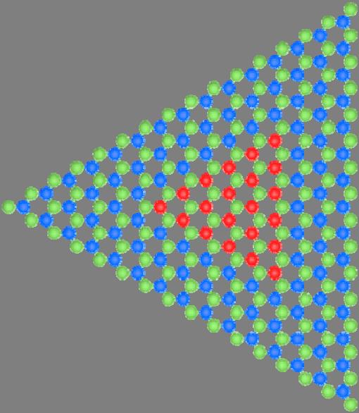
3 Example of device fab Dry transfer technique - Zomer P et al. Appl Phys Lett 105, (2014) Platinum Few layer graphene (FLG) top gate WTe 2 Hexagonal boron nitride - hbn FLG bottom gate 2 5 nm nm ~5 nm nm 2 5 nm SiO nm p++ Si substrate 0.5 mm In the glove box, <0.5 ppm O 2 and H 2 O Exfoliate WTe 2 Pick up on hbn Put down on contacts
 1.0 0.5 0.")


4 Nanotube nanoguitar the most sensitive mass balance Current (a.u.) f res Frequency (MHz) mass unit length adsorbed molecules per C atom 1 f 0 77 K Precision 1 atom, << 1 electron f (MHz) Kr gas pressure Adsorption can also be detected via the conductance


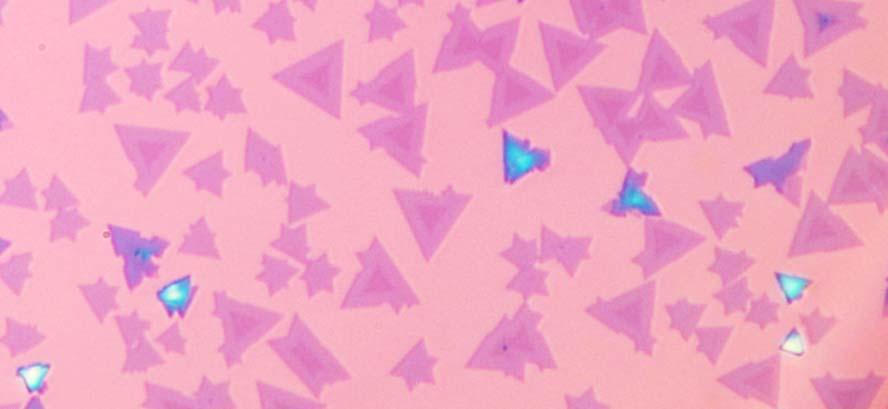
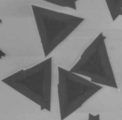
5 Conductance isotherms : studying 2D phase transitions 1 to 2 μm BN After low V anneal After high V anneal Cross section µm µm 0.2 µm AA AB

6 2D semiconductor heterojunctions a WSe 2 Optical SEM Mo W MoSe 2 Photoluminescence TEM 1D edge as substrate WSe 2 lateral heteroepitaxy MoSe 2 Monolayer MoSe 2 formation WSe 2 Mo W Se (x2) WSe 2 /MoSe 2 lateral heterostructure
 k 0 0.4-0.4 (Å -1 ) k 0 0.4-0.4 (Å -1 ) k 0 0.4-0.4 (Å -1 ) k 0 0.4-0.4 (Å -1 ) k 0 0.4 (Å -1 ) -0.")
7 Directly measuring electronic bands Angle resolved photoemission spectroscopy, k Binding Energy, E binding (ev) Vg= -5V Vg= -4V Vg= -3V Vg= -2V Vg= -1V Vg= 0V Vg= +1V Vg= +2V Vg= +3V Vg= +4V Vg=+5V -0.4 k (Å -1 ) k (Å -1 ) k (Å -1 ) k (Å -1 ) k (Å -1 ) k (Å -1 ) -0.4 k (Å -1 ) k (Å -1 ) k (Å -1 ) k (Å -1 ) k (Å -1 ) k (Å -1 ) k (Å -1 ) k (Å -1 ) k (Å -1 ) k (Å -1 ) k (Å -1 ) k (Å -1 ) k (Å -1 ) k (Å -1 ) k (Å -1 ) k (Å -1 )


8 2D magnetism in monolayers CrI 3 15K monolayer bulk 61K Intralayer ferromagnetic Interlayer antiferromagnetic T Kerr rotation bilayer trilayer See Huang et al, Nature (2017) Electric field/strain tunable?


 0.1 0.")
9 2D monolayer semiconductors MoS 2, WSe 2 Electrons are massive Dirac particles with added valley pseudospin Ambipolar monolayer WSe 2 transistor 1 V bg = -4 V V bg = 4 V V sd = 10 mv AC G ( S) V cg (V)


10 3D WTe 2 a van der Waals layered topological semimetal Orthorhombic T d structure W form chains Theory: Type II Weyl points Soluyanov et al. Nature 527, 495 (2015) Huge nonsaturating magnetoresistance at low T Ali, Ong et al, Nature 514, 205 (2014) Monolayer is quantum spin Hall candidate Qian, Junwei Liu, Fu, Li (Science, 2014) 0.53 K


 Majorana mode")
11 The quantum spin Hall (QSH) effect A 2D insulator is topologically nontrivial if invariant 1 Kane & Mele; Kane & Fu, PRL Time-reversal invariant points Λ occupied bands Parity Λ 1implies band inversion 1 Bulk States Edge States If 1there exists at least one gapless mode on the edge +k and k not mixed by time symmetric perturbations possible / quantization Momentum along edge Mode is helical (spin locked to k) quantum spin Hall effect First evidence for QSH reported in HgCdTe (Konig et al, Science 2007) Majorana mode Science News

 1 0 1 600 T (K) 2 40 600 G ( S) 400 200 0 2 0")

12 Few layer WTe 2 devices The first 2D semimetal to be studied Z. Fei et al, Nature Physics (10 April 2017) ~ 300 n p (10 13 cm 2 ) T (K) G ( S) V g (V) e 2 /h T (K) V g (V) e 2 /h V g (V) T (K)


13 Differentiating edge and bulk conduction WTe 2 5 m optical image K AFM image I/V ( S) edge conduction only bulk conduction V g (V)


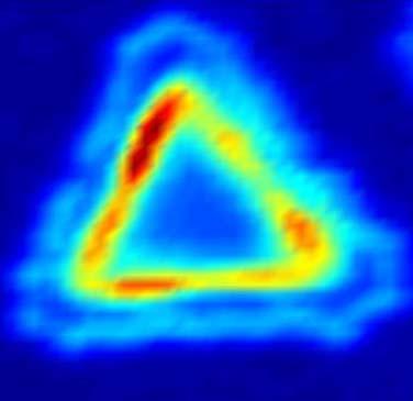
14 Seeing the edge scanning microwave impedance microscopy Measurements by Yongtao Cui, Stanford and UC Riverside Technique: Rev Sci Instr 87, (2016) Brighter = higher conductivity conducting edge Bilayer region 9 GHz 300 mk 0T 12T
15 B field suppresses edge conduction characteristic of QSH G ( S) B B 1.6 K B (T) 120 Conductance ( S) difference =14 T 10 K Gate voltage (V)


16 Weird and wonderful properties of edge conduction T = 1.6 K, L = 150 nm 0 T 1 T 3 T / 5 T 10 T 15 T Bias, Gate voltage,
 Excitonic gap superconducting gap")
17 Phase diagram of monolayer WTe 2 (under construction) 100 strange semimetal Temperature (K) 10 1 metal 0.1 Correlated 2D topological insulator 2D superconductor n p (10 13 cm 2 ) Excitonic gap superconducting gap Quantum phase transition
18 Unpublished data deleted CONCLUSION 2D physics in the lab is going places!
Edge conduction in monolayer WTe 2
 Edge conduction in monolayer WTe 2 Zaiyao Fei 1, Tauno Palomaki 1, Sanfeng Wu 1, Wenjin Zhao 1, Xinghan Cai 1, Bosong Sun 1, Paul Nguyen 1, Joseph Finney 1, Xiaodong Xu 1,2*, and David H. Cobden 1* 1 Department
Coulomb Drag in Graphene
 Graphene 2017 Coulomb Drag in Graphene -Toward Exciton Condensation Philip Kim Department of Physics, Harvard University Coulomb Drag Drag Resistance: R D = V 2 / I 1 Onsager Reciprocity V 2 (B)/ I 1 =
Monolayer Semiconductors
 Monolayer Semiconductors Gilbert Arias California State University San Bernardino University of Washington INT REU, 2013 Advisor: Xiaodong Xu (Dated: August 24, 2013) Abstract Silicon may be unable to
Topology and Correlations in Monolayer Crystals. Sanfeng Wu Department of Physics, MIT UCAS
 Topology and Correlations in Monolayer Crystals Sanfeng Wu Department of Physics, MIT 12/25/2017 @ UCAS Topology and Correlations Quantum Hall Effects Experimental milestones in 1980s: Klaus von Klitzing;
2D MBE Activities in Sheffield. I. Farrer, J. Heffernan Electronic and Electrical Engineering The University of Sheffield
 2D MBE Activities in Sheffield I. Farrer, J. Heffernan Electronic and Electrical Engineering The University of Sheffield Outline Motivation Van der Waals crystals The Transition Metal Di-Chalcogenides
SUPPLEMENTARY INFORMATION
 Lateral heterojunctions within monolayer MoSe 2 -WSe 2 semiconductors Chunming Huang 1,#,*, Sanfeng Wu 1,#,*, Ana M. Sanchez 2,#,*, Jonathan J. P. Peters 2, Richard Beanland 2, Jason S. Ross 3, Pasqual
Solid Surfaces, Interfaces and Thin Films
 Hans Lüth Solid Surfaces, Interfaces and Thin Films Fifth Edition With 427 Figures.2e Springer Contents 1 Surface and Interface Physics: Its Definition and Importance... 1 Panel I: Ultrahigh Vacuum (UHV)
Supplemental Materials for. Interlayer Exciton Optoelectronics in a 2D Heterostructure p-n Junction
 Supplemental Materials for Interlayer Exciton Optoelectronics in a 2D Heterostructure p-n Junction Jason S. Ross 1, Pasqual Rivera 2, John Schaibley 2, Eric Lee-Wong 2, Hongyi Yu 3, Takashi Taniguchi 4,
InAs/GaSb A New 2D Topological Insulator
 InAs/GaSb A New 2D Topological Insulator 1. Old Material for New Physics 2. Quantized Edge Modes 3. Adreev Reflection 4. Summary Rui-Rui Du Rice University Superconductor Hybrids Villard de Lans, France
Emergent Frontiers in Quantum Materials:
 Emergent Frontiers in Quantum Materials: High Temperature superconductivity and Topological Phases Jiun-Haw Chu University of Washington The nature of the problem in Condensed Matter Physics Consider a
Topological 1T -phases patterned onto few-layer semiconducting-phase MoS2 by laser beam irradiation
 Topological 1T -phases patterned onto few-layer semiconducting-phase MoS2 by laser beam irradiation H. Mine 1, A. Kobayashi 1, T. Nakamura 2, T. Inoue 3, J. J. Palacios 4, E. Z. Marin 4, S. Maruyama 3,
Topological Insulators
 Topological Insulators Aira Furusai (Condensed Matter Theory Lab.) = topological insulators (3d and 2d) Outline Introduction: band theory Example of topological insulators: integer quantum Hall effect
Dirac fermions in Graphite:
 Igor Lukyanchuk Amiens University, France, Yakov Kopelevich University of Campinas, Brazil Dirac fermions in Graphite: I. Lukyanchuk, Y. Kopelevich et al. - Phys. Rev. Lett. 93, 166402 (2004) - Phys. Rev.
InAs/GaSb A New Quantum Spin Hall Insulator
 InAs/GaSb A New Quantum Spin Hall Insulator Rui-Rui Du Rice University 1. Old Material for New Physics 2. Quantized Edge Modes 3. Andreev Reflection 4. Summary KITP Workshop on Topological Insulator/Superconductor
2D Materials with Strong Spin-orbit Coupling: Topological and Electronic Transport Properties
 2D Materials with Strong Spin-orbit Coupling: Topological and Electronic Transport Properties Artem Pulkin California Institute of Technology (Caltech), Pasadena, CA 91125, US Institute of Physics, Ecole
Impact of disorder and topology in two dimensional systems at low carrier densities
 Impact of disorder and topology in two dimensional systems at low carrier densities A Thesis Submitted For the Degree of Doctor of Philosophy in the Faculty of Science by Mohammed Ali Aamir Department
Graphite, graphene and relativistic electrons
 Graphite, graphene and relativistic electrons Introduction Physics of E. graphene Y. Andrei Experiments Rutgers University Transport electric field effect Quantum Hall Effect chiral fermions STM Dirac
Transport through Andreev Bound States in a Superconductor-Quantum Dot-Graphene System
 Transport through Andreev Bound States in a Superconductor-Quantum Dot-Graphene System Nadya Mason Travis Dirk, Yung-Fu Chen, Cesar Chialvo Taylor Hughes, Siddhartha Lal, Bruno Uchoa Paul Goldbart University
Edge conduction in monolayer WTe 2
 In the format provided by the authors and unedited. DOI: 1.138/NPHYS491 Edge conduction in monolayer WTe 2 Contents SI-1. Characterizations of monolayer WTe2 devices SI-2. Magnetoresistance and temperature
From Graphene to Silicene: Topological Phase Diagram and Transition
 From Graphene to Silicene: Topological Phase Diagram and Transition EQPCM Symposium Motohiko Ezawa Department of Applied Physics University of Tokyo 1 Outline Silicene is a graphene-like silicon structure
Black phosphorus: A new bandgap tuning knob
 Black phosphorus: A new bandgap tuning knob Rafael Roldán and Andres Castellanos-Gomez Modern electronics rely on devices whose functionality can be adjusted by the end-user with an external knob. A new
Topological Insulators
 Topological Insulators A new state of matter with three dimensional topological electronic order L. Andrew Wray Lawrence Berkeley National Lab Princeton University Surface States (Topological Order in
Fermi polaron-polaritons in MoSe 2
 Fermi polaron-polaritons in MoSe 2 Meinrad Sidler, Patrick Back, Ovidiu Cotlet, Ajit Srivastava, Thomas Fink, Martin Kroner, Eugene Demler, Atac Imamoglu Quantum impurity problem Nonperturbative interaction
Center for Integrated Nanostructure Physics (CINAP)
") Center for Integrated Nanostructure Physics (CINAP) - Institute for Basic Science (IBS) was launched in 2012 by the Korean government to promote basic science in Korea - Our Center was established in 2012
Center for Integrated Nanostructure Physics (CINAP) - Institute for Basic Science (IBS) was launched in 2012 by the Korean government to promote basic science in Korea - Our Center was established in 2012
Chun Ning Lau (Jeanie) Quantum Transport! in! 2D Atomic Membranes!
 Quantum Transport! in! 2D Atomic Membranes!") Chun Ning Lau (Jeanie) Quantum Transport! in! 2D Atomic Membranes! 2D Materials and Heterostructures! hbn MoS 2 WSe 2 Fluorographene Geim, Nature 2013. Conductors, e.g. graphene, few-layer graphene Semiconductors,
Chun Ning Lau (Jeanie) Quantum Transport! in! 2D Atomic Membranes! 2D Materials and Heterostructures! hbn MoS 2 WSe 2 Fluorographene Geim, Nature 2013. Conductors, e.g. graphene, few-layer graphene Semiconductors,
Supplementary Figure 1 Interlayer exciton PL peak position and heterostructure twisting angle. a, Photoluminescence from the interlayer exciton for
 Supplementary Figure 1 Interlayer exciton PL peak position and heterostructure twisting angle. a, Photoluminescence from the interlayer exciton for six WSe 2 -MoSe 2 heterostructures under cw laser excitation
Time - domain THz spectroscopy on the topological insulator Bi2Se3 (and its superconducting bilayers)
") Time - domain THz spectroscopy on the topological insulator Bi2Se3 (and its superconducting bilayers) N. Peter Armitage The Institute of Quantum Matter The Johns Hopkins University Acknowledgements Liang
Time - domain THz spectroscopy on the topological insulator Bi2Se3 (and its superconducting bilayers) N. Peter Armitage The Institute of Quantum Matter The Johns Hopkins University Acknowledgements Liang
Adsorption and Phase Properties of Inert Gases on Suspended Carbon Nanotube Resonators
 Adsorption and Phase Properties of Inert Gases on Suspended Carbon Nanotube Resonators Ricky Roy University of Puget Sound Abstract Carbon nanotubes offer a new regime for adsorption experiments in the
Visualizing Electronic Structures of Quantum Materials By Angle Resolved Photoemission Spectroscopy (ARPES)
") Visualizing Electronic Structures of Quantum Materials By Angle Resolved Photoemission Spectroscopy (ARPES) PART A: ARPES & Application Yulin Chen Oxford University / Tsinghua University www.arpes.org.uk
Visualizing Electronic Structures of Quantum Materials By Angle Resolved Photoemission Spectroscopy (ARPES) PART A: ARPES & Application Yulin Chen Oxford University / Tsinghua University www.arpes.org.uk
Supplementary Figure 1: MoS2 crystals on WSe2-EG and EG and WSe2 crystals on MoSe2-EG and EG.
 Supplementary Figure 1: MoS2 crystals on WSe2-EG and EG and WSe2 crystals on MoSe2-EG and EG. (a) The MoS2 crystals cover both of EG and WSe2/EG after the CVD growth (Scar bar: 400 nm) (b) shows TEM profiles
Magneto-transport Study of 3D Topological Insulator Bi2Te3 And GaAs/AlGaAs 2D Electron System
 Georgia State University ScholarWorks @ Georgia State University Physics and Astronomy Dissertations Department of Physics and Astronomy 8-8-2017 Magneto-transport Study of 3D Topological Insulator Bi2Te3
Bloch, Landau, and Dirac: Hofstadter s Butterfly in Graphene. Philip Kim. Physics Department, Columbia University
 Bloch, Landau, and Dirac: Hofstadter s Butterfly in Graphene Philip Kim Physics Department, Columbia University Acknowledgment Prof. Cory Dean (now at CUNY) Lei Wang Patrick Maher Fereshte Ghahari Carlos
Dirac matter: Magneto-optical studies
 Dirac matter: Magneto-optical studies Marek Potemski Laboratoire National des Champs Magnétiques Intenses Grenoble High Magnetic Field Laboratory CNRS/UGA/UPS/INSA/EMFL MOMB nd International Conference
Supplementary Figure 1 Experimental setup for crystal growth. Schematic drawing of the experimental setup for C 8 -BTBT crystal growth.
 Supplementary Figure 1 Experimental setup for crystal growth. Schematic drawing of the experimental setup for C 8 -BTBT crystal growth. Supplementary Figure 2 AFM study of the C 8 -BTBT crystal growth
Bridging the Gap: Black Phosphorus for Electronics and Photonics
 IBM Thomas J. Watson Research Center Bridging the Gap: Black Phosphorus for Electronics and Photonics Fengnian Xia Department of Electrical Engineering Yale University, New Haven CT 06511 Email: fengnian.ia@yale.edu
2D Materials for Gas Sensing
 2D Materials for Gas Sensing S. Guo, A. Rani, and M.E. Zaghloul Department of Electrical and Computer Engineering The George Washington University, Washington DC 20052 Outline Background Structures of
Supplementary Information for
 Supplementary Information for Highly Stable, Dual-Gated MoS 2 Transistors Encapsulated by Hexagonal Boron Nitride with Gate-Controllable Contact Resistance and Threshold Voltage Gwan-Hyoung Lee, Xu Cui,
Topological insulator gap in graphene with heavy adatoms
 Topological insulator gap in graphene with heavy adatoms ES2013, College of William and Mary Ruqian Wu Department of Physics and Astronomy, University of California, Irvine, California 92697 Supported
Observation of topological surface state quantum Hall effect in an intrinsic three-dimensional topological insulator
 Observation of topological surface state quantum Hall effect in an intrinsic three-dimensional topological insulator Authors: Yang Xu 1,2, Ireneusz Miotkowski 1, Chang Liu 3,4, Jifa Tian 1,2, Hyoungdo
Hrudya Nair. COBDEN RESEARCH GROUP Nanodevice Physics Lab CAPACITOR BRIDGE
 Hrudya Nair COBDEN RESEARCH GROUP Nanodevice Physics Lab CAPACITOR BRIDGE Overview: In this lab students will learn to measure the capacitance of an unknown capacitor by building a capacitor bridge circuit
Spin Hall and quantum spin Hall effects. Shuichi Murakami Department of Physics, Tokyo Institute of Technology PRESTO, JST
 YKIS2007 (Kyoto) Nov.16, 2007 Spin Hall and quantum spin Hall effects Shuichi Murakami Department of Physics, Tokyo Institute of Technology PRESTO, JST Introduction Spin Hall effect spin Hall effect in
A BIT OF MATERIALS SCIENCE THEN PHYSICS
 GRAPHENE AND OTHER D ATOMIC CRYSTALS Andre Geim with many thanks to K. Novoselov, S. Morozov, D. Jiang, F. Schedin, I. Grigorieva, J. Meyer, M. Katsnelson A BIT OF MATERIALS SCIENCE THEN PHYSICS CARBON
Supplementary Figure S1. AFM images of GraNRs grown with standard growth process. Each of these pictures show GraNRs prepared independently,
 Supplementary Figure S1. AFM images of GraNRs grown with standard growth process. Each of these pictures show GraNRs prepared independently, suggesting that the results is reproducible. Supplementary Figure
Observation of the Quantum Spin Hall Effect up to 100 Kelvin in a Monolayer Crystal
 Observation of the Quantum Spin Hall Effect up to 100 Kelvin in a Monolayer Crystal Authors: Sanfeng Wu 1, #, *, Valla Fatemi 1, #, *, Quinn D. Gibson 2, Kenji Watanabe 3, Takashi Taniguchi 3, Robert J.
3D Weyl metallic states realized in the Bi 1-x Sb x alloy and BiTeI. Heon-Jung Kim Department of Physics, Daegu University, Korea
 3D Weyl metallic states realized in the Bi 1-x Sb x alloy and BiTeI Heon-Jung Kim Department of Physics, Daegu University, Korea Content 3D Dirac metals Search for 3D generalization of graphene Bi 1-x
Supporting information. Gate-optimized thermoelectric power factor in ultrathin WSe2 single crystals
 Supporting information Gate-optimized thermoelectric power factor in ultrathin WSe2 single crystals Masaro Yoshida 1, Takahiko Iizuka 1, Yu Saito 1, Masaru Onga 1, Ryuji Suzuki 1, Yijin Zhang 1, Yoshihiro
Introductory lecture on topological insulators. Reza Asgari
 Introductory lecture on topological insulators Reza Asgari Workshop on graphene and topological insulators, IPM. 19-20 Oct. 2011 Outlines -Introduction New phases of materials, Insulators -Theory quantum
Spatially resolving density-dependent screening around a single charged atom in graphene
 Supplementary Information for Spatially resolving density-dependent screening around a single charged atom in graphene Dillon Wong, Fabiano Corsetti, Yang Wang, Victor W. Brar, Hsin-Zon Tsai, Qiong Wu,
Spin-Conserving Resonant Tunneling in Twist- Supporting Information
 Spin-Conserving Resonant Tunneling in Twist- Controlled WSe2-hBN-WSe2 Heterostructures Supporting Information Kyounghwan Kim, 1 Nitin Prasad, 1 Hema C. P. Movva, 1 G. William Burg, 1 Yimeng Wang, 1 Stefano
Graphene and Carbon Nanotubes
 Graphene and Carbon Nanotubes 1 atom thick films of graphite atomic chicken wire Novoselov et al - Science 306, 666 (004) 100μm Geim s group at Manchester Novoselov et al - Nature 438, 197 (005) Kim-Stormer
Massive Dirac Fermion on the Surface of a magnetically doped Topological Insulator
 SLAC-PUB-14357 Massive Dirac Fermion on the Surface of a magnetically doped Topological Insulator Y. L. Chen 1,2,3, J.-H. Chu 1,2, J. G. Analytis 1,2, Z. K. Liu 1,2, K. Igarashi 4, H.-H. Kuo 1,2, X. L.
Supplementary Materials for
 advances.sciencemag.org/cgi/content/full/3/2/e1601832/dc1 Supplementary Materials for Determination of band offsets, hybridization, and exciton binding in 2D semiconductor heterostructures Neil R. Wilson,
Supporting Information Available:
 Supporting Information Available: Photoresponsive and Gas Sensing Field-Effect Transistors based on Multilayer WS 2 Nanoflakes Nengjie Huo 1, Shengxue Yang 1, Zhongming Wei 2, Shu-Shen Li 1, Jian-Bai Xia
From nanophysics research labs to cell phones. Dr. András Halbritter Department of Physics associate professor
 From nanophysics research labs to cell phones Dr. András Halbritter Department of Physics associate professor Curriculum Vitae Birth: 1976. High-school graduation: 1994. Master degree: 1999. PhD: 2003.
SUPPLEMENTARY INFORMATION
 doi:10.1038/nature13734 1. Gate dependence of the negatively charged trion in WS 2 monolayer. We test the trion with both transport and optical measurements. The trion in our system is negatively charged,
Scanning Tunneling Microscopy Studies of Topological Insulators Grown by Molecular Beam Epitaxy
 EPJ Web of Conferences 23, 00020 ( 2012) DOI: 10.1051/ epjconf/ 20122300020 C Owned by the authors, published by EDP Sciences, 2012 Scanning Tunneling Microscopy Studies of Topological Insulators Grown
Overview. Carbon in all its forms. Background & Discovery Fabrication. Important properties. Summary & References. Overview of current research
 Graphene Prepared for Solid State Physics II Pr Dagotto Spring 2009 Laurene Tetard 03/23/09 Overview Carbon in all its forms Background & Discovery Fabrication Important properties Overview of current
Seminars in Nanosystems - I
 Seminars in Nanosystems - I Winter Semester 2011/2012 Dr. Emanuela Margapoti Emanuela.Margapoti@wsi.tum.de Dr. Gregor Koblmüller Gregor.Koblmueller@wsi.tum.de Seminar Room at ZNN 1 floor Topics of the
Outline. Introduction: graphene. Adsorption on graphene: - Chemisorption - Physisorption. Summary
 Outline Introduction: graphene Adsorption on graphene: - Chemisorption - Physisorption Summary 1 Electronic band structure: Electronic properties K Γ M v F = 10 6 ms -1 = c/300 massless Dirac particles!
Spin-orbit proximity effects in graphene on TMDCs. Jaroslav Fabian
 Hvar, 4.10.2017 Spin-orbit proximity effects in graphene on TMDCs Jaroslav Fabian Institute for Theoretical Physics University of Regensburg SFB1277 GRK TI SPP 1666 SFB689 GRK1570 SPP 1538 Arbeitsgruppe
SUPPLEMENTARY INFORMATION
 SUPPLEMENTARY INFORMATION SUPPLEMENTARY INFORMATION Trilayer graphene is a semimetal with a gate-tuneable band overlap M. F. Craciun, S. Russo, M. Yamamoto, J. B. Oostinga, A. F. Morpurgo and S. Tarucha
Supporting Information. by Hexagonal Boron Nitride
 Supporting Information High Velocity Saturation in Graphene Encapsulated by Hexagonal Boron Nitride Megan A. Yamoah 1,2,, Wenmin Yang 1,3, Eric Pop 4,5,6, David Goldhaber-Gordon 1 * 1 Department of Physics,
Topological insulators
 http://www.physik.uni-regensburg.de/forschung/fabian Topological insulators Jaroslav Fabian Institute for Theoretical Physics University of Regensburg Stara Lesna, 21.8.212 DFG SFB 689 what are topological
Center for Spintronic Materials, Interfaces, and Novel Architectures. Voltage Controlled Antiferromagnetics and Future Spin Memory
 Center for Spintronic Materials, Interfaces, and Novel Architectures Voltage Controlled Antiferromagnetics and Future Spin Memory Maxim Tsoi The University of Texas at Austin Acknowledgments: H. Seinige,
Terahertz sensing and imaging based on carbon nanotubes:
 Terahertz sensing and imaging based on carbon nanotubes: Frequency-selective detection and near-field imaging Yukio Kawano RIKEN, JST PRESTO ykawano@riken.jp http://www.riken.jp/lab-www/adv_device/kawano/index.html
Optical properties of single-layer, double-layer, and bulk MoS2
 Optical properties of single-layer, double-layer, and bulk MoS Alejandro Molina-Sánchez, Ludger Wirtz, Davide Sangalli, Andrea Marini, Kerstin Hummer Single-layer semiconductors From graphene to a new
Supplementary Figure 2 Photoluminescence in 1L- (black line) and 7L-MoS 2 (red line) of the Figure 1B with illuminated wavelength of 543 nm.
 and 7L-MoS 2 (red line) of the Figure 1B with illuminated wavelength of 543 nm.") PL (normalized) Intensity (arb. u.) 1 1 8 7L-MoS 1L-MoS 6 4 37 38 39 4 41 4 Raman shift (cm -1 ) Supplementary Figure 1 Raman spectra of the Figure 1B at the 1L-MoS area (black line) and 7L-MoS area (red
PL (normalized) Intensity (arb. u.) 1 1 8 7L-MoS 1L-MoS 6 4 37 38 39 4 41 4 Raman shift (cm -1 ) Supplementary Figure 1 Raman spectra of the Figure 1B at the 1L-MoS area (black line) and 7L-MoS area (red
Ferromagnetism and Anomalous Hall Effect in Graphene
 Ferromagnetism and Anomalous Hall Effect in Graphene Jing Shi Department of Physics & Astronomy, University of California, Riverside Graphene/YIG Introduction Outline Proximity induced ferromagnetism Quantized
Abstract. Introduction
 Two Dimensional Maps of Photoluminescence and Second Harmonic Generation Tara Boland University of North Dakota University of Washington INT REU, 2014 Advisor: Xiaodong Xu (Dated: August 31, 2014) Abstract
arxiv: v1 [cond-mat.mes-hall] 29 Jul 2010
![arxiv: v1 [cond-mat.mes-hall] 29 Jul 2010](/thumbs/94/121300146.jpg "arxiv: v1 [cond-mat.mes-hall] 29 Jul 2010") Discovery of several large families of Topological Insulator classes with backscattering-suppressed spin-polarized single-dirac-cone on the surface arxiv:1007.5111v1 [cond-mat.mes-hall] 29 Jul 2010 Su-Yang
Discovery of several large families of Topological Insulator classes with backscattering-suppressed spin-polarized single-dirac-cone on the surface arxiv:1007.5111v1 [cond-mat.mes-hall] 29 Jul 2010 Su-Yang
Supporting Information. Tuning Interlayer Coupling in Large-area Heterostructures with CVD-grown MoS 2 and WS 2 monolayers
 Supporting Information Tuning Interlayer Coupling in Large-area Heterostructures with CVD-grown MoS 2 and WS 2 monolayers Sefaattin Tongay 1,, Wen Fan 1,2,, Jun Kang 3, Joonsuk Park 4,Unsal Koldemir 4,Joonki
Electronics with 2D Crystals: Scaling extender, or harbinger of new functions?
 Electronics with 2D Crystals: Scaling extender, or harbinger of new functions? 1 st Workshop on Data Abundant Systems Technology Stanford, April 2014 Debdeep Jena (djena@nd.edu) Electrical Engineering,
Quantum Hall effect and Landau level crossing of Dirac fermions in trilayer graphene Supplementary Information
 Quantum Hall effect and Landau level crossing of Dirac fermions in trilayer graphene Supplementary Information Thiti Taychatanapat, Kenji Watanabe, Takashi Taniguchi, Pablo Jarillo-Herrero Department of
SUPPLEMENTARY INFORMATION. Observation of tunable electrical bandgap in large-area twisted bilayer graphene synthesized by chemical vapor deposition
 SUPPLEMENTARY INFORMATION Observation of tunable electrical bandgap in large-area twisted bilayer graphene synthesized by chemical vapor deposition Jing-Bo Liu 1 *, Ping-Jian Li 1 *, Yuan-Fu Chen 1, Ze-Gao
Self-Assembly of Two-Dimensional Organic Networks Containing Heavy Metals (Pb, Bi) and Preparation of Spin-Polarized Scanning Tunneling Microscope
 and Preparation of Spin-Polarized Scanning Tunneling Microscope") MPhil Thesis Defense Self-Assembly of Two-Dimensional Organic Networks Containing Heavy Metals (Pb, Bi) and Preparation of Spin-Polarized Scanning Tunneling Microscope Presented by CHEN Cheng 12 th Aug.
MPhil Thesis Defense Self-Assembly of Two-Dimensional Organic Networks Containing Heavy Metals (Pb, Bi) and Preparation of Spin-Polarized Scanning Tunneling Microscope Presented by CHEN Cheng 12 th Aug.
Topological Defects in the Topological Insulator
 Topological Defects in the Topological Insulator Ashvin Vishwanath UC Berkeley arxiv:0810.5121 YING RAN Frank YI ZHANG Quantum Hall States Exotic Band Topology Topological band Insulators (quantum spin
SUPPLEMENTARY INFORMATION
 SUPPLEMENTARY INFORMATION Facile Synthesis of High Quality Graphene Nanoribbons Liying Jiao, Xinran Wang, Georgi Diankov, Hailiang Wang & Hongjie Dai* Supplementary Information 1. Photograph of graphene
QS School Summary
 2018 NSF/DOE/AFOSR Quantum Science Summer School June 22, 2018 QS 3 2018 School Summary Kyle Shen (Cornell) Some Thank yous! A Big Thanks to Caroline Brockner!!! Also to our fantastic speakers! Kavli Institute
TRANSVERSE SPIN TRANSPORT IN GRAPHENE
 International Journal of Modern Physics B Vol. 23, Nos. 12 & 13 (2009) 2641 2646 World Scientific Publishing Company TRANSVERSE SPIN TRANSPORT IN GRAPHENE TARIQ M. G. MOHIUDDIN, A. A. ZHUKOV, D. C. ELIAS,
New Quantum Transport Results in Type-II InAs/GaSb Quantum Wells
 New Quantum Transport Results in Type-II InAs/GaSb Quantum Wells Wei Pan Sandia National Laboratories Sandia National Laboratories is a multi-program laboratory managed and operated by Sandia Corporation,
Topological Defects inside a Topological Band Insulator
 Topological Defects inside a Topological Band Insulator Ashvin Vishwanath UC Berkeley Refs: Ran, Zhang A.V., Nature Physics 5, 289 (2009). Hosur, Ryu, AV arxiv: 0908.2691 Part 1: Outline A toy model of
Tutorial: Berry phase and Berry curvature in solids
 Tutorial: Berry phase and Berry curvature in solids Justin Song Division of Physics, Nanyang Technological University (Singapore) & Institute of High Performance Computing (Singapore) Funding: (Singapore)
Topological Photonics with Heavy-Photon Bands
 Topological Photonics with Heavy-Photon Bands Vassilios Yannopapas Dept. of Physics, National Technical University of Athens (NTUA) Quantum simulations and many-body physics with light, 4-11/6/2016, Hania,
Let There Be Topological Superconductors
 Let There Be Topological Superconductors K K d Γ ~q c µ arxiv:1606.00857 arxiv:1603.02692 Eun-Ah Kim (Cornell) Boulder 7.21-22.2016 Q. Topological Superconductor material? Bulk 1D proximity 2D proximity?
Effects of Interactions in Suspended Graphene
 Effects of Interactions in Suspended Graphene Ben Feldman, Andrei Levin, Amir Yacoby, Harvard University Broken and unbroken symmetries in the lowest LL: spin and valley symmetries. FQHE Discussions with
Supplementary Information
 Supplementary Information Supplementary Figure S1: Ab initio band structures in presence of spin-orbit coupling. Energy bands for (a) MoS 2, (b) MoSe 2, (c) WS 2, and (d) WSe 2 bilayers. It is worth noting
Supplementary Figure 1. Selected area electron diffraction (SAED) of bilayer graphene and tblg. (a) AB
 of bilayer graphene and tblg. (a) AB") Supplementary Figure 1. Selected area electron diffraction (SAED) of bilayer graphene and tblg. (a) AB stacked bilayer graphene (b), (c), (d), (e), and (f) are twisted bilayer graphene with twist angle
Supplementary Figure 1. Selected area electron diffraction (SAED) of bilayer graphene and tblg. (a) AB stacked bilayer graphene (b), (c), (d), (e), and (f) are twisted bilayer graphene with twist angle
Tunable Band Gap of Silicene on Monolayer Gallium Phosphide Substrate
 2017 International Conference on Energy Development and Environmental Protection (EDEP 2017) ISBN: 978-1-60595-482-0 Tunable Band Gap of Silicene on Monolayer Gallium Phosphide Substrate Miao-Juan REN
Topological Surface States Protected From Backscattering by Chiral Spin Texture
 1 Topological Surface States Protected From Backscattering by Chiral Spin Texture Pedram Roushan 1, Jungpil Seo 1, Colin V. Parker 1, Y. S. Hor 2, D. Hsieh 1, Dong Qian 1, Anthony Richardella 1, M. Z.
Supporting Information for. Interfacial Electronic States and Self-Formed p-n Junctions in
 Electronic Supplementary Material (ESI) for Journal of Materials Chemistry C. This journal is The Royal Society of Chemistry 2018 Supporting Information for Interfacial Electronic States and Self-Formed
Topological insulators and the quantum anomalous Hall state. David Vanderbilt Rutgers University
 Topological insulators and the quantum anomalous Hall state David Vanderbilt Rutgers University Outline Berry curvature and topology 2D quantum anomalous Hall (QAH) insulator TR-invariant insulators (Z
Supplementary Information
 Supplementary Information Supplementary Figure 1 AFM and Raman characterization of WS 2 crystals. (a) Optical and AFM images of a representative WS 2 flake. Color scale of the AFM image represents 0-20
Direct imaging of topological edge states at a bilayer graphene domain wall
 Direct imaging of topological edge states at a bilayer graphene domain wall Long-Jing Yin 1, Hua Jiang 2, Jia-Bin Qiao 1, Lin He 1, * 1 Center for Advanced Quantum Studies, Department of Physics, Beijing
Electrical control of the valley Hall effect in bilayer MoS2 transistors
 Electrical control of the valley Hall effect in bilayer MoS2 transistors Jieun Lee, Kin Fai Mak*, and Jie Shan* Department of Physics and Center for 2-Dimensional and Layered Materials, The Pennsylvania
Commensuration and Incommensuration in the van der Waals Heterojunctions. Philip Kim Physics Department Harvard University
 Commensuration and Incommensuration in the van der Waals Heterojunctions Philip Kim Physics Department Harvard University Rise of 2D van der Waals Systems graphene Metal-Chalcogenide Bi 2 Sr 2 CaCu 2 O
Chern insulator and Chern half-metal states in the two-dimensional. spin-gapless semiconductor Mn 2 C 6 S 12
 Supporting Information for Chern insulator and Chern half-metal states in the two-dimensional spin-gapless semiconductor Mn 2 C 6 S 12 Aizhu Wang 1,2, Xiaoming Zhang 1, Yuanping Feng 3 * and Mingwen Zhao
Laurens W. Molenkamp. Physikalisches Institut, EP3 Universität Würzburg
 Laurens W. Molenkamp Physikalisches Institut, EP3 Universität Würzburg Overview - HgTe/CdTe bandstructure, quantum spin Hall effect: 2D TI - Dirac surface states of strained bulk HgTe: 3D TI - Topological
Graphene The Search For Two Dimensions. Christopher Scott Friedline Arizona State University
 Graphene The Search For Two Dimensions Christopher Scott Friedline Arizona State University What Is Graphene? Single atomic layer of graphite arranged in a honeycomb crystal lattice Consists of sp 2 -bonded
Anomalous Metals and Failed Superconductors. With B. Spivak and A. Kapitulnik (also P. Oreto)
") Anomalous Metals and Failed Superconductors With B. Spivak and A. Kapitulnik (also P. Oreto) Tallahassee 2018 Pillars the Theory of Quantum Mater From B Spivak Α proof of the Fermi liquid theory is based
Anomalous Metals and Failed Superconductors With B. Spivak and A. Kapitulnik (also P. Oreto) Tallahassee 2018 Pillars the Theory of Quantum Mater From B Spivak Α proof of the Fermi liquid theory is based
TEOS characterization of 2D materials from graphene to TMDCs
 Marc Chaigneau Yoshito Okuno, Andrey Krayev, Filippo Fabbri HORIBA Scientific AIST-NT Inc. IMEM-CNR Institute TEOS characterization of 2D materials from graphene to TMDCs 30-03-2017 Graphene2017 2015 2017