Graphene and Carbon Nanotubes
|
|
|
- Kenneth Bennett
- 6 years ago
- Views:
Transcription


 Zhang et al")

1 Graphene and Carbon Nanotubes 1 atom thick films of graphite atomic chicken wire Novoselov et al - Science 306, 666 (004) 100μm Geim s group at Manchester Novoselov et al - Nature 438, 197 (005) Kim-Stormer group at Columbia University Zhang et al - PRL 94, (005) Zhang et al - Nature 438, 01 (005) One atom thick layer of graphite = graphene


 Tight")
2 Scanning Transmission Electron micrograph of GRAPHENE Thanks to Dr Nicolosi (Oxford Materials) Tight binding Calculation: Graphene antibonding
 Non-hybridized (pi) electrons play key role in graphene")
3 Tight binding Calculation: Graphene antibonding Graphene bandstructure N N N N NB, Two C atoms per unit cell (ie 1 electrons, 8 of which are valence) Non-hybridized (pi) electrons play key role in graphene conductivity

4 c Tight Binding Theory 3 a * 0 0 K c c K * = 1 x 10 6 ms -1 * * 1 ck 1 E Typical values of are in the region of 3 ev, β = ~0.1, giving: c / c million k.p.h. Minimum conductance at K (Dirac)-point Conductance minimum as Fermi energy passes through zero density of states Manchester and Columbia groups 0 ne e h ne l mv F X 4 e h k F l Mott criterion: k F l 1


5 A graphene based future Graphene predicted to lead to lots of new physics + New fast transistors, super strength materials, transparent electrodes, chemical sensors... Single walled Carbon nanotubes: Discovered in 1993!


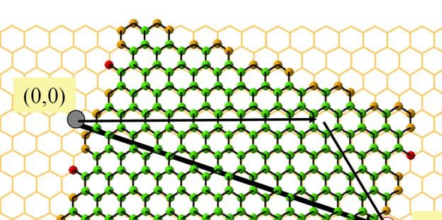
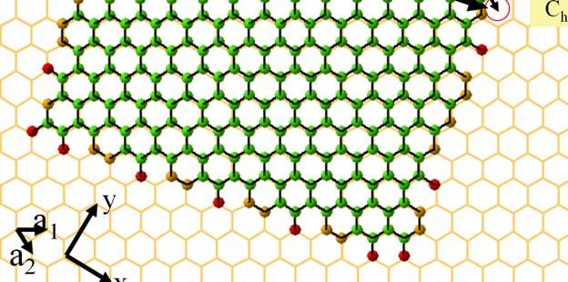
6 Carbon nanotubes: rolled up graphene! (10,10) Armchair Carbon Nanotubes Wrapping (10,5) SWNT (0,0) C h = (10,5) a a 1 y x
 are called zigzag nanotubes (n,n) are called armchair nanotubes Chiral angle (definition) Carbon Nanotubes Cyclic boundary conditions give allowed")
7 Carbon Nanotubes (CNTs) Chiral vector for CNT Tube diameter (5,) CNT translation vector Greatest common devisor of Number of hexagons in nanotube unit cell: 1 st lattice point reached! Chiral vectors are used to label CNTs: (n,0) are called zigzag nanotubes (n,n) are called armchair nanotubes Chiral angle (definition) Carbon Nanotubes Cyclic boundary conditions give allowed k-states for CNT: Where reciprocal lattice vectors for CNT unit cell: Number of CNT translation vectors along full length of tube (circumference recip. lattice vector) (CNT axis recip. lattice vector) If allowed k-state coincides with graphene 1st BZ K point = metallic!
8 Allowed k-states for a (3,1) CNT Extended Brillouin Zone Scheme Zone Folded Scheme Tight binding Calculation: Graphene antibonding

 metallic")
9 Tight binding Calculation: Graphene antibonding Carbon Nanotubes (examples) (7,4) (7,6) metallic semiconducting


10 Carbon Nanotube Bandgaps Carbon Nanotubes (examples) Armchair CNT Zigzag CNT Zigzag CNT METAL METAL SEMICONDUCTOR


 Bandstructure NB 1-D")
11 Carbon nanotubes: metallic if n 1 n is a multiple of 3 zigzag 1,0,0 4,0 5,0 7,0 8,0,1 3,1 5,1 6,1 8,1 3, 4, 6, 7, 4,3 5,3 7,3 5,4 6,4 6,5 Metallic armchair Semiconducting 10,011,0 9,1 9, 8,3 8,4 7,5 7,6 11,1 10, 10,3 9,4 9,5 8,6 8,7 CNT (1-D) Bandstructure NB 1-D CNT Brillouin Zone
 semiconducting Photo-Luminescence")

12 CNT (1-D) Density of States (8,8) metallic (8,0) semiconducting Photo-Luminescence Excitation Mapping Scan E excitation energy and measure emission from E11. Luminescence (fluorescence)

13 Low Dimensional Structures and Materials Artificial layered structures - Quantum Wells and Superlattices Electric or Magnetic Fields applied in one direction. Layers may be only a few atoms thick Heterojunctions Energy levels for different semiconductors Energy line up at junction of two (undoped) materials
14 Reduced Dimensionality Quantum Well removes 1 Dimension by quantization Electron is bound in well and can only move in plane -D system - motion in x, y plane Quantum Mechanical Engineering quantum wells give levels (symmetric and antisymmetric combinations) Superlattice generates a (mini)band E 0 k /L
15 Quantum Well - Type I Typical Materials: 1: GaAs : (Al 0.35 Ga 0.65 )As (E g = 1.5 ev) (E g =.0 ev) Energy levels are quantized in z-direction with values E n for both electrons and holes E = E n + k /m* 1-D -D Infinite well - Particle in a box 1-D Motion in z-direction d E m* dz nz na sin L L n = 3 n = E n n m* L k m* n = 1 Typical values L = 10 nm, m e * = 0.07 m e E n = 54 n mev System is Two-Dimensional when: E -E 1 > kt 16 mev 5 mev at 300 K
16 Finite Well even parity odd parity n (z) Acos kz Asin kz z < L/ Bexp[-(z - L/)] Bexp[-(z - L/ z > L/ Bexp[+(z + L/)] -Bexp[+(z + L/)] z < L/ where: n k V0 m * m * 1 assume m 1 =m k + =k 0 =m*v 0 / boundary conditions: wavefunction 1 = probability current A cos (kl/) = B ka sin (kl/) = B m z m z 1 A sin (kl/) = B ka cos (kl/) = -B k tan (kl/) = k cot (kl/) = k sec (kl/) = k 0 k cosec (kl/) = k 0 cos (kl/) = k/k 0 sin (kl/) = k/k 0
17 Graphical solution of finite Quantum Well Well depth determines value of slope k 0-1
18 Optical Properties 3-D Absorption coefficient is proportional to the density of states: ~ 1/ Modified close to the band gap due to excitons -D - Big Changes Multiple Band gaps - Band gap shift - Sharper edge For wide wells the sum of many -D absorptions becomes equivalent to the 3-D absorption shape ( 1/ ) Correspondence principle.
19 GaAs/Al 0.35 Ga 0.65 As Quantum Well absorption Sharp peaks due to excitons peaks doubled due to heavy and light holes Semiconductor lasers Forward biased p-n junction Quantum Well laser Fibre Optic Communications, CD players, laser pointers
 Epitaxy - maintaining crystal structure of the substrate - which is a single crystal Metal")
 3 Ga + AsH 3 GaAs + 3CH 4 Reaction takes place on a heated substrate and growth is also")
20 Molecular Beam Epitaxy (MBE) Ultra High Vacuum evaporation of molecular species of elements (Molecular Beam) Epitaxy - maintaining crystal structure of the substrate - which is a single crystal Metal Organic Vapour Phase Epitaxy (MOVPE) Chemical reaction of elements bonded in volatile organic compounds e.g. (CH 3 ) 3 Ga + AsH 3 GaAs + 3CH 4 Reaction takes place on a heated substrate and growth is also epitaxial
21 Heterojunctions and Modulation Doping New idea for superlattices and heterojunctions: Separate the dopant impurities from the electrons Gated structures Place metallic electrode on surface to apply variable electric field gives a variable potential and surface charge density Basis of MOS transistors as well as controllable -D systems.

22 Negative electrode potential repels electrons underneath leaving only a narrow 1-D channel of conducting electrons Quantized Conductance in 1-D - the Quantum Point Contact For a short 1-D structure there is no scattering - Ballistic transport Calculate the current carried by the electrons by adding up the contributions from all carriers travelling in one direction. For flow in one direction only (k > 0) the density of states is: 1 L m 1 * / 1 / d i.e. half the usual 1-D density of states, but with a factor to account for spin degeneracy.
23 The electrons have velocity v = (/m*) 1/. Therefore the current in the positive direction is: J 0 e v g( ) d e h Apply a voltage V along the 1-D channel to give a difference in chemical potential. This causes a net current to flow: J Tot. J J e h 0 d e h ev 0 d e h V Therefore the conductance is: When there are p 1-D subbands occupied (e.g. if the 1-D wire is wider) each contributes one unit of conductance Total J Tot. V e h e p h B.J. van Wees et al, Phys. Rev. Lett. 60, 848 (1988)
Quantized Electrical Conductance of Carbon nanotubes(cnts)
") Quantized Electrical Conductance of Carbon nanotubes(cnts) By Boxiao Chen PH 464: Applied Optics Instructor: Andres L arosa Abstract One of the main factors that impacts the efficiency of solar cells is
Quantized Electrical Conductance of Carbon nanotubes(cnts) By Boxiao Chen PH 464: Applied Optics Instructor: Andres L arosa Abstract One of the main factors that impacts the efficiency of solar cells is
Calculating Electronic Structure of Different Carbon Nanotubes and its Affect on Band Gap
 Calculating Electronic Structure of Different Carbon Nanotubes and its Affect on Band Gap 1 Rashid Nizam, 2 S. Mahdi A. Rizvi, 3 Ameer Azam 1 Centre of Excellence in Material Science, Applied Physics AMU,
CHAPTER 6 CHIRALITY AND SIZE EFFECT IN SINGLE WALLED CARBON NANOTUBES
 10 CHAPTER 6 CHIRALITY AND SIZE EFFECT IN SINGLE WALLED CARBON NANOTUBES 6.1 PREAMBLE Lot of research work is in progress to investigate the properties of CNTs for possible technological applications.
Lecture 20: Semiconductor Structures Kittel Ch 17, p , extra material in the class notes
 Lecture 20: Semiconductor Structures Kittel Ch 17, p 494-503, 507-511 + extra material in the class notes MOS Structure Layer Structure metal Oxide insulator Semiconductor Semiconductor Large-gap Semiconductor
chiral m = n Armchair m = 0 or n = 0 Zigzag m n Chiral Three major categories of nanotube structures can be identified based on the values of m and n
 zigzag armchair Three major categories of nanotube structures can be identified based on the values of m and n m = n Armchair m = 0 or n = 0 Zigzag m n Chiral Nature 391, 59, (1998) chiral J. Tersoff,
Carbon nanotubes and Graphene
 16 October, 2008 Solid State Physics Seminar Main points 1 History and discovery of Graphene and Carbon nanotubes 2 Tight-binding approximation Dynamics of electrons near the Dirac-points 3 Properties
Physics and technology of nanosize structures
 1 Universidade de Aveiro Departamento de Física Nikolai A. Sobolev, Svetlana P. Kobeleva Physics and technology of nanosize structures 014/015 Национальный исследовательский технологический университет
Heterostructures and sub-bands
 Heterostructures and sub-bands (Read Datta 6.1, 6.2; Davies 4.1-4.5) Quantum Wells In a quantum well, electrons are confined in one of three dimensions to exist within a region of length L z. If the barriers
Electron Interactions and Nanotube Fluorescence Spectroscopy C.L. Kane & E.J. Mele
 Electron Interactions and Nanotube Fluorescence Spectroscopy C.L. Kane & E.J. Mele Large radius theory of optical transitions in semiconducting nanotubes derived from low energy theory of graphene Phys.
ELECTRONIC ENERGY DISPERSION AND STRUCTURAL PROPERTIES ON GRAPHENE AND CARBON NANOTUBES
 ELECTRONIC ENERGY DISPERSION AND STRUCTURAL PROPERTIES ON GRAPHENE AND CARBON NANOTUBES D. RACOLTA, C. ANDRONACHE, D. TODORAN, R. TODORAN Technical University of Cluj Napoca, North University Center of
2 Symmetry. 2.1 Structure of carbon nanotubes
 2 Symmetry Carbon nanotubes are hollow cylinders of graphite sheets. They can be viewed as single molecules, regarding their small size ( nm in diameter and µm length), or as quasi-one dimensional crystals
3-month progress Report
 3-month progress Report Graphene Devices and Circuits Supervisor Dr. P.A Childs Table of Content Abstract... 1 1. Introduction... 1 1.1 Graphene gold rush... 1 1.2 Properties of graphene... 3 1.3 Semiconductor
Refering to Fig. 1 the lattice vectors can be written as: ~a 2 = a 0. We start with the following Ansatz for the wavefunction:
 1 INTRODUCTION 1 Bandstructure of Graphene and Carbon Nanotubes: An Exercise in Condensed Matter Physics developed by Christian Schönenberger, April 1 Introduction This is an example for the application
Lectures Graphene and
 Lectures 15-16 Graphene and carbon nanotubes Graphene is atomically thin crystal of carbon which is stronger than steel but flexible, is transparent for light, and conducts electricity (gapless semiconductor).
Introduction to Nanotechnology Chapter 5 Carbon Nanostructures Lecture 1
 Introduction to Nanotechnology Chapter 5 Carbon Nanostructures Lecture 1 ChiiDong Chen Institute of Physics, Academia Sinica chiidong@phys.sinica.edu.tw 02 27896766 Section 5.2.1 Nature of the Carbon Bond
Metallic: 2n 1. +n 2. =3q Armchair structure always metallic = 2
 Properties of CNT d = 2.46 n 2 2 1 + n1n2 + n2 2π Metallic: 2n 1 +n 2 =3q Armchair structure always metallic a) Graphite Valence(π) and Conduction(π*) states touch at six points(fermi points) Carbon Nanotube:
Nanoscience quantum transport
 Nanoscience quantum transport Janine Splettstößer Applied Quantum Physics, MC2, Chalmers University of Technology Chalmers, November 2 10 Plan/Outline 4 Lectures (1) Introduction to quantum transport (2)
Lecture 20 - Semiconductor Structures
 Lecture 0: Structures Kittel Ch 17, p 494-503, 507-511 + extra material in the class notes MOS Structure metal Layer Structure Physics 460 F 006 Lect 0 1 Outline What is a semiconductor Structure? Created
Physics of Semiconductors
 Physics of Semiconductors 9 th 2016.6.13 Shingo Katsumoto Department of Physics and Institute for Solid State Physics University of Tokyo Site for uploading answer sheet Outline today Answer to the question
Carbon Nanotubes (CNTs)
") Carbon Nanotubes (s) Seminar: Quantendynamik in mesoskopischen Systemen Florian Figge Fakultät für Physik Albert-Ludwigs-Universität Freiburg July 7th, 2010 F. Figge (University of Freiburg) Carbon Nanotubes
Carbon Nanotubes (s) Seminar: Quantendynamik in mesoskopischen Systemen Florian Figge Fakultät für Physik Albert-Ludwigs-Universität Freiburg July 7th, 2010 F. Figge (University of Freiburg) Carbon Nanotubes
Quantum Condensed Matter Physics Lecture 17
 Quantum Condensed Matter Physics Lecture 17 David Ritchie http://www.sp.phy.cam.ac.uk/drp/home 17.1 QCMP Course Contents 1. Classical models for electrons in solids. Sommerfeld theory 3. From atoms to
Physics of Semiconductors (Problems for report)
") Physics of Semiconductors (Problems for report) Shingo Katsumoto Institute for Solid State Physics, University of Tokyo July, 0 Choose two from the following eight problems and solve them. I. Fundamentals
Physics of Semiconductors (Problems for report) Shingo Katsumoto Institute for Solid State Physics, University of Tokyo July, 0 Choose two from the following eight problems and solve them. I. Fundamentals
Nanoscience, MCC026 2nd quarter, fall Quantum Transport, Lecture 1/2. Tomas Löfwander Applied Quantum Physics Lab
 Nanoscience, MCC026 2nd quarter, fall 2012 Quantum Transport, Lecture 1/2 Tomas Löfwander Applied Quantum Physics Lab Quantum Transport Nanoscience: Quantum transport: control and making of useful things
Carbon based Nanoscale Electronics
 Carbon based Nanoscale Electronics 09 02 200802 2008 ME class Outline driving force for the carbon nanomaterial electronic properties of fullerene exploration of electronic carbon nanotube gold rush of
Electrical and Optical Properties. H.Hofmann
 Introduction to Nanomaterials Electrical and Optical Properties H.Hofmann Electrical Properties Ohm: G= σw/l where is the length of the conductor, measured in meters [m], A is the cross-section area of
Electric Field-Dependent Charge-Carrier Velocity in Semiconducting Carbon. Nanotubes. Yung-Fu Chen and M. S. Fuhrer
 Electric Field-Dependent Charge-Carrier Velocity in Semiconducting Carbon Nanotubes Yung-Fu Chen and M. S. Fuhrer Department of Physics and Center for Superconductivity Research, University of Maryland,
1. Nanotechnology & nanomaterials -- Functional nanomaterials enabled by nanotechnologies.
 Novel Nano-Engineered Semiconductors for Possible Photon Sources and Detectors NAI-CHANG YEH Department of Physics, California Institute of Technology 1. Nanotechnology & nanomaterials -- Functional nanomaterials
Manipulating and determining the electronic structure of carbon nanotubes
 Manipulating and determining the electronic structure of carbon nanotubes (06.12.2005 NTHU, Physics Department) Po-Wen Chiu Department of Electrical Engineering, Tsing Hua University, Hsinchu, Taiwan Max-Planck
Classification of Solids
 Classification of Solids Classification by conductivity, which is related to the band structure: (Filled bands are shown dark; D(E) = Density of states) Class Electron Density Density of States D(E) Examples
Electron Energy, E E = 0. Free electron. 3s Band 2p Band Overlapping energy bands. 3p 3s 2p 2s. 2s Band. Electrons. 1s ATOM SOLID.
 Electron Energy, E Free electron Vacuum level 3p 3s 2p 2s 2s Band 3s Band 2p Band Overlapping energy bands Electrons E = 0 1s ATOM 1s SOLID In a metal the various energy bands overlap to give a single
Semiconductors and Optoelectronics. Today Semiconductors Acoustics. Tomorrow Come to CH325 Exercises Tours
 Semiconductors and Optoelectronics Advanced Physics Lab, PHYS 3600 Don Heiman, Northeastern University, 2017 Today Semiconductors Acoustics Tomorrow Come to CH325 Exercises Tours Semiconductors and Optoelectronics
Chapter 3 Properties of Nanostructures
 Chapter 3 Properties of Nanostructures In Chapter 2, the reduction of the extent of a solid in one or more dimensions was shown to lead to a dramatic alteration of the overall behavior of the solids. Generally,
Laser Diodes. Revised: 3/14/14 14: , Henry Zmuda Set 6a Laser Diodes 1
 Laser Diodes Revised: 3/14/14 14:03 2014, Henry Zmuda Set 6a Laser Diodes 1 Semiconductor Lasers The simplest laser of all. 2014, Henry Zmuda Set 6a Laser Diodes 2 Semiconductor Lasers 1. Homojunction
Nanomaterials Electrical and Optical Properties
 Nanomaterials Electrical and Optical Properties H.Hofmann ÉCOLE POLYTECHNIQUE FÉDÉRALE DE LAUSANNE Electrical Properties Energy LUMO HOMO Forbidden bandgap Atom Mo lecule Cluster Nanoparticle Semi conductor
Quantum Condensed Matter Physics Lecture 9
 Quantum Condensed Matter Physics Lecture 9 David Ritchie QCMP Lent/Easter 2018 http://www.sp.phy.cam.ac.uk/drp2/home 9.1 Quantum Condensed Matter Physics 1. Classical and Semi-classical models for electrons
CME 300 Properties of Materials. ANSWERS: Homework 9 November 26, As atoms approach each other in the solid state the quantized energy states:
 CME 300 Properties of Materials ANSWERS: Homework 9 November 26, 2011 As atoms approach each other in the solid state the quantized energy states: are split. This splitting is associated with the wave
Graphene. Tianyu Ye November 30th, 2011
 Graphene Tianyu Ye November 30th, 2011 Outline What is graphene? How to make graphene? (Exfoliation, Epitaxial, CVD) Is it graphene? (Identification methods) Transport properties; Other properties; Applications;
Graphite, graphene and relativistic electrons
 Graphite, graphene and relativistic electrons Introduction Physics of E. graphene Y. Andrei Experiments Rutgers University Transport electric field effect Quantum Hall Effect chiral fermions STM Dirac
2) Atom manipulation. Xe / Ni(110) Model: Experiment:
 Atom manipulation. Xe / Ni(110) Model: Experiment:") 2) Atom manipulation D. Eigler & E. Schweizer, Nature 344, 524 (1990) Xe / Ni(110) Model: Experiment: G.Meyer, et al. Applied Physics A 68, 125 (1999) First the tip is approached close to the adsorbate
2) Atom manipulation D. Eigler & E. Schweizer, Nature 344, 524 (1990) Xe / Ni(110) Model: Experiment: G.Meyer, et al. Applied Physics A 68, 125 (1999) First the tip is approached close to the adsorbate
5 Problems Chapter 5: Electrons Subject to a Periodic Potential Band Theory of Solids
 E n = :75, so E cont = E E n = :75 = :479. Using E =!, :479 = m e k z =! j e j m e k z! k z = r :479 je j m e = :55 9 (44) (v g ) z = @! @k z = m e k z = m e :55 9 = :95 5 m/s. 4.. A ev electron is to
From nanophysics research labs to cell phones. Dr. András Halbritter Department of Physics associate professor
 From nanophysics research labs to cell phones Dr. András Halbritter Department of Physics associate professor Curriculum Vitae Birth: 1976. High-school graduation: 1994. Master degree: 1999. PhD: 2003.
The many forms of carbon
 The many forms of carbon Carbon is not only the basis of life, it also provides an enormous variety of structures for nanotechnology. This versatility is connected to the ability of carbon to form two
interband transitions in semiconductors M. Fox, Optical Properties of Solids, Oxford Master Series in Condensed Matter Physics
 interband transitions in semiconductors M. Fox, Optical Properties of Solids, Oxford Master Series in Condensed Matter Physics interband transitions in quantum wells Atomic wavefunction of carriers in
An Extended Hückel Theory based Atomistic Model for Graphene Nanoelectronics
 Journal of Computational Electronics X: YYY-ZZZ,? 6 Springer Science Business Media, Inc. Manufactured in The Netherlands An Extended Hückel Theory based Atomistic Model for Graphene Nanoelectronics HASSAN
ᣂቇⴚ㗔 䇸䉮䊮䊏䊠䊷䊁䉞䉪䉴䈮䉋䉎 䊂䉱䉟䊮䋺ⶄว 㑐䈫㕖ᐔⴧ䉻䉟䊅䊚䉪䉴䇹 ᐔᚑ22ᐕᐲ ળ䇮2011ᐕ3 4ᣣ䇮 ੩ᄢቇᧄㇹ䉨䊞䊮䊌䉴 㗄 A02 ኒᐲ 㑐ᢙᴺℂ 䈮ၮ䈨䈒㕖ᐔⴧ 䊅䊉䉴䉬䊷䊦㔚 વዉ䉻䉟䊅䊚䉪䉴 ઍ ᄢᎿ ㆺ
 22201134 A02 GCOE Si device (further downsizing) Novel nanostructures (such as atomic chain) Nanoscale multi-terminal resistance measurement Carbon nanotube transistor Atomic switch Interplay:l Dynamics:
2D Materials with Strong Spin-orbit Coupling: Topological and Electronic Transport Properties
 2D Materials with Strong Spin-orbit Coupling: Topological and Electronic Transport Properties Artem Pulkin California Institute of Technology (Caltech), Pasadena, CA 91125, US Institute of Physics, Ecole
Graphene Novel Material for Nanoelectronics
 Graphene Novel Material for Nanoelectronics Shintaro Sato Naoki Harada Daiyu Kondo Mari Ohfuchi (Manuscript received May 12, 2009) Graphene is a flat monolayer of carbon atoms with a two-dimensional honeycomb
Chapter 12: Semiconductors
 Chapter 12: Semiconductors Bardeen & Shottky January 30, 2017 Contents 1 Band Structure 4 2 Charge Carrier Density in Intrinsic Semiconductors. 6 3 Doping of Semiconductors 12 4 Carrier Densities in Doped
ELEMENTARY BAND THEORY
 ELEMENTARY BAND THEORY PHYSICIST Solid state band Valence band, VB Conduction band, CB Fermi energy, E F Bloch orbital, delocalized n-doping p-doping Band gap, E g Direct band gap Indirect band gap Phonon
From Graphene to Nanotubes
 From Graphene to Nanotubes Zone Folding and Quantum Confinement at the Example of the Electronic Band Structure Christian Krumnow christian.krumnow@fu-berlin.de Freie Universität Berlin June 6, Zone folding
Metals: the Drude and Sommerfeld models p. 1 Introduction p. 1 What do we know about metals? p. 1 The Drude model p. 2 Assumptions p.
 Metals: the Drude and Sommerfeld models p. 1 Introduction p. 1 What do we know about metals? p. 1 The Drude model p. 2 Assumptions p. 2 The relaxation-time approximation p. 3 The failure of the Drude model
Carbon nanotubes in a nutshell. Graphite band structure. What is a carbon nanotube? Start by considering graphite.
 Carbon nanotubes in a nutshell What is a carbon nanotube? Start by considering graphite. sp 2 bonded carbon. Each atom connected to 3 neighbors w/ 120 degree bond angles. Hybridized π bonding across whole
Supplementary Figure 1. Selected area electron diffraction (SAED) of bilayer graphene and tblg. (a) AB
 of bilayer graphene and tblg. (a) AB") Supplementary Figure 1. Selected area electron diffraction (SAED) of bilayer graphene and tblg. (a) AB stacked bilayer graphene (b), (c), (d), (e), and (f) are twisted bilayer graphene with twist angle
Supplementary Figure 1. Selected area electron diffraction (SAED) of bilayer graphene and tblg. (a) AB stacked bilayer graphene (b), (c), (d), (e), and (f) are twisted bilayer graphene with twist angle
Semiconductor Fundamentals. Professor Chee Hing Tan
 Semiconductor Fundamentals Professor Chee Hing Tan c.h.tan@sheffield.ac.uk Why use semiconductor? Microprocessor Transistors are used in logic circuits that are compact, low power consumption and affordable.
Zeeman splitting of single semiconductor impurities in resonant tunneling heterostructures
 Superlattices and Microstructures, Vol. 2, No. 4, 1996 Zeeman splitting of single semiconductor impurities in resonant tunneling heterostructures M. R. Deshpande, J. W. Sleight, M. A. Reed, R. G. Wheeler
Solid State Physics. Lecture 10 Band Theory. Professor Stephen Sweeney
 Solid State Physics Lecture 10 Band Theory Professor Stephen Sweeney Advanced Technology Institute and Department of Physics University of Surrey, Guildford, GU2 7XH, UK s.sweeney@surrey.ac.uk Recap from
2D MBE Activities in Sheffield. I. Farrer, J. Heffernan Electronic and Electrical Engineering The University of Sheffield
 2D MBE Activities in Sheffield I. Farrer, J. Heffernan Electronic and Electrical Engineering The University of Sheffield Outline Motivation Van der Waals crystals The Transition Metal Di-Chalcogenides
PH575 Spring Lecture #28 Nanoscience: the case study of graphene and carbon nanotubes.
 PH575 Spring 2014 Lecture #28 Nanoscience: the case study of graphene and carbon nanotubes. Nanoscience scale 1-100 nm "Artificial atoms" Small size => discrete states Large surface to volume ratio Bottom-up
Solid Surfaces, Interfaces and Thin Films
 Hans Lüth Solid Surfaces, Interfaces and Thin Films Fifth Edition With 427 Figures.2e Springer Contents 1 Surface and Interface Physics: Its Definition and Importance... 1 Panel I: Ultrahigh Vacuum (UHV)
Review of Optical Properties of Materials
 Review of Optical Properties of Materials Review of optics Absorption in semiconductors: qualitative discussion Derivation of Optical Absorption Coefficient in Direct Semiconductors Photons When dealing
Spring 2010 MSE 111. Midterm Exam. Prof. Eugene E. Haller. University of California at Berkeley Department of Materials Science and Engineering
 Spring 00 MS Midterm xam Prof. ugene. Haller University of California at Berkeley Department of Materials Science and ngineering 3/6/0, 9:40 am 80 minutes, 74 points total, 0 pages ame: SID: Problem 3
Spectroscopy at nanometer scale
 Spectroscopy at nanometer scale 1. Physics of the spectroscopies 2. Spectroscopies for the bulk materials 3. Experimental setups for the spectroscopies 4. Physics and Chemistry of nanomaterials Various
Carbon Nanotubes in Interconnect Applications
 Carbon Nanotubes in Interconnect Applications Page 1 What are Carbon Nanotubes? What are they good for? Why are we interested in them? - Interconnects of the future? Comparison of electrical properties
1. Binary III-V compounds 2 p From which atoms are the 16 binary III-V compounds formed?...column III B, Al, Ga and In...column V N, P, As and Sb...
 PROBLEMS part B, Semiconductor Materials. 2006 1. Binary III-V compounds 2 p From which atoms are the 16 binary III-V compounds formed?...column III B, Al, Ga and In...column V N, P, As and Sb... 2. Semiconductors
Review of Semiconductor Physics
 Solid-state physics Review of Semiconductor Physics The daunting task of solid state physics Quantum mechanics gives us the fundamental equation The equation is only analytically solvable for a handful
GRAPHENE NANORIBBONS Nahid Shayesteh,
 USC Department of Physics Graduate Seminar 1 GRAPHENE NANORIBBONS Nahid Shayesteh, Outlines 2 Carbon based material Discovery and innovation of graphen Graphene nanoribbons structure Application of Graphene
Physics and Material Science of Semiconductor Nanostructures
 Physics and Material Science of Semiconductor Nanostructures PHYS 570P Prof. Oana Malis Email: omalis@purdue.edu Course website: http://www.physics.purdue.edu/academic_programs/courses/phys570p/ 1 Introduction
Harald Ibach Hans Lüth SOLID-STATE PHYSICS. An Introduction to Theory and Experiment
 Harald Ibach Hans Lüth SOLID-STATE PHYSICS An Introduction to Theory and Experiment With 230 Figures Springer-Verlag Berlin Heidelberg New York London Paris Tokyo Hong Kong Barcelona Budapest Contents
GRAPHENE the first 2D crystal lattice
 GRAPHENE the first 2D crystal lattice dimensionality of carbon diamond, graphite GRAPHENE realized in 2004 (Novoselov, Science 306, 2004) carbon nanotubes fullerenes, buckyballs what s so special about
NiCl2 Solution concentration. Etching Duration. Aspect ratio. Experiment Atmosphere Temperature. Length(µm) Width (nm) Ar:H2=9:1, 150Pa
 Width (nm) Ar:H2=9:1, 150Pa") Experiment Atmosphere Temperature #1 # 2 # 3 # 4 # 5 # 6 # 7 # 8 # 9 # 10 Ar:H2=9:1, 150Pa Ar:H2=9:1, 150Pa Ar:H2=9:1, 150Pa Ar:H2=9:1, 150Pa Ar:H2=9:1, 150Pa Ar:H2=9:1, 150Pa Ar:H2=9:1, 150Pa Ar:H2=9:1,
Experiment Atmosphere Temperature #1 # 2 # 3 # 4 # 5 # 6 # 7 # 8 # 9 # 10 Ar:H2=9:1, 150Pa Ar:H2=9:1, 150Pa Ar:H2=9:1, 150Pa Ar:H2=9:1, 150Pa Ar:H2=9:1, 150Pa Ar:H2=9:1, 150Pa Ar:H2=9:1, 150Pa Ar:H2=9:1,
Laser Basics. What happens when light (or photon) interact with a matter? Assume photon energy is compatible with energy transition levels.
 interact with a matter? Assume photon energy is compatible with energy transition levels.") What happens when light (or photon) interact with a matter? Assume photon energy is compatible with energy transition levels. Electron energy levels in an hydrogen atom n=5 n=4 - + n=3 n=2 13.6 = [ev]
What happens when light (or photon) interact with a matter? Assume photon energy is compatible with energy transition levels. Electron energy levels in an hydrogen atom n=5 n=4 - + n=3 n=2 13.6 = [ev]
Nanoscience and Molecular Engineering (ChemE 498A) Semiconductor Nano Devices
 Semiconductor Nano Devices") Homework 7 Dec 9, 1 General Questions: 1 What is the main difference between a metal and a semiconductor or insulator, in terms of band structure? In a metal, the Fermi level (energy that separates full
Homework 7 Dec 9, 1 General Questions: 1 What is the main difference between a metal and a semiconductor or insulator, in terms of band structure? In a metal, the Fermi level (energy that separates full
STM spectroscopy (STS)
") STM spectroscopy (STS) di dv 4 e ( E ev, r) ( E ) M S F T F Basic concepts of STS. With the feedback circuit open the variation of the tunneling current due to the application of a small oscillating voltage
STM spectroscopy (STS) di dv 4 e ( E ev, r) ( E ) M S F T F Basic concepts of STS. With the feedback circuit open the variation of the tunneling current due to the application of a small oscillating voltage
Carbon Nanomaterials
 Carbon Nanomaterials STM Image 7 nm AFM Image Fullerenes C 60 was established by mass spectrographic analysis by Kroto and Smalley in 1985 C 60 is called a buckminsterfullerene or buckyball due to resemblance
Band Structure of Isolated and Bundled Nanotubes
 Chapter 5 Band Structure of Isolated and Bundled Nanotubes The electronic structure of carbon nanotubes is characterized by a series of bands (sub- or minibands) arising from the confinement around the
Hartmut Buhmann. Physikalisches Institut, EP3 Universität Würzburg Germany
 Hartmut Buhmann Physikalisches Institut, EP3 Universität Würzburg Germany Part I and II Insulators and Topological Insulators HgTe crystal structure Part III quantum wells Two-Dimensional TI Quantum Spin
Minimal Update of Solid State Physics
 Minimal Update of Solid State Physics It is expected that participants are acquainted with basics of solid state physics. Therefore here we will refresh only those aspects, which are absolutely necessary
Calculating Band Structure
 Calculating Band Structure Nearly free electron Assume plane wave solution for electrons Weak potential V(x) Brillouin zone edge Tight binding method Electrons in local atomic states (bound states) Interatomic
Magneto-Optical Properties of Quantum Nanostructures
 Magneto-optics of nanostructures Magneto-Optical Properties of Quantum Nanostructures Milan Orlita Institute of Physics, Charles University Institute of Physics, Academy of Sciences of the Czech Republic
Chapter 4: Bonding in Solids and Electronic Properties. Free electron theory
 Chapter 4: Bonding in Solids and Electronic Properties Free electron theory Consider free electrons in a metal an electron gas. regards a metal as a box in which electrons are free to move. assumes nuclei
Graphene A One-Atom-Thick Material for Microwave Devices
 ROMANIAN JOURNAL OF INFORMATION SCIENCE AND TECHNOLOGY Volume 11, Number 1, 2008, 29 35 Graphene A One-Atom-Thick Material for Microwave Devices D. DRAGOMAN 1, M. DRAGOMAN 2, A. A. MÜLLER3 1 University
2-D Layered Materials 1
 2-D Layered Materials 1 Flatlands beyond Graphene Why the interest? 2D crystal with extraordinarily few defects Exotic electrical behaviors E = v F P (massless Dirac fermions) Efficient tunneling through
smal band gap Saturday, April 9, 2011
 small band gap upper (conduction) band empty small gap valence band filled 2s 2p 2s 2p hybrid (s+p)band 2p no gap 2s (depend on the crystallographic orientation) extrinsic semiconductor semi-metal electron
Lecture 3: Heterostructures, Quasielectric Fields, and Quantum Structures
 Lecture 3: Heterostructures, Quasielectric Fields, and Quantum Structures MSE 6001, Semiconductor Materials Lectures Fall 2006 3 Semiconductor Heterostructures A semiconductor crystal made out of more
& Dirac Fermion confinement Zahra Khatibi
 Graphene & Dirac Fermion confinement Zahra Khatibi 1 Outline: What is so special about Graphene? applications What is Graphene? Structure Transport properties Dirac fermions confinement Necessity External
Carbon nanotubes: Models, correlations and the local density of states
 Carbon nanotubes: Models, correlations and the local density of states Alexander Struck in collaboration with Sebastián A. Reyes Sebastian Eggert 15. 03. 2010 Outline Carbon structures Modelling of a carbon
METAL/CARBON-NANOTUBE INTERFACE EFFECT ON ELECTRONIC TRANSPORT
 METAL/CARBON-NANOTUBE INTERFACE EFFECT ON ELECTRONIC TRANSPORT S. Krompiewski Institute of Molecular Physics, Polish Academy of Sciences, M. Smoluchowskiego 17, 60-179 Poznań, Poland OUTLINE 1. Introductory
structure of graphene and carbon nanotubes which forms the basis for many of their proposed applications in electronics.
 Chapter Basics of graphene and carbon nanotubes This chapter reviews the theoretical understanding of the geometrical and electronic structure of graphene and carbon nanotubes which forms the basis for
Index. Index. More information. in this web service Cambridge University Press
 absorption edge, 290 absorption of one photon, 285 acceptors, 118 active medium, 287 active region, 293 alkanethiol endgroups, 150 alligator clips, 147 alloy, 68 amino acids, 145 amorphous, 68 amphoteric,
CONTENTS. vii. CHAPTER 2 Operators 15
 CHAPTER 1 Why Quantum Mechanics? 1 1.1 Newtonian Mechanics and Classical Electromagnetism 1 (a) Newtonian Mechanics 1 (b) Electromagnetism 2 1.2 Black Body Radiation 3 1.3 The Heat Capacity of Solids and
Effects of edge chemistry doping on graphene nanoribbon mobility
 Effects of edge chemistry doping on graphene nanoribbon mobility Yijian Ouyang 1, Stefano Sanvito 2 and Jing Guo 1, * 1 Department of Electrical and Computer Engineering, University of Florida, Gainesville,
No reason one cannot have double-well structures: With MBE growth, can control well thicknesses and spacings at atomic scale.
 The story so far: Can use semiconductor structures to confine free carriers electrons and holes. Can get away with writing Schroedinger-like equation for Bloch envelope function to understand, e.g., -confinement
EE301 Electronics I , Fall
 EE301 Electronics I 2018-2019, Fall 1. Introduction to Microelectronics (1 Week/3 Hrs.) Introduction, Historical Background, Basic Consepts 2. Rewiev of Semiconductors (1 Week/3 Hrs.) Semiconductor materials
Computational Model of Edge Effects in Graphene Nanoribbon Transistors
 Nano Res (2008) 1: 395 402 DOI 10.1007/s12274-008-8039-y Research Article 00395 Computational Model of Edge Effects in Graphene Nanoribbon Transistors Pei Zhao 1, Mihir Choudhury 2, Kartik Mohanram 2,
Black phosphorus: A new bandgap tuning knob
 Black phosphorus: A new bandgap tuning knob Rafael Roldán and Andres Castellanos-Gomez Modern electronics rely on devices whose functionality can be adjusted by the end-user with an external knob. A new
Semiconductor Physics and Devices Chapter 3.
 Introduction to the Quantum Theory of Solids We applied quantum mechanics and Schrödinger s equation to determine the behavior of electrons in a potential. Important findings Semiconductor Physics and
Self-Assembled InAs Quantum Dots
 Self-Assembled InAs Quantum Dots Steve Lyon Department of Electrical Engineering What are semiconductors What are semiconductor quantum dots How do we make (grow) InAs dots What are some of the properties
Optical & Transport Properties of Carbon Nanotubes II
 Optical & Transport Properties of Carbon Nanotubes II Duncan J. Mowbray Nano-Bio Spectroscopy Group European Theoretical Spectroscopy Facility (ETSF) Donostia International Physics Center (DIPC) Universidad
Supplementary Figure S1. AFM images of GraNRs grown with standard growth process. Each of these pictures show GraNRs prepared independently,
 Supplementary Figure S1. AFM images of GraNRs grown with standard growth process. Each of these pictures show GraNRs prepared independently, suggesting that the results is reproducible. Supplementary Figure
Introduction to Sources: Radiative Processes and Population Inversion in Atoms, Molecules, and Semiconductors Atoms and Molecules
 OPTI 500 DEF, Spring 2012, Lecture 2 Introduction to Sources: Radiative Processes and Population Inversion in Atoms, Molecules, and Semiconductors Atoms and Molecules Energy Levels Every atom or molecule