Commensuration and Incommensuration in the van der Waals Heterojunctions. Philip Kim Physics Department Harvard University
|
|
|
- Clementine Miller
- 5 years ago
- Views:
Transcription


1 Commensuration and Incommensuration in the van der Waals Heterojunctions Philip Kim Physics Department Harvard University


2 Rise of 2D van der Waals Systems graphene Metal-Chalcogenide Bi 2 Sr 2 CaCu 2 O 8-x Charge Transfer Bechgaard Salt C (TMTSF) 2 PF 6 hexa-bn X Lead Halide Layered Organic B N M X M = Ta, Nb, Mo, Eu X = S, Se, Te, Semiconducting materials: WSe 2, MoSe 2, MoS 2, Complex-metallic compounds : TaSe 2, TaS 2, Magnetic materials: Fe-TaS 2, CrSiTe 3, Superconducting: NbSe 2, Bi 2 Sr 2 CaCu 2 O 8-x, ZrNCl, A A C B A

3 Graphen/hBN Moire Pattern 5 o 10 o 30 o 20 o 15 o Not commensurated except for special angles


; Decker et al")

4 Moire pattern in Graphene on hbn: Scanning Probe Microscopy Graphene on BN exhibits clear Moiré pattern q=5.7 o q=2.0 o q=0.56 o 9.0 nm 13.4 nm Xue et al, Nature Mater (2011); Decker et al Nano Lett (2011) Minigap formation near the Dirac point due to Moire superlattice momentum


5 Harper s Equation: Competition of Two Length Scales Proc. Phys. Soc. Lond. A (1955) Tight binding on 2D Square lattice with magnetic field a Harper s Equation Two competing length scales: a : lattice periodicity l B : magnetic periodicity


6 Commensuration / Incommensuration of Two Length Scales Spirograph a / l B = p/q a l B
; Stredar (1982)")


 a Diophantine equation for gaps Wannier")
7 Hofstadter s Butterfly Quantum Hall Conductance Harper s Equation 1 TKNN (1982); Stredar (1982) When b=p/q, where p, q are coprimes, each LL splits into q sub-bands that are p-fold degenerate Energy bands develop fractal structure when magnetic length is of order the periodic unit cell εnergy (in unit of band width) a Diophantine equation for gaps Wannier (1978) 0 1 φ (in unit of φ 0 )

 R xx (kω) 0 15")
 (-2, 2) (-1, 2) (3, 0)")
 (-4, 0) (-8, 0)")
 σ xy (ms) 0 1")
 V g (V) Dean et al.")
8 Quantum Hall Effect with Two Integer Numbers n/n 0 : density per unit cell; φ : flux per unit cell (t, s) R xx (kω) 0 15 (-4, 1) (-4, 2) (-3, 2) (-2, 1) (-1, 1) (-2, 2) (-1, 2) (3, 0) (4, 0) Quantization of σ xx and σ xy (-2, -2) (-4, 0) (-8, 0) (-3, 1) Fractal Quantum Hall Effect (8, -1 0) σ xy (ms) 0 1 (-12, 0) (12, 0) (-16, 0) B (T) (16, 0) V g (V) Dean et al. Nature (2103)


9 Charge Density Waves in 1T-TaS 2 T H 10 0 Commensurate Ma, arxiv Series of first order phase transition indicated by resistance changes Resistivity (Ω-cm) Nearly Commensurate T (K) Incommensurate
10 Charge Density Waves in 1T-TaS 2 : Icommensurate CDW Incommensurate CDW T = 375 K QQ BBBBBBBBBB ~ 1 aa QQ CCCCCC ~ 1 λλ CCCCCC Tsen et. al., PNAS (2016) λλ CCCCCC mmmm xx + nnnn yy Ta Q CDW a a λ CDW y x


11 Charge Density Waves in 1T-TaS 2 : Commensurate CDW Commensurate CDW T = 100 K QQ BBBBBBBBBB ~ 1 aa QQ CCCCCC ~ 1 λλ CCCCCC Tsen et. al., PNAS (2016) λλ CCCCCC = mmmm xx + nnnn yy Q CDW


 Discommensuration")
12 Charge Density Waves in 1T-TaS 2 : Nearly Commensurate CDW Nearly Commensurate CDW T = ~300 K QQ BBBBBBBBBB ~ 1 aa QQ CCCCCC ~ 1 λλ CCCCCC Tsen et. al., PNAS (2016) Discommensuration lines Wu, Lieber, Science 1989
13 C-IC Charge Density Waves Phase Transition in Atomically Thin 1T-TaS nm Homogeneous Incommesuration nm Resistivity (Ω-cm) nm 8 nm ρ DC C C C C C C C C C C C C D Temperature nm ρ T Tsen et. al., PNAS (2016) T (K) Homogeneous Commesuration


14 Imaging AB/AC domain in Bernal stacked bilayer graphene Image from Spiecker (FAU)

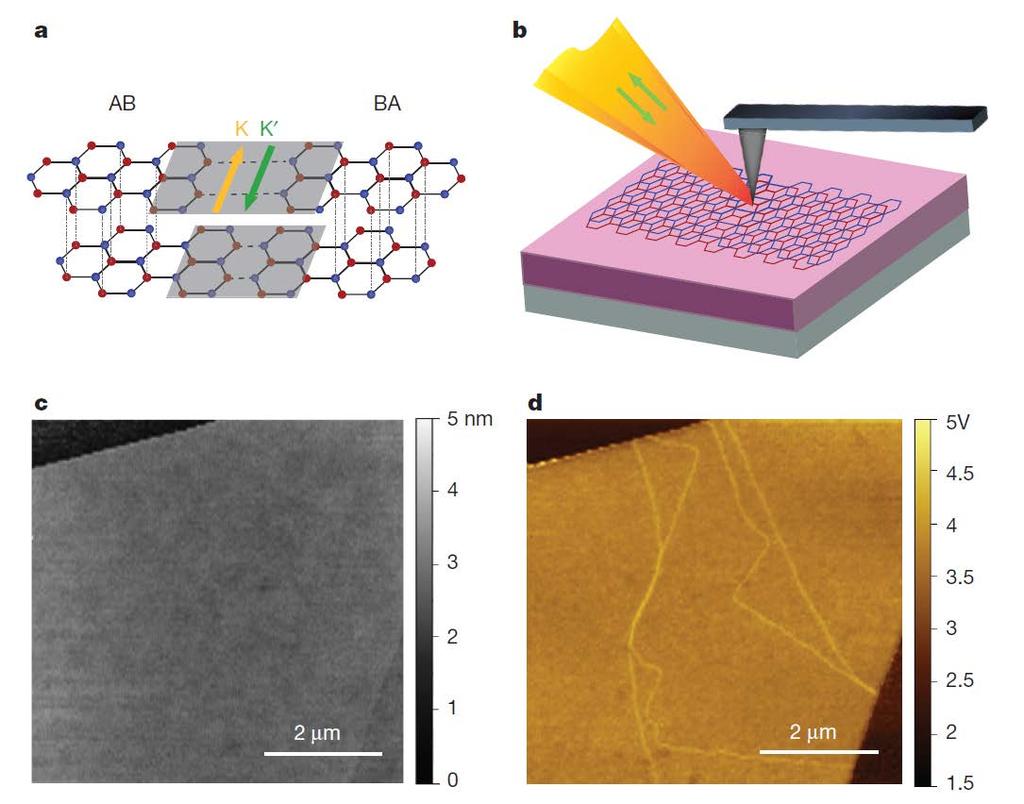

15 Propagation 1-D Transport Channel Along the Domain Boundaries

16 Controlled Stacking of Graphene-Graphene Layers Controlling Twisting Angle: Tear and Stack Integrate with SiN membrane for TEM study Y. Cao et al., (PRL in press)


 Image plane")

17 Dark Field Imaging Graphene Moire Transmission Electron Microscopy Instrument and ray diagram Incommensurate Moire structures Graphene/hBN Graphene/graphene Dark field imaging Graphene/graphene/hBN aperture Specimen Objective lens Back focal plane (Diffraction) Image plane (Real space image) J. M. Yuk et al., Carbon 80, 755 (2014) Dark field imaging Commensurate Moire structures??

")


18 Graphene on Graphene With a Small Twisting Angle TEM dark field image (g = ) and selected area electron diffraction pattern Rotational displacement Uniaxial displacement + =


19 Twisting Engineering C/IC Domain Boundaries

20 Twisted Bilayer Graphene: Satellite Diffraction Peaks TEM diffraction pattern Two graphene sheets with twist Angle: 0.41 deg on hbn substrate 2110 First Order Bragg Peak BN graphene Second Order Bragg Peak Third Order Bragg Peak 12 10


21 Real Space Versus Fourier Space: Satellite Peaks deg 0.41deg 0.79deg 1.6deg Selected Area Diffraction patterns zoomed up (x50) on each graphene peak deg 0.41deg 0.79deg 1.6deg


22 Twisting Angle Dependent Satellite Peak Intensities First Order: Second Order: Third Order: I satellite / I Bragg Satellites 1 Satellites 2 Satellites 1 Satellites 2 Satellite 1 Main Main Satellites 2 Main


23 Relaxation of Atomic Lattice and Buckling Atomic scale relaxation Buckling out of plane Electronic properties.. Wijk et al., Nano Letters (2016)

 and Kolmogorov Crespi (KC)")

24 Atomic Scale Relaxation Modeling: Commensurate Lattice vdw interactions modeled using discrete continuum effective potentials for Lennard Jones (LJ) and Kolmogorov Crespi (KC) for full atomistic resolution. Simulated Diffractions A/B B/A Qualitative agreement with experiments!


25 Mathematical Modeling: Inversion Problem How we can model general incommensurate twisted lattices? Can we recover the microscopic relaxation pattern from satellite diffraction? AB/BA Symmetric AB/BA Asymmetric Paul Cazeaux and Mitch Luskin


 Vertical")

26 Transport Along Domain Boundaries: Topological Mode AC AB AB stack R Q = h/4e 2 AA AC stack Bernal stacking L. Ju et al., Nature 520, 650 (2015) Vertical electric field Bulk energy band Network resistivity ~ h/4e 2 = 6.4 kω


27 Transport at the Neutrality of Twisted Bilayers 2 µm 0 o 3 o Decoupled stacking Bernal stacking V top =+5 V V top =-5 V V top =+10 V V top =-10 V IC/C domains 0.8 o V top =+5 V V top =-5 V


28 Twisting Engineering C/IC Domain Boundaries in MoS 2 S Mo Bulk Stacking Method Controlling Twisting Angle: Tear and Stack Y. Cao et al., (PRL 2016)


29 MoS 2 on MoS 2 With a Small Twisting Angle MoS MoS AB stack with partial dislocations


30 MoS 2 on MoS 2 With 180 o Twisting Angle MoS MoS Pairs of partial dislocations
31 Summary and Outlook Commensuration and incommensuration between electric potential and magnetic length creates fractalized quantum Hall effect C/IC phase transition in CDW lattice in TaS2 can be tuned by dimensionality changes in the samples. In graphene bilayer, tunable domain structures of C/IC boundary can be controlled with twist angle control. Observation of different types of domain structures in bilayer MoS2 formed as a result of commensurate transition. Going Forward: Symmetry elements in the materials can be engineered by twist angle control. Can we generate topologically non-trivial electronic structures from twisted vdw stacks?


32 Acknowledgements Hofstadter Butterfly C. R. Dean, L. Wang, P. Maher, C. Forsythe, F. Ghahari, Y. Gao, J. Katoch, M. Ishigami, P. Moon, M. Koshino, T. Taniguchi, K. Watanabe, K. L. Shepard, J. Hone, Charge Density Waves in TaS 2 A. W. Tsen, R. Hovden, D. Z. Wang, Y. D. Kim, J. Okamoto, K. A. Spoth, Y. Liu, W. J. Lu, Y. P. Sun, J. Hone, L. F. Kourkoutis, and A. N. Pasupathy Twisted vdw Layers H. Yoo, R. Engelke, M. Kim, G. C, Yi K. Zhang, E. Tadmor P. Cazeaux, M. Luskin R. Hovden Funding:
Bloch, Landau, and Dirac: Hofstadter s Butterfly in Graphene. Philip Kim. Physics Department, Columbia University
 Bloch, Landau, and Dirac: Hofstadter s Butterfly in Graphene Philip Kim Physics Department, Columbia University Acknowledgment Prof. Cory Dean (now at CUNY) Lei Wang Patrick Maher Fereshte Ghahari Carlos
SUPPLEMENTARY INFORMATION
 doi:1.138/nature12186 S1. WANNIER DIAGRAM B 1 1 a φ/φ O 1/2 1/3 1/4 1/5 1 E φ/φ O n/n O 1 FIG. S1: Left is a cartoon image of an electron subjected to both a magnetic field, and a square periodic lattice.
Coulomb Drag in Graphene
 Graphene 2017 Coulomb Drag in Graphene -Toward Exciton Condensation Philip Kim Department of Physics, Harvard University Coulomb Drag Drag Resistance: R D = V 2 / I 1 Onsager Reciprocity V 2 (B)/ I 1 =
TOPOLOGICAL BANDS IN GRAPHENE SUPERLATTICES
 TOPOLOGICAL BANDS IN GRAPHENE SUPERLATTICES 1) Berry curvature in superlattice bands 2) Energy scales for Moire superlattices 3) Spin-Hall effect in graphene Leonid Levitov (MIT) @ ISSP U Tokyo MIT Manchester
Supplemental material for Effect of structural relaxation on the electronic structure of graphene on hexagonal boron nitride
 Supplemental material for Effect of structural relaxation on the electronic structure of graphene on hexagonal boron nitride G.J. Slotman, 1 M.M. van Wijk, 1 Pei-Liang Zhao, 2 A. Fasolino, 1 M.I. Katsnelson,
Dislocation network structures in 2D bilayer system
 Dislocation network structures in 2D bilayer system Shuyang DAI School of Mathematics and Statistics Wuhan University Joint work with: Prof. Yang XIANG, HKUST Prof. David SROLOVITZ, UPENN S. Dai IMS Workshop,
Atomic reconstruction at van der Waals interface in twisted bilayer graphene
 Atomic reconstruction at van der Waals interface in twisted bilayer graphene Hyobin Yoo 1, Kuan Zhang 2, Rebecca Engelke 1, Paul Cazeaux 3, Suk Hyun Sung 4, Robert Hovden 4, Adam W. Tsen 5, Takashi Taniguchi
Topological Defects in the Topological Insulator
 Topological Defects in the Topological Insulator Ashvin Vishwanath UC Berkeley arxiv:0810.5121 YING RAN Frank YI ZHANG Quantum Hall States Exotic Band Topology Topological band Insulators (quantum spin
Physics in two dimensions in the lab
 Physics in two dimensions in the lab Nanodevice Physics Lab David Cobden PAB 308 Collaborators at UW Oscar Vilches (Low Temperature Lab) Xiaodong Xu (Nanoscale Optoelectronics Lab) Jiun Haw Chu (Quantum
Supplementary Figure 1. Magneto-transport characteristics of topological semimetal Cd 3 As 2 microribbon. (a) Measured resistance (R) as a function
 Measured resistance (R) as a function") Supplementary Figure 1. Magneto-transport characteristics of topological semimetal Cd 3 As 2 microribbon. (a) Measured resistance (R) as a function of temperature (T) at zero magnetic field. (b) Magnetoresistance
Supplementary Figure 1. Magneto-transport characteristics of topological semimetal Cd 3 As 2 microribbon. (a) Measured resistance (R) as a function of temperature (T) at zero magnetic field. (b) Magnetoresistance
BIASED TWISTED BILAYER GRAPHENE: MAGNETISM AND GAP
 BIASED TWISTED BILAYER GRAPHENE: MAGNETISM AND GAP A.V. Rozhkov, A.O. Sboychakov, A.L. Rakhmanov, F. Nori ITAE RAS, Moscow, Russia RIKEN, Wako-shi, Japan Presentation outline: General properties of twisted
Spin Superfluidity and Graphene in a Strong Magnetic Field
 Spin Superfluidity and Graphene in a Strong Magnetic Field by B. I. Halperin Nano-QT 2016 Kyiv October 11, 2016 Based on work with So Takei (CUNY), Yaroslav Tserkovnyak (UCLA), and Amir Yacoby (Harvard)
Valley Hall effect in electrically spatial inversion symmetry broken bilayer graphene
 NPSMP2015 Symposium 2015/6/11 Valley Hall effect in electrically spatial inversion symmetry broken bilayer graphene Yuya Shimazaki 1, Michihisa Yamamoto 1, 2, Ivan V. Borzenets 1, Kenji Watanabe 3, Takashi
Quantum dynamics in many body systems
 Quantum dynamics in many body systems Eugene Demler Harvard University Collaborators: David Benjamin (Harvard), Israel Klich (U. Virginia), D. Abanin (Perimeter), K. Agarwal (Harvard), E. Dalla Torre (Harvard)
Electronic bands of twisted graphene layers
 Journal Club for Condensed Matter Physics https://www.condmatjclub.org JCCM November 2018 03 Electronic bands of twisted graphene layers 1. Origin of Mott Insulating Behavior and Superconductivity in Twisted
SUPPLEMENTARY INFORMATION
 DOI: 1.138/NMAT3449 Topological crystalline insulator states in Pb 1 x Sn x Se Content S1 Crystal growth, structural and chemical characterization. S2 Angle-resolved photoemission measurements at various
NONLOCAL TRANSPORT IN GRAPHENE: VALLEY CURRENTS, HYDRODYNAMICS AND ELECTRON VISCOSITY
 NONLOCAL TRANSPORT IN GRAPHENE: VALLEY CURRENTS, HYDRODYNAMICS AND ELECTRON VISCOSITY Leonid Levitov (MIT) Frontiers of Nanoscience ICTP Trieste, August, 2015 Boris @ 60 2 Boris @ 60 3 Boris Blinks the
2D Materials with Strong Spin-orbit Coupling: Topological and Electronic Transport Properties
 2D Materials with Strong Spin-orbit Coupling: Topological and Electronic Transport Properties Artem Pulkin California Institute of Technology (Caltech), Pasadena, CA 91125, US Institute of Physics, Ecole
SUPPLEMENTARY INFORMATION
 In the format provided by the authors and unedited. DOI: 10.1038/NPHYS3968 Topological mosaic in Moiré superlattices of van der Waals heterobilayers Qingjun Tong 1, Hongyi Yu 1, Qizhong Zhu 1, Yong Wang
Tunable Moiré Bands and Strong Correlations in Small-Twist-Angle Bilayer Graphene
 Tunable Moiré Bands and Strong Correlations in Small-Twist-Angle Bilayer Graphene Authors: Kyounghwan Kim 1, Ashley DaSilva 2, Shengqiang Huang 3, Babak Fallahazad 1, Stefano Larentis 1, Takashi Taniguchi
Supplementary Figures
 Supplementary Figures Supplementary Figure 1. Crystal structure of 1T -MoTe 2. (a) HAADF-STEM image of 1T -MoTe 2, looking down the [001] zone (scale bar, 0.5 nm). The area indicated by the red rectangle
Topological Defects inside a Topological Band Insulator
 Topological Defects inside a Topological Band Insulator Ashvin Vishwanath UC Berkeley Refs: Ran, Zhang A.V., Nature Physics 5, 289 (2009). Hosur, Ryu, AV arxiv: 0908.2691 Part 1: Outline A toy model of
Zero-bias conductance peak in detached flakes of superconducting 2H-TaS2 probed by STS
 Zero-bias conductance peak in detached flakes of superconducting 2H-TaS2 probed by STS J. A. Galvis, L. C., I. Guillamon, S. Vieira, E. Navarro-Moratalla, E. Coronado, H. Suderow, F. Guinea Laboratorio
SUPPLEMENTARY INFORMATION
 SUPPLEMENTARY INFORMATION SUPPLEMENTARY INFORMATION Trilayer graphene is a semimetal with a gate-tuneable band overlap M. F. Craciun, S. Russo, M. Yamamoto, J. B. Oostinga, A. F. Morpurgo and S. Tarucha
Graphene and Carbon Nanotubes
 Graphene and Carbon Nanotubes 1 atom thick films of graphite atomic chicken wire Novoselov et al - Science 306, 666 (004) 100μm Geim s group at Manchester Novoselov et al - Nature 438, 197 (005) Kim-Stormer
SUPPLEMENTARY INFORMATION
 Dirac electron states formed at the heterointerface between a topological insulator and a conventional semiconductor 1. Surface morphology of InP substrate and the device Figure S1(a) shows a 10-μm-square
A BIT OF MATERIALS SCIENCE THEN PHYSICS
 GRAPHENE AND OTHER D ATOMIC CRYSTALS Andre Geim with many thanks to K. Novoselov, S. Morozov, D. Jiang, F. Schedin, I. Grigorieva, J. Meyer, M. Katsnelson A BIT OF MATERIALS SCIENCE THEN PHYSICS CARBON
Magnetic fields and lattice systems
 Magnetic fields and lattice systems Harper-Hofstadter Hamiltonian Landau gauge A = (0, B x, 0) (homogeneous B-field). Transition amplitude along x gains y-dependence: J x J x e i a2 B e y = J x e i Φy
Stripes developed at the strong limit of nematicity in FeSe film
 Stripes developed at the strong limit of nematicity in FeSe film Wei Li ( ) Department of Physics, Tsinghua University IASTU Seminar, Sep. 19, 2017 Acknowledgements Tsinghua University Prof. Qi-Kun Xue,
Distribution of Chern number by Landau level broadening in Hofstadter butterfly
 Journal of Physics: Conference Series PAPER OPEN ACCESS Distribution of Chern number by Landau level broadening in Hofstadter butterfly To cite this article: Nobuyuki Yoshioka et al 205 J. Phys.: Conf.
SUPPLEMENTARY INFORMATION. Observation of tunable electrical bandgap in large-area twisted bilayer graphene synthesized by chemical vapor deposition
 SUPPLEMENTARY INFORMATION Observation of tunable electrical bandgap in large-area twisted bilayer graphene synthesized by chemical vapor deposition Jing-Bo Liu 1 *, Ping-Jian Li 1 *, Yuan-Fu Chen 1, Ze-Gao
Symmetry Protected Topological Insulators and Semimetals
 Symmetry Protected Topological Insulators and Semimetals I. Introduction : Many examples of topological band phenomena II. Recent developments : - Line node semimetal Kim, Wieder, Kane, Rappe, PRL 115,
single-layer transition metal dichalcogenides MC2
 single-layer transition metal dichalcogenides MC2 Period 1 1 H 18 He 2 Group 1 2 Li Be Group 13 14 15 16 17 18 B C N O F Ne 3 4 Na K Mg Ca Group 3 4 5 6 7 8 9 10 11 12 Sc Ti V Cr Mn Fe Co Ni Cu Zn Al Ga
Direct imaging of topological edge states at a bilayer graphene domain wall
 Direct imaging of topological edge states at a bilayer graphene domain wall Long-Jing Yin 1, Hua Jiang 2, Jia-Bin Qiao 1, Lin He 1, * 1 Center for Advanced Quantum Studies, Department of Physics, Beijing
Phase Change and Piezoelectric Properties of Two-Dimensional Materials
 Phase Change and Piezoelectric Properties of Two-Dimensional Materials April 22, 2015 Karel-Alexander Duerloo, Yao Li, Yao Zhou, Evan Reed Department of Materials Science and Engineering Stanford University
van der Waals Heterostructures: Fabrication and Materials Issues
 van der Waals Heterostructures: Fabrication and Materials Issues J. Hone Columbia University Mechanical Engineering Center for Precision Assembly of Superstratic and Superatomic Solids (PAS 3 ) Columbia
Observation of topological surface state quantum Hall effect in an intrinsic three-dimensional topological insulator
 Observation of topological surface state quantum Hall effect in an intrinsic three-dimensional topological insulator Authors: Yang Xu 1,2, Ireneusz Miotkowski 1, Chang Liu 3,4, Jifa Tian 1,2, Hyoungdo
Overview. Carbon in all its forms. Background & Discovery Fabrication. Important properties. Summary & References. Overview of current research
 Graphene Prepared for Solid State Physics II Pr Dagotto Spring 2009 Laurene Tetard 03/23/09 Overview Carbon in all its forms Background & Discovery Fabrication Important properties Overview of current
Vortex States in a Non-Abelian Magnetic Field
 Vortex States in a Non-Abelian Magnetic Field Predrag Nikolić George Mason University Institute for Quantum Matter @ Johns Hopkins University SESAPS November 10, 2016 Acknowledgments Collin Broholm IQM
Graphite, graphene and relativistic electrons
 Graphite, graphene and relativistic electrons Introduction Physics of E. graphene Y. Andrei Experiments Rutgers University Transport electric field effect Quantum Hall Effect chiral fermions STM Dirac
Dirac fermions in Graphite:
 Igor Lukyanchuk Amiens University, France, Yakov Kopelevich University of Campinas, Brazil Dirac fermions in Graphite: I. Lukyanchuk, Y. Kopelevich et al. - Phys. Rev. Lett. 93, 166402 (2004) - Phys. Rev.
Center for Integrated Nanostructure Physics (CINAP)
") Center for Integrated Nanostructure Physics (CINAP) - Institute for Basic Science (IBS) was launched in 2012 by the Korean government to promote basic science in Korea - Our Center was established in 2012
Center for Integrated Nanostructure Physics (CINAP) - Institute for Basic Science (IBS) was launched in 2012 by the Korean government to promote basic science in Korea - Our Center was established in 2012
Quantum anomalous Hall states on decorated magnetic surfaces
 Quantum anomalous Hall states on decorated magnetic surfaces David Vanderbilt Rutgers University Kevin Garrity & D.V. Phys. Rev. Lett.110, 116802 (2013) Recently: Topological insulators (TR-invariant)
Quantum Hall effect. Quantization of Hall resistance is incredibly precise: good to 1 part in I believe. WHY?? G xy = N e2 h.
 Quantum Hall effect V1 V2 R L I I x = N e2 h V y V x =0 G xy = N e2 h n.b. h/e 2 = 25 kohms Quantization of Hall resistance is incredibly precise: good to 1 part in 10 10 I believe. WHY?? Robustness Why
Notes on Topological Insulators and Quantum Spin Hall Effect. Jouko Nieminen Tampere University of Technology.
 Notes on Topological Insulators and Quantum Spin Hall Effect Jouko Nieminen Tampere University of Technology. Not so much discussed concept in this session: topology. In math, topology discards small details
Band Structure Engineering of 2D materials using Patterned Dielectric Superlattices
 Band Structure Engineering of 2D materials using Patterned Dielectric Superlattices Carlos Forsythe 1, Xiaodong Zhou 1,2, Takashi Taniguchi 3, Kenji Watanabe 3, Abhay Pasupathy 1, Pilkyung Moon 4, Mikito
SECOND PUBLIC EXAMINATION. Honour School of Physics Part C: 4 Year Course. Honour School of Physics and Philosophy Part C C3: CONDENSED MATTER PHYSICS
 A11046W1 SECOND PUBLIC EXAMINATION Honour School of Physics Part C: 4 Year Course Honour School of Physics and Philosophy Part C C3: CONDENSED MATTER PHYSICS TRINITY TERM 2015 Wednesday, 17 June, 2.30
Anomalous Metals and Failed Superconductors. With B. Spivak and A. Kapitulnik (also P. Oreto)
") Anomalous Metals and Failed Superconductors With B. Spivak and A. Kapitulnik (also P. Oreto) Tallahassee 2018 Pillars the Theory of Quantum Mater From B Spivak Α proof of the Fermi liquid theory is based
Anomalous Metals and Failed Superconductors With B. Spivak and A. Kapitulnik (also P. Oreto) Tallahassee 2018 Pillars the Theory of Quantum Mater From B Spivak Α proof of the Fermi liquid theory is based
Nanostructured Carbon Allotropes as Weyl-Like Semimetals
 Nanostructured Carbon Allotropes as Weyl-Like Semimetals Shengbai Zhang Department of Physics, Applied Physics & Astronomy Rensselaer Polytechnic Institute symmetry In quantum mechanics, symmetry can be
Mesoscopic superlattices
 Mesoscopic superlattices Mesoscopic superlattices Periodic arrays of mesoscopic elements. Lateral superlattices can be imposed onto a 2DEG by lithographic techniques. One-dimensional superlattices Patterned
Landau Quantization in Graphene Monolayer, Bernal Bilayer, and Bernal
 Landau Quantization in Graphene Monolayer, Bernal Bilayer, and Bernal Trilayer on Graphite Surface Long-Jing Yin, Si-Yu Li, Jia-Bin Qiao, Jia-Cai Nie, Lin He * Electronic properties of surface areas decoupled
Floquet theory of photo-induced topological phase transitions: Application to graphene
 Floquet theory of photo-induced topological phase transitions: Application to graphene Takashi Oka (University of Tokyo) T. Kitagawa (Harvard) L. Fu (Harvard) E. Demler (Harvard) A. Brataas (Norweigian
Topological insulator (TI)
") Topological insulator (TI) Haldane model: QHE without Landau level Quantized spin Hall effect: 2D topological insulators: Kane-Mele model for graphene HgTe quantum well InAs/GaSb quantum well 3D topological
Topological insulator (TI) Haldane model: QHE without Landau level Quantized spin Hall effect: 2D topological insulators: Kane-Mele model for graphene HgTe quantum well InAs/GaSb quantum well 3D topological
Supplementary Figure S1. STM image of monolayer graphene grown on Rh (111). The lattice
. The lattice") Supplementary Figure S1. STM image of monolayer graphene grown on Rh (111). The lattice mismatch between graphene (0.246 nm) and Rh (111) (0.269 nm) leads to hexagonal moiré superstructures with the expected
Supplementary Figure S1. STM image of monolayer graphene grown on Rh (111). The lattice mismatch between graphene (0.246 nm) and Rh (111) (0.269 nm) leads to hexagonal moiré superstructures with the expected
Nuclear spin spectroscopy for semiconductor hetero and nano structures
 (Interaction and Nanostructural Effects in Low-Dimensional Systems) November 16th, Kyoto, Japan Nuclear spin spectroscopy for semiconductor hetero and nano structures Yoshiro Hirayama Tohoku University
The Quantum Spin Hall Effect
 The Quantum Spin Hall Effect Shou-Cheng Zhang Stanford University with Andrei Bernevig, Taylor Hughes Science, 314,1757 2006 Molenamp et al, Science, 318, 766 2007 XL Qi, T. Hughes, SCZ preprint The quantum
What is a topological insulator? Ming-Che Chang Dept of Physics, NTNU
 What is a topological insulator? Ming-Che Chang Dept of Physics, NTNU A mini course on topology extrinsic curvature K vs intrinsic (Gaussian) curvature G K 0 G 0 G>0 G=0 K 0 G=0 G
Disordered topological insulators with time-reversal symmetry: Z 2 invariants
 Keio Topo. Science (2016/11/18) Disordered topological insulators with time-reversal symmetry: Z 2 invariants Hosho Katsura Department of Physics, UTokyo Collaborators: Yutaka Akagi (UTokyo) Tohru Koma
Carbon based Nanoscale Electronics
 Carbon based Nanoscale Electronics 09 02 200802 2008 ME class Outline driving force for the carbon nanomaterial electronic properties of fullerene exploration of electronic carbon nanotube gold rush of
SUPPLEMENTARY INFORMATION
 A Dirac point insulator with topologically non-trivial surface states D. Hsieh, D. Qian, L. Wray, Y. Xia, Y.S. Hor, R.J. Cava, and M.Z. Hasan Topics: 1. Confirming the bulk nature of electronic bands by
2D MBE Activities in Sheffield. I. Farrer, J. Heffernan Electronic and Electrical Engineering The University of Sheffield
 2D MBE Activities in Sheffield I. Farrer, J. Heffernan Electronic and Electrical Engineering The University of Sheffield Outline Motivation Van der Waals crystals The Transition Metal Di-Chalcogenides
Fermi polaron-polaritons in MoSe 2
 Fermi polaron-polaritons in MoSe 2 Meinrad Sidler, Patrick Back, Ovidiu Cotlet, Ajit Srivastava, Thomas Fink, Martin Kroner, Eugene Demler, Atac Imamoglu Quantum impurity problem Nonperturbative interaction
Topological Kondo Insulator SmB 6. Tetsuya Takimoto
 Topological Kondo Insulator SmB 6 J. Phys. Soc. Jpn. 80 123720, (2011). Tetsuya Takimoto Department of Physics, Hanyang University Collaborator: Ki-Hoon Lee (POSTECH) Content 1. Introduction of SmB 6 in-gap
Vortices and vortex states of Rashba spin-orbit coupled condensates
 Vortices and vortex states of Rashba spin-orbit coupled condensates Predrag Nikolić George Mason University Institute for Quantum Matter @ Johns Hopkins University March 5, 2014 P.N, T.Duric, Z.Tesanovic,
arxiv: v1 [cond-mat.mes-hall] 1 Nov 2011
![arxiv: v1 [cond-mat.mes-hall] 1 Nov 2011](/thumbs/93/111880633.jpg "arxiv: v1 [cond-mat.mes-hall] 1 Nov 2011") V The next nearest neighbor effect on the D materials properties Maher Ahmed Department of Physics and Astronomy, University of Western Ontario, London ON N6A K7, Canada and arxiv:.v [cond-mat.mes-hall]
V The next nearest neighbor effect on the D materials properties Maher Ahmed Department of Physics and Astronomy, University of Western Ontario, London ON N6A K7, Canada and arxiv:.v [cond-mat.mes-hall]
New Quantum Transport Results in Type-II InAs/GaSb Quantum Wells
 New Quantum Transport Results in Type-II InAs/GaSb Quantum Wells Wei Pan Sandia National Laboratories Sandia National Laboratories is a multi-program laboratory managed and operated by Sandia Corporation,
Monolayer Semiconductors
 Monolayer Semiconductors Gilbert Arias California State University San Bernardino University of Washington INT REU, 2013 Advisor: Xiaodong Xu (Dated: August 24, 2013) Abstract Silicon may be unable to
Effects of Interactions in Suspended Graphene
 Effects of Interactions in Suspended Graphene Ben Feldman, Andrei Levin, Amir Yacoby, Harvard University Broken and unbroken symmetries in the lowest LL: spin and valley symmetries. FQHE Discussions with
Impact of disorder and topology in two dimensional systems at low carrier densities
 Impact of disorder and topology in two dimensional systems at low carrier densities A Thesis Submitted For the Degree of Doctor of Philosophy in the Faculty of Science by Mohammed Ali Aamir Department
Supplementary Figure 1 Magneto-transmission spectra of graphene/h-bn sample 2 and Landau level transition energies of three other samples.
 Supplementary Figure 1 Magneto-transmission spectra of graphene/h-bn sample 2 and Landau level transition energies of three other samples. (a,b) Magneto-transmission ratio spectra T(B)/T(B 0 ) of graphene/h-bn
Magneto-plasmonic effects in epitaxial graphene
 Magneto-plasmonic effects in epitaxial graphene Alexey Kuzmenko University of Geneva Graphene Nanophotonics Benasque, 4 March 13 Collaborators I. Crassee, N. Ubrig, I. Nedoliuk, J. Levallois, D. van der
Spin-orbit proximity effects in graphene on TMDCs. Jaroslav Fabian
 Hvar, 4.10.2017 Spin-orbit proximity effects in graphene on TMDCs Jaroslav Fabian Institute for Theoretical Physics University of Regensburg SFB1277 GRK TI SPP 1666 SFB689 GRK1570 SPP 1538 Arbeitsgruppe
Spin correlations in conducting and superconducting materials Collin Broholm Johns Hopkins University
 Spin correlations in conducting and superconducting materials Collin Broholm Johns Hopkins University Supported by U.S. DoE Basic Energy Sciences, Materials Sciences & Engineering DE-FG02-08ER46544 Overview
Supplementary Information
 Supplementary Information Supplementary Figure S1: Ab initio band structures in presence of spin-orbit coupling. Energy bands for (a) MoS 2, (b) MoSe 2, (c) WS 2, and (d) WSe 2 bilayers. It is worth noting
Supplementary Figure 1. Selected area electron diffraction (SAED) of bilayer graphene and tblg. (a) AB
 of bilayer graphene and tblg. (a) AB") Supplementary Figure 1. Selected area electron diffraction (SAED) of bilayer graphene and tblg. (a) AB stacked bilayer graphene (b), (c), (d), (e), and (f) are twisted bilayer graphene with twist angle
Supplementary Figure 1. Selected area electron diffraction (SAED) of bilayer graphene and tblg. (a) AB stacked bilayer graphene (b), (c), (d), (e), and (f) are twisted bilayer graphene with twist angle
Contact Engineering of Two-Dimensional Layered Semiconductors beyond Graphene
 Contact Engineering of Two-Dimensional Layered Semiconductors beyond Graphene Zhixian Zhou Department of Physics and Astronomy Wayne State University Detroit, Michigan Outline Introduction Ionic liquid
Pseudospin Soliton in the ν=1 Bilayer Quantum Hall State. A. Sawada. Research Center for Low Temperature and Materials Sciences Kyoto University
 YKIS2007, Sawada Pseudospin Soliton in the ν=1 Bilayer Quantum Hall State A. Sawada Research Center for Low Temperature and Materials Sciences Kyoto University Collaborators Fukuda (Kyoto Univ.) K. Iwata
Multiwalled nanotube faceting unravelled
 Multiwalled nanotube faceting unravelled Itai Leven, Roberto Guerra, Andrea Vanossi, Erio Tosatti, and Oded Hod NATURE NANOTECHNOLOGY www.nature.com/naturenanotechnology 1 1. Achiral DWCNTs optimized using
Scanning gate microscopy and individual control of edge-state transmission through a quantum point contact
 Scanning gate microscopy and individual control of edge-state transmission through a quantum point contact Stefan Heun NEST, CNR-INFM and Scuola Normale Superiore, Pisa, Italy Coworkers NEST, Pisa, Italy:
Trajectory of the anomalous Hall effect towards the quantized state in a ferromagnetic topological insulator
 Trajectory of the anomalous Hall effect towards the quantized state in a ferromagnetic topological insulator J. G. Checkelsky, 1, R. Yoshimi, 1 A. Tsukazaki, 2 K. S. Takahashi, 3 Y. Kozuka, 1 J. Falson,
Topological Heterostructures by Molecular Beam Epitaxy
 Topological Heterostructures by Molecular Beam Epitaxy Susanne Stemmer Materials Department, University of California, Santa Barbara Fine Lecture, Northwestern University February 20, 2018 Stemmer Group
Let There Be Topological Superconductors
 Let There Be Topological Superconductors K K d Γ ~q c µ arxiv:1606.00857 arxiv:1603.02692 Eun-Ah Kim (Cornell) Boulder 7.21-22.2016 Q. Topological Superconductor material? Bulk 1D proximity 2D proximity?
Emergent topological phenomena in antiferromagnets with noncoplanar spins
 Emergent topological phenomena in antiferromagnets with noncoplanar spins - Surface quantum Hall effect - Dimensional crossover Bohm-Jung Yang (RIKEN, Center for Emergent Matter Science (CEMS), Japan)
Chiral Majorana fermion from quantum anomalous Hall plateau transition
 Chiral Majorana fermion from quantum anomalous Hall plateau transition Phys. Rev. B, 2015 王靖复旦大学物理系 wjingphys@fudan.edu.cn Science, 2017 1 Acknowledgements Stanford Biao Lian Quan Zhou Xiao-Liang Qi Shou-Cheng
Dirac matter: Magneto-optical studies
 Dirac matter: Magneto-optical studies Marek Potemski Laboratoire National des Champs Magnétiques Intenses Grenoble High Magnetic Field Laboratory CNRS/UGA/UPS/INSA/EMFL MOMB nd International Conference
The twisted bilayer: an experimental and theoretical review. Graphene, 2009 Benasque. J.M.B. Lopes dos Santos
 Moiré in Graphite and FLG Continuum theory Results Experimental and theoretical conrmation Magnetic Field The twisted bilayer: an experimental and theoretical review J.M.B. Lopes dos Santos CFP e Departamento
Direct Observation of Mono-, Bi-, and Tri-layer Charge Density Waves in 1T-TaS 2 by Transmission Electron Microscopy without a Substrate
 Direct Observation of Mono-, Bi-, and Tri-layer Charge Density Waves in 1T-TaS 2 by Transmission Electron Microscopy without a Substrate Daiki Sakabe 1,2, Zheng Liu 3,4, Kazumoto Suenaga 2,4, Keiji Nakatsugawa
Experimental reconstruction of the Berry curvature in a topological Bloch band
 Experimental reconstruction of the Berry curvature in a topological Bloch band Christof Weitenberg Workshop Geometry and Quantum Dynamics Natal 29.10.2015 arxiv:1509.05763 (2015) Topological Insulators
Protection of the surface states of a topological insulator: Berry phase perspective
 Protection of the surface states of a topological insulator: Berry phase perspective Ken-Ichiro Imura Hiroshima University collaborators: Yositake Takane Tomi Ohtsuki Koji Kobayashi Igor Herbut Takahiro
Topological Insulators
 Topological Insulators A new state of matter with three dimensional topological electronic order L. Andrew Wray Lawrence Berkeley National Lab Princeton University Surface States (Topological Order in
Weak-Beam Dark-Field Technique
 Basic Idea recall bright-field contrast of dislocations: specimen close to Bragg condition, s î 0 Weak-Beam Dark-Field Technique near the dislocation core, some planes curved to s = 0 ) strong Bragg reflection
Quantum Hall effect and Landau level crossing of Dirac fermions in trilayer graphene Supplementary Information
 Quantum Hall effect and Landau level crossing of Dirac fermions in trilayer graphene Supplementary Information Thiti Taychatanapat, Kenji Watanabe, Takashi Taniguchi, Pablo Jarillo-Herrero Department of
Impurities and graphene hybrid structures: insights from first-principles theory
 Impurities and graphene hybrid structures: insights from first-principles theory Tim Wehling Institute for Theoretical Physics and Bremen Center for Computational Materials Science University of Bremen
Topological Kondo Insulators!
 Topological Kondo Insulators! Maxim Dzero, University of Maryland Collaborators: Kai Sun, University of Maryland Victor Galitski, University of Maryland Piers Coleman, Rutgers University Main idea Kondo
Tunable Band Gap of Silicene on Monolayer Gallium Phosphide Substrate
 2017 International Conference on Energy Development and Environmental Protection (EDEP 2017) ISBN: 978-1-60595-482-0 Tunable Band Gap of Silicene on Monolayer Gallium Phosphide Substrate Miao-Juan REN
Luttinger Liquid at the Edge of a Graphene Vacuum
 Luttinger Liquid at the Edge of a Graphene Vacuum H.A. Fertig, Indiana University Luis Brey, CSIC, Madrid I. Introduction: Graphene Edge States (Non-Interacting) II. III. Quantum Hall Ferromagnetism and
Quantum Quenches in Chern Insulators
 Quantum Quenches in Chern Insulators Nigel Cooper Cavendish Laboratory, University of Cambridge CUA Seminar M.I.T., November 10th, 2015 Marcello Caio & Joe Bhaseen (KCL), Stefan Baur (Cambridge) M.D. Caio,
Physics in Quasi-2D Materials for Spintronics Applications
 Physics in Quasi-2D Materials for Spintronics Applications Topological Insulators and Graphene Ching-Tzu Chen IBM TJ Watson Research Center May 13, 2016 2016 C-SPIN Topological Spintronics Device Workshop
High-Resolution. Transmission. Electron Microscopy
 Part 4 High-Resolution Transmission Electron Microscopy 186 Significance high-resolution transmission electron microscopy (HRTEM): resolve object details smaller than 1nm (10 9 m) image the interior of
Topology of the Fermi surface wavefunctions and magnetic oscillations in metals
 Topology of the Fermi surface wavefunctions and magnetic oscillations in metals A. Alexandradinata L.I. Glazman Yale University arxiv:1707.08586, arxiv:1708.09387 + in preparation Physics Next Workshop