Comparison of Ultra-Thin InAs and InGaAs Quantum Wells and Ultra-Thin-Body Surface-Channel MOSFETs
|
|
|
- Junior Dorsey
- 5 years ago
- Views:
Transcription

1 Comparison of Ultra-Thin InAs and InGaAs Quantum Wells and Ultra-Thin-Body Surface-Channel MOSFETs Cheng-Ying Huang 1, Sanghoon Lee 1, Evan Wilson 3, Pengyu Long 3, Michael Povolotskyi 3, Varistha Chobpattana 2, Susanne Stemmer 2, Arthur Gossard 1,2, Gerhard Klimeck 3, and Mark Rodwell 1 1 ECE, University of California, Santa Barbara 2 Materials Department, University of California, Santa Barbara 3 Network for Computational Nanotechnology, Purdue University, West Lafayette, IN CSW/IPRM 2015 Santa Barbara, CA
 must be scaled in proportional to gate")

2 Why III-V FETs? Why Ultra-thin channel? III-V channel: low electron effective mass high velocity, high mobility higher current at lower V DD reducing switching power Channel thickness (T ch ) must be scaled in proportional to gate length (L g ) to maintain electrostatic integrity. For ultra-thin body (UTB) MOSFETs T ch ~1/4 L g, and for FinFETs T ch ~1/2 L g. At 7 or 5 nm nodes, channel thickness should be around 2-4 nm. Goal: Carefully examine InGaAs and InAs channels. The best design?? 300K Si InAs InGaAs m e * μ e (cm 2 /V s) μ h (cm 2 /V s) <300 t Si ~5nm W FIN ~8nm Eg(eV) ε r a(å) (InP) Quantum confinement effects!! STM-Leti-IBM Intel 14nm FinFET 14nm UTBSOI IEDM2014 Makr Bohr, IDF2014 2
: μ InAs μ InGaAs Carrier concentration decreases due to increased E 0.")
3 Ultra-thin channel 2DEG: Hall results Quantum well (QW) 2DEGs were grown by solid source MBE. For wide wells: μ InAs > μ InGaAs For narrow wells (~2 nm): μ InAs μ InGaAs Carrier concentration decreases due to increased E 0. Mobility (cm 2 /Vs) InAs channel InGaAs channel Well Thickness (nm) Carrier concentration(10 12 cm -2 ) InAs channel InGaAs channel Well Thickness (nm) 3
4 What happens in thin wells? Mobility is limited by interface roughness scattering. Strained InAs growth (S-K mode) might induce higher interface roughness. Electron effective mass are similar for ~2-3 nm InAs and InGaAs wells because of non-parabolic band effects. Mobility (cm 2 V -1 s -1 ) InGaAs well alloy µ ~T ch -6 interface roughness remote impurity acoustic phonon polar optical phonon total 300K Well thickness(nm) C. Y. Huang et al., J. Appl. Phys. 115, (2013) In-plane effective mass, m // (m 0 ) InGaAs/InP, Nag1993 InAs/InP, Nag1993 InGaAs/InP, Wetzel1992 InGaAs/InP, Hrivnak1992 InAs, Mugny2015 Schneider1995 Wiesner1994 Wetzel InGaAs 0.03 InAs Well Thickness (nm) J. Appl. Phys. 77, 2828 (1995), Phys. Rev. B, 52, 1038 (1996), Appl. Phys. Lett 64, 2520 (1994), Appl. Phys. Lett 62, 2416 (1993), G. Mugny et al., EUROSOI-ULSI conference
 V GS = -0.2 V to 1.0 V 0.")
5 Ultra-thin body III-V FETs: L g ~40 nm I D (ma/ m) I D (ma/ m) UTB FETs with 3 nm channels were fabricated to compare InAs and InGaAs channels. 1.6:1 I on and transcoaductance for InAs channels. 10:1 lower I off for InGaAs channels = 0.1 to 0.7 V 0.2 V increment InAs V GS (V) V GS = -0.2 V to 1.0 V 0.2 V increment R on = 292 Ohm- m at V GS = 1.0 V InAs V (V) = 0.1 to 0.7 V 0.2 V increment InGaAs V GS (V) V GS = -0.2 V to 1.0 V 0.2 V increment R on = 400 Ohm- m at V GS = 1.0 V InGaAs V (V) gm (ms/ m) 5
6 I on ( A/ m) On-state performance Peak g m (ms/ m) R on (Ohm m) nm InAs 3 nm InGaAs = 0.5 V I off = 100 na/ m Gate length (nm) = 0.5 V 3 nm InAs 3 nm InGaAs Gate length ( m) V GS = 1 V 3 nm InAs 3 nm InGaAs R S/D ~ Ohm m Gate length ( m) Higher I on and higher g m for UTB InAs FETs than InGaAs UTB FETs. InAs FETs achieve g m =2 ms/μm, and I on =400 μa/μm at =0.5V and I off =100 na/μm. Similar source/drain resistance (R S/D ) ensures that the performance degradation of InGaAs is not from source/drain, but from channel itself (slope). 6
7 Subthreshold Swing (mv/dec) Subthreshold swing and off-state current DIBL (mv/v) I OFF, MIN (na/ m) =0.1 V,3 nm InAs =0.5 V,3 nm InAs =0.1 V,3 nm InGaAs =0.5 V,3 nm InGaAs nm InAs 3 nm InGaAs V th at 1 A/ m nm InAs nm InGaAs = 0.5 V Gate Length ( m) Gate length ( m) Gate length (nm) Superior SS~83 mv/dec. and DIBL~110 mv/v because of ultra-thin channels and improved electrostatics. Minimum I off is 10:1 lower for InGaAs channel at short L g, where leakage current limited by band-to-band tunneling. InGaAs FETs are limited by gate leakage at long L g. 7


8 Why QW-2DEGs and UTB-FETs show different results? 1 st possible cause: Electron population in L valley due to strong quantum confinement Unlikely. 2nm InAlAs barrier, 3nm InGaAs channel with H passivation on top 2nm InAlAs barrier, 3nm InAs channel with H passivation on top Courtesy of Evan Wilson, Pengyu Long, Michael Povolotskyi, and Gerhard Klimeck. In 0.53 Ga 0.47 As InAs m e * at Γ [m 0 ] Γ L separation [ev] E g at Γ [ev]

 J. Robertson, Appl. Phys. Lett. 94, 152104 (2009) N.")
9 Why QW-2DEGs and UTB-FETs show different results? 2 nd possible cause: Electron interaction with oxide traps inside conduction band Likely. Electrons in high In% content channels have less scattering and less electron capture by the oxide traps. J. Robertson et al., J. Appl. Phys. 117, (2015) J. Robertson, Appl. Phys. Lett. 94, (2009) N. Taoka et al., Trans. Electron Devices. 13, 456 (2011) N. Taoka et al., IEEE IEDM 2011,
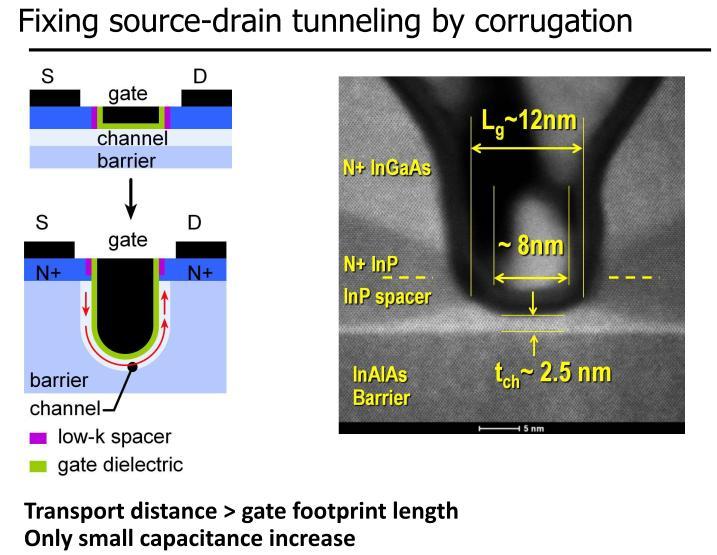
 I D (ma/ m) N+InGaAs N+InP InP spacer L g")


10 UCSB L g ~12 nm III-V MOSFETs (DRC 2015) I D (ma/ m) I D (ma/ m) N+InGaAs N+InP InP spacer L g ~12nm ~ 8nm Ni V GS (V) 1.5 V GS = -0.2 V to 1.2 V 1.0 = 0.1 to 0.7 V, 0.2 V increment SS~107 mv/dec. SS~98 mv/dec. 0.2 V increment R on = 302 Ohm- m at V GS = 1.0 V gm (ms/ m) 0.5 InAlAs Barrier t ch ~ 2.5 nm (1.5/1 nm InGaAs/InAs) (V) I on /I off >
11 Summary Below 10 nm logic nodes, ultrathin channels are required. In QW 2DEGs, the electron Hall mobility are similar for InGaAs and InAs wells as the wells thinned to 2~3nm. In UTB MOSFETs, 3 nm InAs channels significantly improve on-state current and transconductance (~1.6:1), and reduce channel resistance as compared to 3 nm InGaAs channel. Purdue s tight-binding calculations show large ~0.6 ev Γ L splitting in 3 nm InGaAs channels, ruling out the possibility of electron population in L-valley. UCSB C-V measurements show large dispersion in 3 nm InGaAs channels, possibly indicating the significant electron interactions with oxide traps. (As-As anti-bonding may be the culprit) 11

12 Acknowledgment Thanks for your attention! Questions? This research was supported by the SRC Non-classical CMOS Research Center (Task ) and GLOBALFOUNDRIES(Task ). A portion of this work was done in the UCSB nanofabrication facility, part of NSF funded NNIN network. This work was partially supported by the MRSEC Program of the National Science Foundation under Award No. DMR cyhuang@ece.ucsb.edu
13 (backup slides follow)
14 Effective C G ( F/cm 2 ) Mobility (cm 2 /V s) Mobility in different channel design: 25 µm-l g nm InGaAs 2.5 nm InAs 5.0 nm InAs Freq.: 200 khz W/L=25 m/21 m V GS (V) Carrier density ( cm -2 ) nm InGaAs 2.5 nm InAs 5.0 nm InAs Carrier density (cm -2 ) m*, C g-ch, R S/D more important for ballistic FETs
15

16
Performance Analysis of Ultra-Scaled InAs HEMTs
 Purdue University Purdue e-pubs Birck and NCN Publications Birck Nanotechnology Center 2009 Performance Analysis of Ultra-Scaled InAs HEMTs Neerav Kharche Birck Nanotechnology Center and Purdue University,
III-V CMOS: What have we learned from HEMTs? J. A. del Alamo, D.-H. Kim 1, T.-W. Kim, D. Jin, and D. A. Antoniadis
 III-V CMOS: What have we learned from HEMTs? J. A. del Alamo, D.-H. Kim 1, T.-W. Kim, D. Jin, and D. A. Antoniadis Microsystems Technology Laboratories, MIT 1 presently with Teledyne Scientific 23rd International
Ultra-Scaled InAs HEMTs
 Performance Analysis of Ultra-Scaled InAs HEMTs Neerav Kharche 1, Gerhard Klimeck 1, Dae-Hyun Kim 2,3, Jesús. A. del Alamo 2, and Mathieu Luisier 1 1 Network for Computational ti Nanotechnology and Birck
The Prospects for III-Vs
 10 nm CMOS: The Prospects for III-Vs J. A. del Alamo, Dae-Hyun Kim 1, Donghyun Jin, and Taewoo Kim Microsystems Technology Laboratories, MIT 1 Presently with Teledyne Scientific 2010 European Materials
Effect of the High-k Dielectric/Semiconductor Interface on Electronic Properties in Ultra-thin Channels
 Effect of the High-k Dielectric/Semiconductor Interface on Electronic Properties in Ultra-thin Channels Evan Wilson, Daniel Valencia, Mark J. W. Rodwell, Gerhard Klimeck and Michael Povolotskyi Electrical
OMEN an atomistic and full-band quantum transport simulator for post-cmos nanodevices
 Purdue University Purdue e-pubs Other Nanotechnology Publications Birck Nanotechnology Center 8-18-28 OMEN an atomistic and full-band quantum transport simulator for post-cmos nanodevices Mathieu Luisier
Technology Development & Design for 22 nm InGaAs/InP-channel MOSFETs
 2008 Indium Phosphide and Related Materials Conference, May, Versailles, France Technology Development & Design for 22 nm InGaAs/InP-channel MOSFETs M. Rodwell University of California, Santa Barbara M.
Technology Development for InGaAs/InP-channel MOSFETs
 MRS Spring Symposium, Tutorial: Advanced CMOS Substrates, Devices, Reliability, and Characterization, April 13, 2009, San Francisco Technology Development for InGaAs/InP-channel MOSFETs Mark Rodwell University
Microsystems Technology Laboratories, MIT. Teledyne Scientific Company (TSC)
") Extraction of Virtual-Source Injection Velocity in sub-100 nm III-V HFETs 1,2) D.-H. Kim, 1) J. A. del Alamo, 1) D. A. Antoniadis and 2) B. Brar 1) Microsystems Technology Laboratories, MIT 2) Teledyne
Extraction of Virtual-Source Injection Velocity in sub-100 nm III-V HFETs 1,2) D.-H. Kim, 1) J. A. del Alamo, 1) D. A. Antoniadis and 2) B. Brar 1) Microsystems Technology Laboratories, MIT 2) Teledyne
High Mobility Materials and Novel Device Structures for High Performance Nanoscale MOSFETs
 High Mobility Materials and Novel Device Structures for High Performance Nanoscale MOSFETs Prof. (Dr.) Tejas Krishnamohan Department of Electrical Engineering Stanford University, CA & Intel Corporation
InGaAs Double-Gate Fin-Sidewall MOSFET
 InGaAs Double-Gate Fin-Sidewall MOSFET Alon Vardi, Xin Zhao and Jesús del Alamo Microsystems Technology Laboratories, MIT June 25, 214 Sponsors: Sematech, Technion-MIT Fellowship, and NSF E3S Center (#939514)
Carbon Nanotube Electronics
 Carbon Nanotube Electronics Jeorg Appenzeller, Phaedon Avouris, Vincent Derycke, Stefan Heinz, Richard Martel, Marko Radosavljevic, Jerry Tersoff, Shalom Wind H.-S. Philip Wong hspwong@us.ibm.com IBM T.J.
ALD high-k and higher-k integration on GaAs
 ALD high-k and higher-k integration on GaAs Ozhan Koybasi 1), Min Xu 1), Yiqun Liu 2), Jun-Jieh Wang 2), Roy G. Gordon 2), and Peide D. Ye 1)* 1) School of Electrical and Computer Engineering, Purdue University,
The Pennsylvania State University. Kurt J. Lesker Company. North Carolina State University. Taiwan Semiconductor Manufacturing Company 1
 Enhancement Mode Strained (1.3%) Germanium Quantum Well FinFET (W fin =20nm) with High Mobility (μ Hole =700 cm 2 /Vs), Low EOT (~0.7nm) on Bulk Silicon Substrate A. Agrawal 1, M. Barth 1, G. B. Rayner
Journal of Electron Devices, Vol. 18, 2013, pp JED [ISSN: ]
![Journal of Electron Devices, Vol. 18, 2013, pp JED [ISSN: ]](/thumbs/86/93990983.jpg "Journal of Electron Devices, Vol. 18, 2013, pp JED [ISSN: ]") DrainCurrent-Id in linearscale(a/um) Id in logscale Journal of Electron Devices, Vol. 18, 2013, pp. 1582-1586 JED [ISSN: 1682-3427 ] SUITABILITY OF HIGH-k GATE DIELECTRICS ON THE DEVICE PERFORMANCE AND
DrainCurrent-Id in linearscale(a/um) Id in logscale Journal of Electron Devices, Vol. 18, 2013, pp. 1582-1586 JED [ISSN: 1682-3427 ] SUITABILITY OF HIGH-k GATE DIELECTRICS ON THE DEVICE PERFORMANCE AND
Low Frequency Noise in MoS 2 Negative Capacitance Field-effect Transistor
 Low Frequency Noise in MoS Negative Capacitance Field-effect Transistor Sami Alghamdi, Mengwei Si, Lingming Yang, and Peide D. Ye* School of Electrical and Computer Engineering Purdue University West Lafayette,
Quantum-size effects in sub-10 nm fin width InGaAs finfets
 Quantum-size effects in sub-10 nm fin width InGaAs finfets Alon Vardi, Xin Zhao, and Jesús A. del Alamo Microsystems Technology Laboratories, MIT December 9, 2015 Sponsors: DTRA NSF (E3S STC) Northrop
Performance Analysis of 60-nm Gate-Length III-V InGaAs HEMTs: Simulations Versus Experiments
 Purdue University Purdue e-pubs Birck and NCN Publications Birck Nanotechnology Center 7-2009 Performance Analysis of 60-nm Gate-Length III-V InGaAs HEMTs: Simulations Versus Experiments Neophytou Neophytos
Simple Theory of the Ballistic Nanotransistor
 Simple Theory of the Ballistic Nanotransistor Mark Lundstrom Purdue University Network for Computational Nanoechnology outline I) Traditional MOS theory II) A bottom-up approach III) The ballistic nanotransistor
EECS130 Integrated Circuit Devices
 EECS130 Integrated Circuit Devices Professor Ali Javey 10/30/2007 MOSFETs Lecture 4 Reading: Chapter 17, 19 Announcements The next HW set is due on Thursday. Midterm 2 is next week!!!! Threshold and Subthreshold
Performance Comparisons of III-V and strained-si in Planar FETs and Non-planar FinFETs at Ultrashort Gate Length (12nm)
") Purdue University Purdue e-pubs Birck and NCN Publications Birck Nanotechnology Center 4-212 Performance Comparisons of III-V and strained-si in Planar and Non-planar Fin at Ultrashort Gate Length (12nm)
Purdue University Purdue e-pubs Birck and NCN Publications Birck Nanotechnology Center 4-212 Performance Comparisons of III-V and strained-si in Planar and Non-planar Fin at Ultrashort Gate Length (12nm)
Tri-Gate Fully-Depleted CMOS Transistors: Fabrication, Design and Layout
 Tri-Gate Fully-Depleted CMOS Transistors: Fabrication, Design and Layout B.Doyle, J.Kavalieros, T. Linton, R.Rios B.Boyanov, S.Datta, M. Doczy, S.Hareland, B. Jin, R.Chau Logic Technology Development Intel
ECE 305: Fall MOSFET Energy Bands
 ECE 305: Fall 2016 MOSFET Energy Bands Professor Peter Bermel Electrical and Computer Engineering Purdue University, West Lafayette, IN USA pbermel@purdue.edu Pierret, Semiconductor Device Fundamentals
Enhanced Mobility CMOS
 Enhanced Mobility CMOS Judy L. Hoyt I. Åberg, C. Ni Chléirigh, O. Olubuyide, J. Jung, S. Yu, E.A. Fitzgerald, and D.A. Antoniadis Microsystems Technology Laboratory MIT, Cambridge, MA 02139 Acknowledge
A final review session will be offered on Thursday, May 10 from 10AM to 12noon in 521 Cory (the Hogan Room).
.") A final review session will be offered on Thursday, May 10 from 10AM to 12noon in 521 Cory (the Hogan Room). The Final Exam will take place from 12:30PM to 3:30PM on Saturday May 12 in 60 Evans.» All of
A final review session will be offered on Thursday, May 10 from 10AM to 12noon in 521 Cory (the Hogan Room). The Final Exam will take place from 12:30PM to 3:30PM on Saturday May 12 in 60 Evans.» All of
30 nm In 0.7 Ga 0.3 As Inverted-type HEMT with Reduced Gate Leakage Current for Logic Applications
 30 nm In 0.7 Ga 0.3 As Inverted-type HEMT with Reduced Gate Leakage Current for Logic Applications T.-W. Kim, D.-H. Kim* and J. A. del Alamo Microsystems Technology Laboratories MIT Presently with Teledyne
EE410 vs. Advanced CMOS Structures
 EE410 vs. Advanced CMOS Structures Prof. Krishna S Department of Electrical Engineering S 1 EE410 CMOS Structure P + poly-si N + poly-si Al/Si alloy LPCVD PSG P + P + N + N + PMOS N-substrate NMOS P-well
Scaling Issues in Planar FET: Dual Gate FET and FinFETs
 Scaling Issues in Planar FET: Dual Gate FET and FinFETs Lecture 12 Dr. Amr Bayoumi Fall 2014 Advanced Devices (EC760) Arab Academy for Science and Technology - Cairo 1 Outline Scaling Issues for Planar
Components Research, TMG Intel Corporation *QinetiQ. Contact:
 1 High-Performance 4nm Gate Length InSb P-Channel Compressively Strained Quantum Well Field Effect Transistors for Low-Power (V CC =.5V) Logic Applications M. Radosavljevic,, T. Ashley*, A. Andreev*, S.
A Multi-Gate CMOS Compact Model BSIMMG
 A Multi-Gate CMOS Compact Model BSIMMG Darsen Lu, Sriramkumar Venugopalan, Tanvir Morshed, Yogesh Singh Chauhan, Chung-Hsun Lin, Mohan Dunga, Ali Niknejad and Chenming Hu University of California, Berkeley
Study of Carrier Transport in Strained and Unstrained SOI Tri-gate and Omega-gate Si Nanowire MOSFETs
 42nd ESSDERC, Bordeaux, France, 17-21 Sept. 2012 A2L-E, High Mobility Devices, 18 Sept. Study of Carrier Transport in Strained and Unstrained SOI Tri-gate and Omega-gate Si Nanowire MOSFETs M. Koyama 1,4,
A Numerical Study of Scaling Issues for Schottky Barrier Carbon Nanotube Transistors
 A Numerical Study of Scaling Issues for Schottky Barrier Carbon Nanotube Transistors Jing Guo, Supriyo Datta and Mark Lundstrom School of Electrical and Computer Engineering, Purdue University, West Lafayette,
ECE-305: Fall 2017 MOS Capacitors and Transistors
 ECE-305: Fall 2017 MOS Capacitors and Transistors Pierret, Semiconductor Device Fundamentals (SDF) Chapters 15+16 (pp. 525-530, 563-599) Professor Peter Bermel Electrical and Computer Engineering Purdue
Prospects for Ge MOSFETs
 Prospects for Ge MOSFETs Sematech Workshop December 4, 2005 Dimitri A. Antoniadis Microsystems Technology Laboratories MIT Sematech Workshop 2005 1 Channel Transport - I D I D =WQ i (x 0 )v xo v xo : carrier
The Critical Role of Quantum Capacitance in Compact Modeling of Nano-Scaled and Nanoelectronic Devices
 The Critical Role of Quantum Capacitance in Compact Modeling of Nano-Scaled and Nanoelectronic Devices Zhiping Yu and Jinyu Zhang Institute of Microelectronics Tsinghua University, Beijing, China yuzhip@tsinghua.edu.cn
III-V Nanowire TFETs
 III-V Nanowire TFETs Lars-Erik Wernersson Lund Univeristy, Sweden Final Workshop 10 November 2017 Energy Efficient Tunnel FET Switches and Circuits imec 1 OUTLINE Status of III-V NW TFETs TFET Variability
Self-Aligned InGaAs FinFETs with 5-nm Fin-Width and 5-nm Gate-Contact Separation
 Self-Aligned InGaAs FinFETs with 5-nm Fin-Width and 5-nm Gate-Contact Separation Alon Vardi, Lisa Kong, Wenjie Lu, Xiaowei Cai, Xin Zhao, Jesús Grajal* and Jesús A. del Alamo Microsystems Technology Laboratories,
Indium arsenide quantum wire trigate metal oxide semiconductor field effect transistor
 JOURNAL OF APPLIED PHYSICS 99, 054503 2006 Indium arsenide quantum wire trigate metal oxide semiconductor field effect transistor M. J. Gilbert a and D. K. Ferry Department of Electrical Engineering and
arxiv: v2 [cond-mat.mes-hall] 27 Dec 2017
![arxiv: v2 [cond-mat.mes-hall] 27 Dec 2017](/thumbs/89/98944562.jpg "arxiv: v2 [cond-mat.mes-hall] 27 Dec 2017") arxiv:7.864v2 [cond-mat.mes-hall] 27 Dec 27 Robust Mode Space Approach for Atomistic Modeling of Realistically Large Nanowire Transistors Jun Z. Huang,, a) Hesameddin Ilatikhameneh, Michael Povolotskyi,
arxiv:7.864v2 [cond-mat.mes-hall] 27 Dec 27 Robust Mode Space Approach for Atomistic Modeling of Realistically Large Nanowire Transistors Jun Z. Huang,, a) Hesameddin Ilatikhameneh, Michael Povolotskyi,
Multiple Gate CMOS and Beyond
 Multiple CMOS and Beyond Dept. of EECS, KAIST Yang-Kyu Choi Outline 1. Ultimate Scaling of MOSFETs - 3nm Nanowire FET - 8nm Non-Volatile Memory Device 2. Multiple Functions of MOSFETs 3. Summary 2 CMOS
CHAPTER 5 EFFECT OF GATE ELECTRODE WORK FUNCTION VARIATION ON DC AND AC PARAMETERS IN CONVENTIONAL AND JUNCTIONLESS FINFETS
 98 CHAPTER 5 EFFECT OF GATE ELECTRODE WORK FUNCTION VARIATION ON DC AND AC PARAMETERS IN CONVENTIONAL AND JUNCTIONLESS FINFETS In this chapter, the effect of gate electrode work function variation on DC
Tunnel-FET: bridging the gap between prediction and experiment through calibration
 Tunnel-FET: bridging the gap between prediction and experiment through calibration Anne Verhulst Quentin Smets, Jasper Bizindavyi, Mazhar Mohammed, Devin Verreck, Salim El Kazzi, Alireza Alian, Yves Mols,
ECE 305 Exam 5 SOLUTIONS: Spring 2015 April 17, 2015 Mark Lundstrom Purdue University
 NAME: PUID: : ECE 305 Exam 5 SOLUTIONS: April 17, 2015 Mark Lundstrom Purdue University This is a closed book exam. You may use a calculator and the formula sheet at the end of this exam. Following the
Lecture 18 Field-Effect Transistors 3
 Lecture 18 Field-Effect Transistors 3 Schroder: Chapters, 4, 6 1/38 Announcements Homework 4/6: Is online now. Due Today. I will return it next Wednesday (30 th May). Homework 5/6: It will be online later
High-Performance Complementary III-V Tunnel FETs with Strain Engineering
 High-Performance Complementary III-V Tunnel FETs with Strain Engineering Jun Z. Huang, Yu Wang, Pengyu Long, Yaohua Tan, Michael Povolotskyi, and Gerhard Klimeck arxiv:65.955v [cond-mat.mes-hall] 3 May
Lecture #27. The Short Channel Effect (SCE)
") Lecture #27 ANNOUNCEMENTS Design Project: Your BJT design should meet the performance specifications to within 10% at both 300K and 360K. ( β dc > 45, f T > 18 GHz, V A > 9 V and V punchthrough > 9 V )
Lecture #27 ANNOUNCEMENTS Design Project: Your BJT design should meet the performance specifications to within 10% at both 300K and 360K. ( β dc > 45, f T > 18 GHz, V A > 9 V and V punchthrough > 9 V )
Beyond Si: Opportunities and Challenges for CMOS Technology Based on High-Mobility Channel Materials T.P. Ma Yale University
 Beyond Si: Opportunities and Challenges for CMOS Technology Based on High-Mobility Channel Materials T.P. Ma Yale University Acknowledgments: Abigail Lubow, Xiao Sun, Shufeng Ren Switching Speed of CMOS
High aspect-ratio InGaAs FinFETs with sub-20 nm fin width
 High aspect-rati InGaAs FinFETs with sub-2 nm fin width Aln Vardi, Jianqiang Lin, Wenjie Lu, Xin Zha and Jesús A. del Alam Micrsystems Technlgy Labratries, MIT June 15, 216 Spnsrs: DTRA (HDTRA 1-14-1-57),
Physics an performance of III-V nanowire heterojunction TFETs including phonon and impurity band tails:
 Physics an performance of III-V nanowire heterojunction TFETs including phonon and impurity band tails: An atomistic mode space NEGF quantum transport study. A. Afzalian TSMC, Leuven, Belgium (Invited)
Ultimately Scaled CMOS: DG FinFETs?
 Ultimately Scaled CMOS: DG FinFETs? Jerry G. Fossum SOI Group Department of Electrical and Computer Engineering University of Florida Gainesville, FL 32611-6130 J. G. Fossum / 1 Outline Introduction -
Lecture 3: Transistor as an thermonic switch
 Lecture 3: Transistor as an thermonic switch 2016-01-21 Lecture 3, High Speed Devices 2016 1 Lecture 3: Transistors as an thermionic switch Reading Guide: 54-57 in Jena Transistor metrics Reservoir equilibrium
Lecture 5: CMOS Transistor Theory
 Lecture 5: CMOS Transistor Theory Slides courtesy of Deming Chen Slides based on the initial set from David Harris CMOS VLSI Design Outline q q q q q q q Introduction MOS Capacitor nmos I-V Characteristics
Quantum and Non-local Transport Models in Crosslight Device Simulators. Copyright 2008 Crosslight Software Inc.
 Quantum and Non-local Transport Models in Crosslight Device Simulators Copyright 2008 Crosslight Software Inc. 1 Introduction Quantization effects Content Self-consistent charge-potential profile. Space
A Theoretical Investigation of Surface Roughness Scattering in Silicon Nanowire Transistors
 A Theoretical Investigation of Surface Roughness Scattering in Silicon Nanowire Transistors Jing Wang *, Eric Polizzi **, Avik Ghosh *, Supriyo Datta * and Mark Lundstrom * * School of Electrical and Computer
Subthreshold and scaling of PtSi Schottky barrier MOSFETs
 Superlattices and Microstructures, Vol. 28, No. 5/6, 2000 doi:10.1006/spmi.2000.0954 Available online at http://www.idealibrary.com on Subthreshold and scaling of PtSi Schottky barrier MOSFETs L. E. CALVET,
Quantum Mechanical Simulation for Ultra-thin High-k Gate Dielectrics Metal Oxide Semiconductor Field Effect Transistors
 Mechanical Simulation for Ultra-thin High-k Gate Dielectrics Metal Oxide Semiconductor Field Effect Transistors Shih-Ching Lo 1, Yiming Li 2,3, and Jyun-Hwei Tsai 1 1 National Center for High-Performance
Physics-based compact model for ultimate FinFETs
 Physics-based compact model for ultimate FinFETs Ashkhen YESAYAN, Nicolas CHEVILLON, Fabien PREGALDINY, Morgan MADEC, Christophe LALLEMENT, Jean-Michel SALLESE nicolas.chevillon@iness.c-strasbourg.fr Research
Nanoscale CMOS Design Issues
 Nanoscale CMOS Design Issues Jaydeep P. Kulkarni Assistant Professor, ECE Department The University of Texas at Austin jaydeep@austin.utexas.edu Fall, 2017, VLSI-1 Class Transistor I-V Review Agenda Non-ideal
Quantum Phenomena & Nanotechnology (4B5)
") Quantum Phenomena & Nanotechnology (4B5) The 2-dimensional electron gas (2DEG), Resonant Tunneling diodes, Hot electron transistors Lecture 11 In this lecture, we are going to look at 2-dimensional electron
Quantum Phenomena & Nanotechnology (4B5) The 2-dimensional electron gas (2DEG), Resonant Tunneling diodes, Hot electron transistors Lecture 11 In this lecture, we are going to look at 2-dimensional electron
Non-equilibrium Green s functions: Rough interfaces in THz quantum cascade lasers
 Non-equilibrium Green s functions: Rough interfaces in THz quantum cascade lasers Tillmann Kubis, Gerhard Klimeck Department of Electrical and Computer Engineering Purdue University, West Lafayette, Indiana
GaN based transistors
 GaN based transistors S FP FP dielectric G SiO 2 Al x Ga 1-x N barrier i-gan Buffer i-sic D Transistors "The Transistor was probably the most important invention of the 20th Century The American Institute
Electrostatics of Nanowire Transistors
 Electrostatics of Nanowire Transistors Jing Guo, Jing Wang, Eric Polizzi, Supriyo Datta and Mark Lundstrom School of Electrical and Computer Engineering Purdue University, West Lafayette, IN, 47907 ABSTRACTS
Analysis of Band-to-band. Tunneling Structures. Title of Talk. Dimitri Antoniadis and Judy Hoyt (PIs) Jamie Teherani and Tao Yu (Students) 8/21/2012
 Jamie Teherani and Tao Yu (Students) 8/21/2012") 1 Analysis of Band-to-band Title of Talk Tunneling Structures Dimitri Antoniadis and Judy Hoyt (PIs) Jamie Teherani and Tao Yu (Students) 8/21/2012 A Science & Technology Center Vertical Type-II TFET Structure
1 Analysis of Band-to-band Title of Talk Tunneling Structures Dimitri Antoniadis and Judy Hoyt (PIs) Jamie Teherani and Tao Yu (Students) 8/21/2012 A Science & Technology Center Vertical Type-II TFET Structure
This is the author s final accepted version.
 Al-Ameri, T., Georgiev, V.P., Adamu-Lema, F. and Asenov, A. (2017) Does a Nanowire Transistor Follow the Golden Ratio? A 2D Poisson- Schrödinger/3D Monte Carlo Simulation Study. In: 2017 International
Electro-Thermal Transport in Silicon and Carbon Nanotube Devices E. Pop, D. Mann, J. Rowlette, K. Goodson and H. Dai
 Electro-Thermal Transport in Silicon and Carbon Nanotube Devices E. Pop, D. Mann, J. Rowlette, K. Goodson and H. Dai E. Pop, 1,2 D. Mann, 1 J. Rowlette, 2 K. Goodson 2 and H. Dai 1 Dept. of 1 Chemistry
Analysis of InAs Vertical and Lateral Band-to-Band Tunneling. Transistors: Leveraging Vertical Tunneling for Improved Performance
 Analysis of InAs Vertical and Lateral Band-to-Band Tunneling Transistors: Leveraging Vertical Tunneling for Improved Performance Kartik Ganapathi, Youngki Yoon and Sayeef Salahuddin a) Department of Electrical
Erik Lind
 High-Speed Devices, 2011 Erik Lind (Erik.Lind@ftf.lth.se) Course consists of: 30 h Lectures (H322, and Fys B check schedule) 8h Excercises 2x2h+4h Lab Excercises (2 Computer simulations, 4 RF measurment
Energy dispersion relations for holes inn silicon quantum wells and quantum wires
 Purdue University Purdue e-pubs Other Nanotechnology Publications Birck Nanotechnology Center 6--7 Energy dispersion relations for holes inn silicon quantum wells and quantum wires Vladimir Mitin Nizami
NCN Student Research Symposium (NSRS)
") NCNStudentResearchSymposium(NSRS) Session I Devices @ MRGN 129, Purdue University 1.1ProposalforanAll SpinTransistorwithBuilt InMemory Author:BehtashBehin Aein Time:9:30am 9:45am Abstract: Thepossibleroleofspinasanalternativeto
NCNStudentResearchSymposium(NSRS) Session I Devices @ MRGN 129, Purdue University 1.1ProposalforanAll SpinTransistorwithBuilt InMemory Author:BehtashBehin Aein Time:9:30am 9:45am Abstract: Thepossibleroleofspinasanalternativeto
Bandstructure Effects in Silicon Nanowire Electron Transport
 Purdue University Purdue e-pubs Birck and NCN Publications Birck Nanotechnology Center 6-15-2008 Bandstructure Effects in Silicon Nanowire Electron Transport Neophytos Neophytou Purdue University - Main
Spin Lifetime Enhancement by Shear Strain in Thin Silicon-on-Insulator Films. Dmitry Osintsev, Viktor Sverdlov, and Siegfried Selberherr
 10.1149/05305.0203ecst The Electrochemical Society Spin Lifetime Enhancement by Shear Strain in Thin Silicon-on-Insulator Films Dmitry Osintsev, Viktor Sverdlov, and Siegfried Selberherr Institute for
ECE-305: Spring 2016 MOSFET IV
 ECE-305: Spring 2016 MOSFET IV Professor Mark Lundstrom Electrical and Computer Engineering Purdue University, West Lafayette, IN USA lundstro@purdue.edu Lundstrom s lecture notes: Lecture 4 4/7/16 outline
FLCC Seminar. Spacer Lithography for Reduced Variability in MOSFET Performance
 1 Seminar Spacer Lithography for Reduced Variability in MOSFET Performance Prof. Tsu-Jae King Liu Electrical Engineering & Computer Sciences Dept. University of California at Berkeley Graduate Student:
Performance Enhancement of P-channel InGaAs Quantum-well FETs by Superposition of Process-induced Uniaxial Strain and Epitaxially-grown Biaxial Strain
 Performance Enhancement of P-channel InGaAs Quantum-well FETs by Superposition of Process-induced Uniaxial Strain and Epitaxially-grown Biaxial Strain Ling Xia 1, Vadim Tokranov 2, Serge R. Oktyabrsky
Modeling and Computation of Gate Tunneling Current through Ultra Thin Gate Oxides in Double Gate MOSFETs with Ultra Thin Body Silicon Channel
 Modeling and Computation of Gate Tunneling Current through Ultra Thin Gate Oxides in Double Gate MOSFETs with Ultra Thin Body Silicon Channel Bhadrinarayana L V 17 th July 2008 Microelectronics Lab, Indian
Chapter 5 MOSFET Theory for Submicron Technology
 Chapter 5 MOSFET Theory for Submicron Technology Short channel effects Other small geometry effects Parasitic components Velocity saturation/overshoot Hot carrier effects ** Majority of these notes are
1464 IEEE TRANSACTIONS ON ELECTRON DEVICES, VOL. 63, NO. 4, APRIL 2016
 1464 IEEE TRANSACTIONS ON ELECTRON DEVICES, VOL. 63, NO. 4, APRIL 2016 Analysis of Resistance and Mobility in InGaAs Quantum-Well MOSFETs From Ballistic to Diffusive Regimes Jianqiang Lin, Member, IEEE,
New Tools for the Direct Characterisation of FinFETS
 Purdue University Purdue e-pubs Birck and NCN Publications Birck Nanotechnology Center 2013 New Tools for the Direct Characterisation of FinFETS G. C. Tettamanzi PDelft University of Technology; University
arxiv: v2 [cond-mat.mtrl-sci] 11 Sep 2016
![arxiv: v2 [cond-mat.mtrl-sci] 11 Sep 2016](/thumbs/73/68883795.jpg "arxiv: v2 [cond-mat.mtrl-sci] 11 Sep 2016") arxiv:1608.05057v2 [cond-mat.mtrl-sci] 11 ep 2016 Transport in vertically stacked hetero-structures from 2D materials Fan Chen, Hesameddin Ilatikhameneh, Yaohua Tan, Daniel Valencia, Gerhard Klimeck and
arxiv:1608.05057v2 [cond-mat.mtrl-sci] 11 ep 2016 Transport in vertically stacked hetero-structures from 2D materials Fan Chen, Hesameddin Ilatikhameneh, Yaohua Tan, Daniel Valencia, Gerhard Klimeck and
University of California Postprints
 University of California Postprints Year 2007 Paper 2192 Cross-plane Seebeck coefficient of ErAs : InGaAs/InGaAlAs superlattices G H. Zeng, JMO Zide, W Kim, J E. Bowers, A C. Gossard, Z X. Bian, Y Zhang,
Ballistic Graphene Nanoribbon MOSFETs: a full quantum real-space simualtion study
 Ballistic Graphene Nanoribbon MOSFETs: a full quantum real-space simualtion study Gengchiau Liang *, Electrical and Computer Engineering, National University of Singapore, Singapore 117576 Neophytos Neophytou,
Characteristics Optimization of Sub-10 nm Double Gate Transistors
 Characteristics Optimization of Sub-10 nm Double Gate Transistors YIMING LI 1,,*, JAM-WEM Lee 1, and HONG-MU CHOU 3 1 Departmenet of Nano Device Technology, National Nano Device Laboratories Microelectronics
IBM Research Report. Quantum-Based Simulation Analysis of Scaling in Ultra-Thin Body Device Structures
 RC23248 (W0406-088) June 16, 2004 Electrical Engineering IBM Research Report Quantum-Based Simulation Analysis of Scaling in Ultra-Thin Body Device Structures Arvind Kumar, Jakub Kedzierski, Steven E.
Quantification of Trap State Densities at High-k/III-V Interfaces
 Quantification of Trap State Densities at High-k/III-V Interfaces Roman Engel-Herbert*, Yoontae Hwang, and Susanne Stemmer Materials Department, University of California, Santa Barbara *now at Penn State
M R S Internet Journal of Nitride Semiconductor Research
 Page 1 of 6 M R S Internet Journal of Nitride Semiconductor Research Volume 9, Article 7 The Ambient Temperature Effect on Current-Voltage Characteristics of Surface-Passivated GaN-Based Field-Effect Transistors
Lecture 11: MOSFET Modeling
 Digital Integrated Circuits (83-313) Lecture 11: MOSFET ing Semester B, 2016-17 Lecturer: Dr. Adam Teman TAs: Itamar Levi, Robert Giterman 18 June 2017 Disclaimer: This course was prepared, in its entirety,
Extending the Era of Moore s Law
 14 nm chip X SEM from www.intel.com/content/dam/www/public/us/en/documents/pdf/foundry/mark bohr 2014 idf presentation.pdf Extending the Era of Moore s Law Tsu Jae King Liu Department of Electrical Engineering
Lecture 9. Strained-Si Technology I: Device Physics
 Strain Analysis in Daily Life Lecture 9 Strained-Si Technology I: Device Physics Background Planar MOSFETs FinFETs Reading: Y. Sun, S. Thompson, T. Nishida, Strain Effects in Semiconductors, Springer,
Part 5: Quantum Effects in MOS Devices
 Quantum Effects Lead to Phenomena such as: Ultra Thin Oxides Observe: High Leakage Currents Through the Oxide - Tunneling Depletion in Poly-Si metal gate capacitance effect Thickness of Inversion Layer
Electronics with 2D Crystals: Scaling extender, or harbinger of new functions?
 Electronics with 2D Crystals: Scaling extender, or harbinger of new functions? 1 st Workshop on Data Abundant Systems Technology Stanford, April 2014 Debdeep Jena (djena@nd.edu) Electrical Engineering,
IEEE TRANSACTIONS ON ELECTRON DEVICES, VOL. 58, NO. 7, JULY
 IEEE TRANSACTIONS ON ELECTRON DEVICES, VOL. 58, NO. 7, JULY 2011 1963 Multiscale Metrology and Optimization of Ultra-Scaled InAs Quantum Well FETs Neerav Kharche, Member, IEEE, Gerhard Klimeck, Senior
Normally-Off GaN Field Effect Power Transistors: Device Design and Process Technology Development
 Center for High Performance Power Electronics Normally-Off GaN Field Effect Power Transistors: Device Design and Process Technology Development Dr. Wu Lu (614-292-3462, lu.173@osu.edu) Dr. Siddharth Rajan
Directions for simulation of beyond-cmos devices. Dmitri Nikonov, George Bourianoff, Mark Stettler
 Directions for simulation of beyond-cmos devices Dmitri Nikonov, George Bourianoff, Mark Stettler Outline Challenges and responses in nanoelectronic simulation Limits for electronic devices and motivation
Keywords MOSFET, FinFET, Silicon, Germanium, InGaAs, Monte Carlo, Drift Diffusion.
 Predicting Future Technology Performance Asen Asenov and Craig Alexander Gold Standard Simulations The Rankine Building, Oakfield Avenue Glasgow G12 8LT +44 ()141 33 479 a.asenov@goldstandardsimulations.com
Electrical measurements of voltage stressed Al 2 O 3 /GaAs MOSFET
 Microelectronics Reliability xxx (2007) xxx xxx www.elsevier.com/locate/microrel Electrical measurements of voltage stressed Al 2 O 3 /GaAs MOSFET Z. Tang a, P.D. Ye b, D. Lee a, C.R. Wie a, * a Department
Non-equilibrium Green's function (NEGF) simulation of metallic carbon nanotubes including vacancy defects
 simulation of metallic carbon nanotubes including vacancy defects") Purdue University Purdue e-pubs Other Nanotechnology Publications Birck Nanotechnology Center 6-1-2007 Non-equilibrium Green's function (NEGF) simulation of metallic carbon nanotubes including vacancy
Purdue University Purdue e-pubs Other Nanotechnology Publications Birck Nanotechnology Center 6-1-2007 Non-equilibrium Green's function (NEGF) simulation of metallic carbon nanotubes including vacancy
A Verilog-A Compact Model for Negative Capacitance FET
 A Verilog-A Compact Model for Negative Capacitance FET Version.. Muhammad Abdul Wahab and Muhammad Ashraful Alam Purdue University West Lafayette, IN 4797 Last Updated: Oct 2, 25 Table of Contents. Introduction...
CHAPTER 3. EFFECT OF STRUCTURAL AND DOPING PARAMETER VARIATIONS ON f t, NQS DELAY, INTRINSIC GAIN AND NF IN N-TYPE FINFETS
 34 CHAPTER 3 EFFECT OF STRUCTURAL AND DOPING PARAMETER VARIATIONS ON f t, NQS DELAY, INTRINSIC GAIN AND NF IN N-TYPE FINFETS In this chapter, the effect of structural and doping parameter variations on
III-V field-effect transistors for low power digital logic applications
 Microelectronic Engineering 84 (2007) 2133 2137 www.elsevier.com/locate/mee III-V field-effect transistors for low power digital logic applications Suman Datta * Components Research, Technology Manufacturing
Fundamentals of Nanoelectronics: Basic Concepts
 Fundamentals of Nanoelectronics: Basic Concepts Sławomir Prucnal FWIM Page 1 Introduction Outline Electronics in nanoscale Transport Ohms law Optoelectronic properties of semiconductors Optics in nanoscale