Technology Development & Design for 22 nm InGaAs/InP-channel MOSFETs
|
|
|
- Elisabeth Stewart
- 6 years ago
- Views:
Transcription
1 2008 Indium Phosphide and Related Materials Conference, May, Versailles, France Technology Development & Design for 22 nm InGaAs/InP-channel MOSFETs M. Rodwell University of California, Santa Barbara M. Wistey, U. Singisetti, G. Burek, A. Gossard, S. Stemmer, R. Engel-Herbert, Y. Hwang, Y. Zheng, C. Van de Walle University of California Santa Barbara P. Asbeck, Y. Taur, A. Kummel, B. Yu, D. Wang, Y. Yuan, University of California San Diego C. Palmstrøm, E. Arkun, P. Simmonds University of Minnesota P. McIntyre, J. Harris, Stanford University M. V. Fischetti, C. Sachs University of Massachusetts Amherst , fax


2 Specific Acknowledgements ( Device Team ) Dr. Mark Wistey Lead: Device Development MBE Regrowth Uttam Singisetti Prof. Chris Palmstrøm CBE Regrowth Greg Burek Dr. Erdem Arkun
3 Why III-V CMOS?
4 Why Develop III-V MOSFETs? Silicon MOSFETs continue to scale nm is feasible in production ( or so the Silicon industry tells us...)...16 nm? -- it is not yet clear If we can't make MOSFETs yet smaller, instead move the electrons faster: I d / W g = qn s v I d / Q transit = v / L g III-V materials lower m* higher velocities Serious challenges: High-K dielectrics on InGaAs channels, InGaAs growth on Si True MOSFET fabrication processes Designing small FETs which use big (low m*) electrons
5 Simple FET Scaling Goal: double transistor bandwidth when used in any circuit reduce 2:1 all capacitances and all transport delays keep constant all resistances, voltages, currents All lengths, widths, thicknesses reduced 2:1 S/D contact resistivity reduced 4:1 gs m C gd / W g / g ~ ε g / W ~ vε / T C / W ~ ε L / T C gs W gs, f / g g ~ ε g ox ox If T ox cannot scale with gate length, C parasitic / C gs increases, g m / W g does not increase hence C parasitic /g m does not scale C / W ~ ε L / T sb g c sub
 Cgs ~ εwε Wg Lg / Tox C d")

6 FET scaling: Output Conductance & DIBL ( gs C expression neglects the effect of a finite density of states ) Cgs ~ εwε Wg Lg / Tox C d ch ~ ε Wg I d = Q / τ where δ Q = C δ V + gs gs C d ch δ V ds transconductance output conductance Keep L g / T ox constant as we scale L g
7 Well-Known: Si FETs No Longer Scale Perfectly Effective oxide thickness is no longer scaling in proportion to L g (ITRS roadmap copied from Larry Larson's files) High - K gate dielectrics :SiO2 interlayer limits acheivable ( capacitance / area ) Gate capacitance density is not increasing rapidly Output conductance is degrading ( C / I ) is improving only slowly...soon will dominate gate delay parasitic d
8 Highly Scaled MOSFETs: What Are Our Goals? Low off-state current (10 na/μm) for low static dissipation minimum subthreshold slope minimum L g / T ox low gate tunneling, low band-band tunneling Low delay C FET ΔV/I d in gates where transistor capacitances dominate. Parasitic capacitances are ff/μm while low C gs is good, high I d is much better d Low delay C wire ΔV/I d in gates where wiring capacitances dominate. large FET footprint long wires between gates need high I d / W g ; target ~6 ma/μm short transit time alone (low C gs, int ΔV gs /ΔI d ) is not sufficient
9 III-V MOSFETs: Drive Current and CV/I delay
10 III-V CMOS: The Benefit Is Low Mass, Not High Mobility Simple dif drift - diffusion i theory, nondegenerate, far above threshold h : I D c ox W v g injection ( V V ΔV ) gs th where vinjection ~ vthermal = ( kt / * m ) 1/2 I d V th ΔV = v injection L g / μ Ensure that ΔV V << ( V th ) gs V ~ 700 mv V gs low effective mass high currents mobilities above ~ 1000 cm 2 /V-s of little benefit at 22 nm Lg

11 Low Effective Mass Impairs Vertical Scaling Shallow electron distribution needed for high g m / G ds ratio, low drain-induced i d d lowering. Energy of L th well state 2 * 2 ~ L / m Twell For thin wells, only 1st state can be populated. For very thin wells, 1st state approaches L-valley.. Only one vertical state in well. Mimimum ~ 5 nm well thickness. Hard to scale below 22 nm L g.
12 Density-Of-States Capacitance E f Ewell = n s /( nm / 2πh * 2 ) V V = ρ / f well s c dos where c dos = q 2 nm * / 2π h 2 and n is the # of band minima Two implications: - With N s >10 13 /cm 2, electrons populate satellite valleys Fischetti et al, IEDM Transconductance dominated by finite state density Solomon & Laux, IEDM2001

13 Drive Current in the Ballistic & Degenerate Limits More careful analyses by Taur & Asbeck Groups, UCSD; Fischetti Group: U-Mass: IEDM2007
14 Drive Current in the Ballistic & Degenerate Limits J K ma = K 84 μm n=1 V gs V 1V th 3/ 2 eot includes the electron wavefunction depth, where K = * 1/ 2 ( m mo ) * ( 1+ ( c / c ) n ( m / m )) 3/ 2 dos, o 0.6 nm n ox 0.4 nm EOT=0.2 nm o nm m*/m o Inclusive of non-parabolic band effects, which increase c dos, InGaAs & InP have near-optimum mass for nm EOT gate dielectrics
15 Rough Projections From Simple Ballistic Theory 22 nm gate length ff/μm parasitic capacitances Channel EOT drive current intrinsic (700 mv overdrive) gate capacitance InGaAs 1 nm 6 ma/μm ff/μm InGaAs 1/2 nm 8.5 ma/μm 0.25 ff/μm Si 1 nm ma/μm 0.7 ff/μm Si 1/2 nm 5-7 ma/μm 1.4 ff/μm InGaAs has much less gate capacitance 1 nm EOT InGaAs gives much more drive current 1/2 nm EOT InGaAs & Si have similar drive current InGaAs channel no benefit for sub-22-nm gate lengths
16 Device Structure & Process Flow


17 Device Fabrication: Goals & Challenges III-V HEMTs are built like this Source Gate Drain K Shinohara and most...and most III-V MOSFETs are built like this

18 Device Fabrication: Goals & Challenges Yet, we are developing, at great effort, a structure like this N+ source regrowth TiW InGaAs well InP well N+ drain regrowth Why? Source Gate Drain K Shinohara

19 Why not just build HEMTs? Gate Barrier is Low! Gate is low: ~0.6 ev Source Gate Drain K Shinohara Tunneling through sets minimum thickness Emission over limits 2D carrier density E c E F E c E F E well-γ E well-γ At N s = / cm 2, ( E f E ) ~ 0.6 ev c
20 Why not just build HEMTs? Gate also lies under source / drain contacts Source Gate Drain N+ layer widegap layer K Shinohara low leakage: need high under gate low resistance: need low under contacts E c E c E F E F E well-γ N+ cap layer E well-γ
21 The Structure We Need -- is Much Like a Si MOSFET source contact metal gate sidewall gate dielectric drain contact N+ source N+ drain quantum well / channel no gate under S/D contacts substrate high-k gate Overlap between gate and N+ source/drain How do we make this device?
22 Source/Drain Implantation Does Not Look Easy implantation source contact metal gate implantation drain contact InGaAs quantum well substrate Implantation will intermix InGaAs well & InAlAs Annealing can't fix this. Incommensurate sublimation of III vs. V elements during anneal Need ~ 5 nm implant depth & ~ 6*10 19 /cm 3 doping Implanted structures have not shown the necessary low contact resistivity.
23 So, We Are Forming the Source/Drain By Regrowth sidewall metal gate InGaAs quantum well substrate metal gate InGaAs quantum well substrate metal gate Process selected to meet 22 nm ITRS targets But... unlike HEMT process flows, fully established in 1980's......most process steps here are completely new N+ source InGaAs quantum well N+ drain substrate sidewall gate dielectric metal gate source contact drain contact The technology is aggressive and challenging N+ source N+ drain InGaAs quantum well substrate
24 The Required Performance is Formidable ~5 nm thick well 1 nm Insulator EOT Target ~7 700 mv gate overdrive source contact metal gate sidewall gate dielectric drain contact N+ source N+ drain quantum well / channel substrate For < 10% impact on drive current, I D R S R s < 70 mv. < 10 Ω μm ( 20 nm N + extension) (100 Ω / square) = 2 Ω μm 2 (0.25 Ω μm ) /(25 nm wide contact ) = 10 Ω μm
25 Process Development
26 Process Flow with MBE Source/Drain Regrowth
27 Process Flow with MBE Source/Drain Regrowth
28 Gate Dielectrics ALD Al 2 O 3 from IBM (D. Sedana) & Stanford (P. McIntyre) ALD ZrO 2 from Intel (S. Koveshnikov et al, DRC 2008) Al 2 O 3 is more robust in processing. initial process development Process modules being developed for ZrO 2.
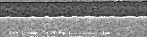
29 Gate Definition: Challenges Must scale to 22 nm Dielectric cap on gate for source/drain regrowth well InP well Metal & Dielectric etch must stop in 5 nm channel Semiconductor etch must not etch through 5 nm InP subchannel Process must leave surfaces ready for S/D regrowth


30 Gate Stack: Multiple Layers & Selective Etches Key: stop etch before reaching dielectric, then gentle low-power etch to stop on dielectric
31 Sidewall Formation well well well (starting material) PECVD Si3N4 ICP RIE etch PECVD SiN sidewall deposition, CF 4 / O 2 low power anisotropic RIE etch...sidewall etch must not damage the channel
32 Clean, Undamaged Surface Before Regrowth undamaged InP subchannel (after Al 2 O 3 dielectric etch & InGaAs recess etch )
33 Two Source/Drain Regrowth Processes non-selective area S/D regrowth by Molecular Beam Epitaxy: Wistey InGaAs well InP well well well well well InP well InP well InP well InP well well InP well (starting material) recess etch nonselective regrowth in-situ S/D metal planarize etch strip planarization material electroplate S/D metal selective area S/D regrowth by Chemical Beam Epitaxy: Palmstrøm / Arkun well well InGaAs well InP well InP well InP well well InP well well InP well well InP well (starting material) CBE in-situ etch CBE selective-area regrowth in-situ S/D metal deposition planarize & etch electroplate S/D metal
34 Recess Etch & Regrowth: Inter-Relationships non-selective regrowth selective CBE regrowth InGaAs well InP well well InP well or well InP well well InP well InGaAs/InP composite channel permits selective InGaAs wet-etch, stopping on InP regrowth initiated iti t on InP (desirable?) If regrowth can extend laterally under sidewall, sidewall can be thicker
35 Regrowth interface resistance In addition to the contact & link resistances source contact metal gate sidewall gate dielectric i drain contact N+ source N+ drain InGaAs channel InP sub-channel substrate resistance at the regrowth interfaces is also of concern...
36 Contact & Regrowth Interface Resistance Selective -Arkun Nonselective -Wistey Mo contact N+ RG N+ InGaAs Mo contact well InP well well InP well Re esistance (Ω) SI InP 0.8 Ω - μm TLM B 2 Mo contact 0.5 Ω - μm TLM A N+ RG N+ InGaAs SI InP 2 Mo contact Pad Spacing (μm)


37 TEM of Regrowth: InGaAs on InGaAs (Mark Wistey) InGaAs n+ regrowth HRTEM Interface HAADF-STEM` InGaAs n+ Interface 2 nm
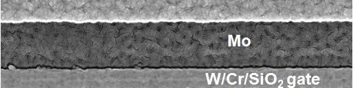
38 Images of MBE Regrowth (dummy sample) Regrowth process is still being de-bugged growth on sidewall: bad! to suppress, grow hotter lateral regrowth under gate: good! Oxide TiW


39 Planarization / Etch-Back Process Ashed-back PR covers S/D contacts Mo etched in SF 6 /Ar dry etch PR strip removes polymers. Mo protects semiconductor from descum plasma.

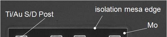
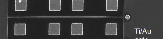
40 Images of Completed Device
 MBE S/D regrowth incomplete S/D growth")


41 Results & Status 1 st working devices: (ISCS submission) MBE S/D regrowth incomplete S/D growth under gate high access resistance low drive current (1 μa/μm!) Cause of Problems related to regrowth on InP subchannel has impacted both MBE & CBE regrowth...and is now resolved New devices now in fabrication...stay tuned
42 InGaAs/InP Channel MOSFETs for VLSI Low-m* materials are beneficial only if EOT cannot scale below ~1/2 nm Devices cannot scale much below 22 nm Lg limits IC density Little CV/I benefit in gate lengths below 22 nm Lg Need device structure with very low access resistance radical re-work of device structure & process flow Gate dielectrics, III-V growth on Si: also under intensive development
Technology Development for InGaAs/InP-channel MOSFETs
 MRS Spring Symposium, Tutorial: Advanced CMOS Substrates, Devices, Reliability, and Characterization, April 13, 2009, San Francisco Technology Development for InGaAs/InP-channel MOSFETs Mark Rodwell University
III-V CMOS: What have we learned from HEMTs? J. A. del Alamo, D.-H. Kim 1, T.-W. Kim, D. Jin, and D. A. Antoniadis
 III-V CMOS: What have we learned from HEMTs? J. A. del Alamo, D.-H. Kim 1, T.-W. Kim, D. Jin, and D. A. Antoniadis Microsystems Technology Laboratories, MIT 1 presently with Teledyne Scientific 23rd International
Quantum-size effects in sub-10 nm fin width InGaAs finfets
 Quantum-size effects in sub-10 nm fin width InGaAs finfets Alon Vardi, Xin Zhao, and Jesús A. del Alamo Microsystems Technology Laboratories, MIT December 9, 2015 Sponsors: DTRA NSF (E3S STC) Northrop
Comparison of Ultra-Thin InAs and InGaAs Quantum Wells and Ultra-Thin-Body Surface-Channel MOSFETs
 Comparison of Ultra-Thin InAs and InGaAs Quantum Wells and Ultra-Thin-Body Surface-Channel MOSFETs Cheng-Ying Huang 1, Sanghoon Lee 1, Evan Wilson 3, Pengyu Long 3, Michael Povolotskyi 3, Varistha Chobpattana
Scaling Issues in Planar FET: Dual Gate FET and FinFETs
 Scaling Issues in Planar FET: Dual Gate FET and FinFETs Lecture 12 Dr. Amr Bayoumi Fall 2014 Advanced Devices (EC760) Arab Academy for Science and Technology - Cairo 1 Outline Scaling Issues for Planar
Self-Aligned InGaAs FinFETs with 5-nm Fin-Width and 5-nm Gate-Contact Separation
 Self-Aligned InGaAs FinFETs with 5-nm Fin-Width and 5-nm Gate-Contact Separation Alon Vardi, Lisa Kong, Wenjie Lu, Xiaowei Cai, Xin Zhao, Jesús Grajal* and Jesús A. del Alamo Microsystems Technology Laboratories,
MOSFET: Introduction
 E&CE 437 Integrated VLSI Systems MOS Transistor 1 of 30 MOSFET: Introduction Metal oxide semiconductor field effect transistor (MOSFET) or MOS is widely used for implementing digital designs Its major
The Prospects for III-Vs
 10 nm CMOS: The Prospects for III-Vs J. A. del Alamo, Dae-Hyun Kim 1, Donghyun Jin, and Taewoo Kim Microsystems Technology Laboratories, MIT 1 Presently with Teledyne Scientific 2010 European Materials
EE410 vs. Advanced CMOS Structures
 EE410 vs. Advanced CMOS Structures Prof. Krishna S Department of Electrical Engineering S 1 EE410 CMOS Structure P + poly-si N + poly-si Al/Si alloy LPCVD PSG P + P + N + N + PMOS N-substrate NMOS P-well
The Pennsylvania State University. Kurt J. Lesker Company. North Carolina State University. Taiwan Semiconductor Manufacturing Company 1
 Enhancement Mode Strained (1.3%) Germanium Quantum Well FinFET (W fin =20nm) with High Mobility (μ Hole =700 cm 2 /Vs), Low EOT (~0.7nm) on Bulk Silicon Substrate A. Agrawal 1, M. Barth 1, G. B. Rayner
EECS130 Integrated Circuit Devices
 EECS130 Integrated Circuit Devices Professor Ali Javey 10/30/2007 MOSFETs Lecture 4 Reading: Chapter 17, 19 Announcements The next HW set is due on Thursday. Midterm 2 is next week!!!! Threshold and Subthreshold
ESE 570: Digital Integrated Circuits and VLSI Fundamentals
 ESE 570: Digital Integrated Circuits and VLSI Fundamentals Lec 4: January 23, 2018 MOS Transistor Theory, MOS Model Penn ESE 570 Spring 2018 Khanna Lecture Outline! CMOS Process Enhancements! Semiconductor
CHAPTER 5 EFFECT OF GATE ELECTRODE WORK FUNCTION VARIATION ON DC AND AC PARAMETERS IN CONVENTIONAL AND JUNCTIONLESS FINFETS
 98 CHAPTER 5 EFFECT OF GATE ELECTRODE WORK FUNCTION VARIATION ON DC AND AC PARAMETERS IN CONVENTIONAL AND JUNCTIONLESS FINFETS In this chapter, the effect of gate electrode work function variation on DC
EE115C Winter 2017 Digital Electronic Circuits. Lecture 3: MOS RC Model, CMOS Manufacturing
 EE115C Winter 2017 Digital Electronic Circuits Lecture 3: MOS RC Model, CMOS Manufacturing Agenda MOS Transistor: RC Model (pp. 104-113) S R on D CMOS Manufacturing Process (pp. 36-46) S S C GS G G C GD
Performance Analysis of Ultra-Scaled InAs HEMTs
 Purdue University Purdue e-pubs Birck and NCN Publications Birck Nanotechnology Center 2009 Performance Analysis of Ultra-Scaled InAs HEMTs Neerav Kharche Birck Nanotechnology Center and Purdue University,
Chapter 5 MOSFET Theory for Submicron Technology
 Chapter 5 MOSFET Theory for Submicron Technology Short channel effects Other small geometry effects Parasitic components Velocity saturation/overshoot Hot carrier effects ** Majority of these notes are
S=0.7 [0.5x per 2 nodes] ESE370: Circuit-Level Modeling, Design, and Optimization for Digital Systems. Today. Scaling ITRS Roadmap
![S=0.7 [0.5x per 2 nodes] ESE370: Circuit-Level Modeling, Design, and Optimization for Digital Systems. Today. Scaling ITRS Roadmap](/thumbs/92/110446830.jpg "S=0.7 [0.5x per 2 nodes] ESE370: Circuit-Level Modeling, Design, and Optimization for Digital Systems. Today. Scaling ITRS Roadmap") ESE370: Circuit-Level Modeling, Design, and Optimization for Digital Systems Day 15: October 4, 2013 Scaling Today VLSI Scaling Trends/Disciplines Effects Alternatives (cheating) 1 2 Scaling ITRS Roadmap
ESE370: Circuit-Level Modeling, Design, and Optimization for Digital Systems Day 15: October 4, 2013 Scaling Today VLSI Scaling Trends/Disciplines Effects Alternatives (cheating) 1 2 Scaling ITRS Roadmap
CMPEN 411 VLSI Digital Circuits. Lecture 03: MOS Transistor
 CMPEN 411 VLSI Digital Circuits Lecture 03: MOS Transistor Kyusun Choi [Adapted from Rabaey s Digital Integrated Circuits, Second Edition, 2003 J. Rabaey, A. Chandrakasan, B. Nikolic] CMPEN 411 L03 S.1
High aspect-ratio InGaAs FinFETs with sub-20 nm fin width
 High aspect-rati InGaAs FinFETs with sub-2 nm fin width Aln Vardi, Jianqiang Lin, Wenjie Lu, Xin Zha and Jesús A. del Alam Micrsystems Technlgy Labratries, MIT June 15, 216 Spnsrs: DTRA (HDTRA 1-14-1-57),
Performance Analysis of 60-nm Gate-Length III-V InGaAs HEMTs: Simulations Versus Experiments
 Purdue University Purdue e-pubs Birck and NCN Publications Birck Nanotechnology Center 7-2009 Performance Analysis of 60-nm Gate-Length III-V InGaAs HEMTs: Simulations Versus Experiments Neophytou Neophytos
MOS Transistor Properties Review
 MOS Transistor Properties Review 1 VLSI Chip Manufacturing Process Photolithography: transfer of mask patterns to the chip Diffusion or ion implantation: selective doping of Si substrate Oxidation: SiO
The Devices. Devices
 The The MOS Transistor Gate Oxyde Gate Source n+ Polysilicon Drain n+ Field-Oxyde (SiO 2 ) p-substrate p+ stopper Bulk Contact CROSS-SECTION of NMOS Transistor Cross-Section of CMOS Technology MOS transistors
InGaAs Double-Gate Fin-Sidewall MOSFET
 InGaAs Double-Gate Fin-Sidewall MOSFET Alon Vardi, Xin Zhao and Jesús del Alamo Microsystems Technology Laboratories, MIT June 25, 214 Sponsors: Sematech, Technion-MIT Fellowship, and NSF E3S Center (#939514)
Lecture 6: 2D FET Electrostatics
 Lecture 6: 2D FET Electrostatics 2016-02-01 Lecture 6, High Speed Devices 2014 1 Lecture 6: III-V FET DC I - MESFETs Reading Guide: Liu: 323-337 (he mainly focuses on the single heterostructure FET) Jena:
Ultra-Scaled InAs HEMTs
 Performance Analysis of Ultra-Scaled InAs HEMTs Neerav Kharche 1, Gerhard Klimeck 1, Dae-Hyun Kim 2,3, Jesús. A. del Alamo 2, and Mathieu Luisier 1 1 Network for Computational ti Nanotechnology and Birck
Lecture #27. The Short Channel Effect (SCE)
") Lecture #27 ANNOUNCEMENTS Design Project: Your BJT design should meet the performance specifications to within 10% at both 300K and 360K. ( β dc > 45, f T > 18 GHz, V A > 9 V and V punchthrough > 9 V )
Lecture #27 ANNOUNCEMENTS Design Project: Your BJT design should meet the performance specifications to within 10% at both 300K and 360K. ( β dc > 45, f T > 18 GHz, V A > 9 V and V punchthrough > 9 V )
Scaling of MOS Circuits. 4. International Technology Roadmap for Semiconductors (ITRS) 6. Scaling factors for device parameters
 6. Scaling factors for device parameters") 1 Scaling of MOS Circuits CONTENTS 1. What is scaling?. Why scaling? 3. Figure(s) of Merit (FoM) for scaling 4. International Technology Roadmap for Semiconductors (ITRS) 5. Scaling models 6. Scaling factors
1 Scaling of MOS Circuits CONTENTS 1. What is scaling?. Why scaling? 3. Figure(s) of Merit (FoM) for scaling 4. International Technology Roadmap for Semiconductors (ITRS) 5. Scaling models 6. Scaling factors
ESE 570: Digital Integrated Circuits and VLSI Fundamentals
 ESE 570: Digital Integrated Circuits and VLSI Fundamentals Lec 4: January 29, 2019 MOS Transistor Theory, MOS Model Penn ESE 570 Spring 2019 Khanna Lecture Outline! CMOS Process Enhancements! Semiconductor
Lecture 5: CMOS Transistor Theory
 Lecture 5: CMOS Transistor Theory Slides courtesy of Deming Chen Slides based on the initial set from David Harris CMOS VLSI Design Outline q q q q q q q Introduction MOS Capacitor nmos I-V Characteristics
Microsystems Technology Laboratories, MIT. Teledyne Scientific Company (TSC)
") Extraction of Virtual-Source Injection Velocity in sub-100 nm III-V HFETs 1,2) D.-H. Kim, 1) J. A. del Alamo, 1) D. A. Antoniadis and 2) B. Brar 1) Microsystems Technology Laboratories, MIT 2) Teledyne
Extraction of Virtual-Source Injection Velocity in sub-100 nm III-V HFETs 1,2) D.-H. Kim, 1) J. A. del Alamo, 1) D. A. Antoniadis and 2) B. Brar 1) Microsystems Technology Laboratories, MIT 2) Teledyne
! CMOS Process Enhancements. ! Semiconductor Physics. " Band gaps. " Field Effects. ! MOS Physics. " Cut-off. " Depletion.
 ESE 570: Digital Integrated Circuits and VLSI Fundamentals Lec 4: January 3, 018 MOS Transistor Theory, MOS Model Lecture Outline! CMOS Process Enhancements! Semiconductor Physics " Band gaps " Field Effects!
Long Channel MOS Transistors
 Long Channel MOS Transistors The theory developed for MOS capacitor (HO #2) can be directly extended to Metal-Oxide-Semiconductor Field-Effect transistors (MOSFET) by considering the following structure:
Performance Enhancement of P-channel InGaAs Quantum-well FETs by Superposition of Process-induced Uniaxial Strain and Epitaxially-grown Biaxial Strain
 Performance Enhancement of P-channel InGaAs Quantum-well FETs by Superposition of Process-induced Uniaxial Strain and Epitaxially-grown Biaxial Strain Ling Xia 1, Vadim Tokranov 2, Serge R. Oktyabrsky
MOS Transistor Theory
 CHAPTER 3 MOS Transistor Theory Outline 2 1. Introduction 2. Ideal I-V Characteristics 3. Nonideal I-V Effects 4. C-V Characteristics 5. DC Transfer Characteristics 6. Switch-level RC Delay Models MOS
MOS Transistor I-V Characteristics and Parasitics
 ECEN454 Digital Integrated Circuit Design MOS Transistor I-V Characteristics and Parasitics ECEN 454 Facts about Transistors So far, we have treated transistors as ideal switches An ON transistor passes
Components Research, TMG Intel Corporation *QinetiQ. Contact:
 1 High-Performance 4nm Gate Length InSb P-Channel Compressively Strained Quantum Well Field Effect Transistors for Low-Power (V CC =.5V) Logic Applications M. Radosavljevic,, T. Ashley*, A. Andreev*, S.
THz Bipolar Transistor Circuits: Technical Feasibility, Technology Development, Integrated Circuit Results
 Plenary, 2008 IEEE-SI Symposium, October 12, 2008 THz Bipolar Transistor ircuits: Technical Feasibility, Technology Development, Integrated ircuit Results Mark Rodwell University of alifornia, Santa Barbara
VLSI Design and Simulation
 VLSI Design and Simulation Performance Characterization Topics Performance Characterization Resistance Estimation Capacitance Estimation Inductance Estimation Performance Characterization Inverter Voltage
Lecture 12: MOS Capacitors, transistors. Context
 Lecture 12: MOS Capacitors, transistors Context In the last lecture, we discussed PN diodes, and the depletion layer into semiconductor surfaces. Small signal models In this lecture, we will apply those
30 nm In 0.7 Ga 0.3 As Inverted-type HEMT with Reduced Gate Leakage Current for Logic Applications
 30 nm In 0.7 Ga 0.3 As Inverted-type HEMT with Reduced Gate Leakage Current for Logic Applications T.-W. Kim, D.-H. Kim* and J. A. del Alamo Microsystems Technology Laboratories MIT Presently with Teledyne
MOS Transistors. Prof. Krishna Saraswat. Department of Electrical Engineering Stanford University Stanford, CA
 MOS Transistors Prof. Krishna Saraswat Department of Electrical Engineering S Stanford, CA 94305 saraswat@stanford.edu 1 1930: Patent on the Field-Effect Transistor! Julius Lilienfeld filed a patent describing
Low Frequency Noise in MoS 2 Negative Capacitance Field-effect Transistor
 Low Frequency Noise in MoS Negative Capacitance Field-effect Transistor Sami Alghamdi, Mengwei Si, Lingming Yang, and Peide D. Ye* School of Electrical and Computer Engineering Purdue University West Lafayette,
Supporting Online Material for
 www.sciencemag.org/cgi/content/full/327/5966/662/dc Supporting Online Material for 00-GHz Transistors from Wafer-Scale Epitaxial Graphene Y.-M. Lin,* C. Dimitrakopoulos, K. A. Jenkins, D. B. Farmer, H.-Y.
Lecture 4: CMOS Transistor Theory
 Introduction to CMOS VLSI Design Lecture 4: CMOS Transistor Theory David Harris, Harvey Mudd College Kartik Mohanram and Steven Levitan University of Pittsburgh Outline q Introduction q MOS Capacitor q
Stretching the Barriers An analysis of MOSFET Scaling. Presenters (in order) Zeinab Mousavi Stephanie Teich-McGoldrick Aseem Jain Jaspreet Wadhwa
 Zeinab Mousavi Stephanie Teich-McGoldrick Aseem Jain Jaspreet Wadhwa") Stretching the Barriers An analysis of MOSFET Scaling Presenters (in order) Zeinab Mousavi Stephanie Teich-McGoldrick Aseem Jain Jaspreet Wadhwa Why Small? Higher Current Lower Gate Capacitance Higher
Stretching the Barriers An analysis of MOSFET Scaling Presenters (in order) Zeinab Mousavi Stephanie Teich-McGoldrick Aseem Jain Jaspreet Wadhwa Why Small? Higher Current Lower Gate Capacitance Higher
EEC 118 Lecture #2: MOSFET Structure and Basic Operation. Rajeevan Amirtharajah University of California, Davis Jeff Parkhurst Intel Corporation
 EEC 118 Lecture #2: MOSFET Structure and Basic Operation Rajeevan Amirtharajah University of California, Davis Jeff Parkhurst Intel Corporation Announcements Lab 1 this week, report due next week Bring
! CMOS Process Enhancements. ! Semiconductor Physics. " Band gaps. " Field Effects. ! MOS Physics. " Cut-off. " Depletion.
 ESE 570: Digital Integrated Circuits and VLSI Fundamentals Lec 4: January 9, 019 MOS Transistor Theory, MOS Model Lecture Outline CMOS Process Enhancements Semiconductor Physics Band gaps Field Effects
LECTURE 3 MOSFETS II. MOS SCALING What is Scaling?
 LECTURE 3 MOSFETS II Lecture 3 Goals* * Understand constant field and constant voltage scaling and their effects. Understand small geometry effects for MOS transistors and their implications modeling and
High Mobility Materials and Novel Device Structures for High Performance Nanoscale MOSFETs
 High Mobility Materials and Novel Device Structures for High Performance Nanoscale MOSFETs Prof. (Dr.) Tejas Krishnamohan Department of Electrical Engineering Stanford University, CA & Intel Corporation
Metal-oxide-semiconductor field effect transistors (2 lectures)
") Metal-ide-semiconductor field effect transistors ( lectures) MOS physics (brief in book) Current-voltage characteristics - pinch-off / channel length modulation - weak inversion - velocity saturation -
Metal-ide-semiconductor field effect transistors ( lectures) MOS physics (brief in book) Current-voltage characteristics - pinch-off / channel length modulation - weak inversion - velocity saturation -
A final review session will be offered on Thursday, May 10 from 10AM to 12noon in 521 Cory (the Hogan Room).
.") A final review session will be offered on Thursday, May 10 from 10AM to 12noon in 521 Cory (the Hogan Room). The Final Exam will take place from 12:30PM to 3:30PM on Saturday May 12 in 60 Evans.» All of
A final review session will be offered on Thursday, May 10 from 10AM to 12noon in 521 Cory (the Hogan Room). The Final Exam will take place from 12:30PM to 3:30PM on Saturday May 12 in 60 Evans.» All of
The Devices. Digital Integrated Circuits A Design Perspective. Jan M. Rabaey Anantha Chandrakasan Borivoje Nikolic. July 30, 2002
 Digital Integrated Circuits A Design Perspective Jan M. Rabaey Anantha Chandrakasan Borivoje Nikolic The Devices July 30, 2002 Goal of this chapter Present intuitive understanding of device operation Introduction
Fabrication Technology, Part I
 EEL5225: Principles of MEMS Transducers (Fall 2004) Fabrication Technology, Part I Agenda: Microfabrication Overview Basic semiconductor devices Materials Key processes Oxidation Thin-film Deposition Reading:
Multiple Gate CMOS and Beyond
 Multiple CMOS and Beyond Dept. of EECS, KAIST Yang-Kyu Choi Outline 1. Ultimate Scaling of MOSFETs - 3nm Nanowire FET - 8nm Non-Volatile Memory Device 2. Multiple Functions of MOSFETs 3. Summary 2 CMOS
L ECE 4211 UConn F. Jain Scaling Laws for NanoFETs Chapter 10 Logic Gate Scaling
 L13 04202017 ECE 4211 UConn F. Jain Scaling Laws for NanoFETs Chapter 10 Logic Gate Scaling Scaling laws: Generalized scaling (GS) p. 610 Design steps p.613 Nanotransistor issues (page 626) Degradation
Enhanced Mobility CMOS
 Enhanced Mobility CMOS Judy L. Hoyt I. Åberg, C. Ni Chléirigh, O. Olubuyide, J. Jung, S. Yu, E.A. Fitzgerald, and D.A. Antoniadis Microsystems Technology Laboratory MIT, Cambridge, MA 02139 Acknowledge
Lecture 8: Ballistic FET I-V
 Lecture 8: Ballistic FET I-V 1 Lecture 1: Ballistic FETs Jena: 61-70 Diffusive Field Effect Transistor Source Gate L g >> l Drain Source V GS Gate Drain I D Mean free path much shorter than channel length
The Devices. Digital Integrated Circuits A Design Perspective. Jan M. Rabaey Anantha Chandrakasan Borivoje Nikolic. July 30, 2002
 igital Integrated Circuits A esign Perspective Jan M. Rabaey Anantha Chandrakasan Borivoje Nikolic The evices July 30, 2002 Goal of this chapter Present intuitive understanding of device operation Introduction
A Multi-Gate CMOS Compact Model BSIMMG
 A Multi-Gate CMOS Compact Model BSIMMG Darsen Lu, Sriramkumar Venugopalan, Tanvir Morshed, Yogesh Singh Chauhan, Chung-Hsun Lin, Mohan Dunga, Ali Niknejad and Chenming Hu University of California, Berkeley
Lecture 3: Transistor as an thermonic switch
 Lecture 3: Transistor as an thermonic switch 2016-01-21 Lecture 3, High Speed Devices 2016 1 Lecture 3: Transistors as an thermionic switch Reading Guide: 54-57 in Jena Transistor metrics Reservoir equilibrium
The Devices: MOS Transistors
 The Devices: MOS Transistors References: Semiconductor Device Fundamentals, R. F. Pierret, Addison-Wesley Digital Integrated Circuits: A Design Perspective, J. Rabaey et.al. Prentice Hall NMOS Transistor
Final Examination EE 130 December 16, 1997 Time allotted: 180 minutes
 Final Examination EE 130 December 16, 1997 Time allotted: 180 minutes Problem 1: Semiconductor Fundamentals [30 points] A uniformly doped silicon sample of length 100µm and cross-sectional area 100µm 2
Ion Implantation. alternative to diffusion for the introduction of dopants essentially a physical process, rather than chemical advantages:
 Ion Implantation alternative to diffusion for the introduction of dopants essentially a physical process, rather than chemical advantages: mass separation allows wide varies of dopants dose control: diffusion
! MOS Capacitances. " Extrinsic. " Intrinsic. ! Lumped Capacitance Model. ! First Order Capacitor Summary. ! Capacitance Implications
 ESE 570: Digital Integrated Circuits and VLSI Fundamentals Lec 7: February, 07 MOS SPICE Models, MOS Parasitic Details Lecture Outline! MOS Capacitances " Extrinsic " Intrinsic! Lumped Capacitance Model!
VLSI Design The MOS Transistor
 VLSI Design The MOS Transistor Frank Sill Torres Universidade Federal de Minas Gerais (UFMG), Brazil VLSI Design: CMOS Technology 1 Outline Introduction MOS Capacitor nmos I-V Characteristics pmos I-V
Simple and accurate modeling of the 3D structural variations in FinFETs
 Simple and accurate modeling of the 3D structural variations in FinFETs Donghu Kim Electrical Engineering Program Graduate school of UNIST 2013 Simple and accurate modeling of the 3D structural variations
ECE 305 Exam 5 SOLUTIONS: Spring 2015 April 17, 2015 Mark Lundstrom Purdue University
 NAME: PUID: : ECE 305 Exam 5 SOLUTIONS: April 17, 2015 Mark Lundstrom Purdue University This is a closed book exam. You may use a calculator and the formula sheet at the end of this exam. Following the
GaN based transistors
 GaN based transistors S FP FP dielectric G SiO 2 Al x Ga 1-x N barrier i-gan Buffer i-sic D Transistors "The Transistor was probably the most important invention of the 20th Century The American Institute
Subthreshold and scaling of PtSi Schottky barrier MOSFETs
 Superlattices and Microstructures, Vol. 28, No. 5/6, 2000 doi:10.1006/spmi.2000.0954 Available online at http://www.idealibrary.com on Subthreshold and scaling of PtSi Schottky barrier MOSFETs L. E. CALVET,
Journal of Electron Devices, Vol. 18, 2013, pp JED [ISSN: ]
![Journal of Electron Devices, Vol. 18, 2013, pp JED [ISSN: ]](/thumbs/86/93990983.jpg "Journal of Electron Devices, Vol. 18, 2013, pp JED [ISSN: ]") DrainCurrent-Id in linearscale(a/um) Id in logscale Journal of Electron Devices, Vol. 18, 2013, pp. 1582-1586 JED [ISSN: 1682-3427 ] SUITABILITY OF HIGH-k GATE DIELECTRICS ON THE DEVICE PERFORMANCE AND
DrainCurrent-Id in linearscale(a/um) Id in logscale Journal of Electron Devices, Vol. 18, 2013, pp. 1582-1586 JED [ISSN: 1682-3427 ] SUITABILITY OF HIGH-k GATE DIELECTRICS ON THE DEVICE PERFORMANCE AND
The Future of CMOS. David Pulfrey. CHRONOLOGY of the FET. Lecture Lilienfeld s patent (BG FET) 1965 Commercialization (Fairchild)
 1965 Commercialization (Fairchild)") The Future of CMOS David Pulfrey 1 CHRONOLOGY of the FET 1933 Lilienfeld s patent (BG FET) 1965 Commercialization (Fairchild) 1991 The most abundant object made by mankind (C.T. Sah) 2003 The 10 nm FET
The Future of CMOS David Pulfrey 1 CHRONOLOGY of the FET 1933 Lilienfeld s patent (BG FET) 1965 Commercialization (Fairchild) 1991 The most abundant object made by mankind (C.T. Sah) 2003 The 10 nm FET
Recent Development of FinFET Technology for CMOS Logic and Memory
 Recent Development of FinFET Technology for CMOS Logic and Memory Chung-Hsun Lin EECS Department University of California at Berkeley Why FinFET Outline FinFET process Unique features of FinFET Mobility,
ECE 497 JS Lecture - 12 Device Technologies
 ECE 497 JS Lecture - 12 Device Technologies Spring 2004 Jose E. Schutt-Aine Electrical & Computer Engineering University of Illinois jose@emlab.uiuc.edu 1 NMOS Transistor 2 ρ Source channel charge density
EE 560 MOS TRANSISTOR THEORY PART 2. Kenneth R. Laker, University of Pennsylvania
 1 EE 560 MOS TRANSISTOR THEORY PART nmos TRANSISTOR IN LINEAR REGION V S = 0 V G > V T0 channel SiO V D = small 4 C GC C BC substrate depletion region or bulk B p nmos TRANSISTOR AT EDGE OF SATURATION
P. R. Nelson 1 ECE418 - VLSI. Midterm Exam. Solutions
 P. R. Nelson 1 ECE418 - VLSI Midterm Exam Solutions 1. (8 points) Draw the cross-section view for A-A. The cross-section view is as shown below.. ( points) Can you tell which of the metal1 regions is the
Self-study problems and questions Processing and Device Technology, FFF110/FYSD13
 Self-study problems and questions Processing and Device Technology, FFF110/FYSD13 Version 2016_01 In addition to the problems discussed at the seminars and at the lectures, you can use this set of problems
SECTION: Circle one: Alam Lundstrom. ECE 305 Exam 5 SOLUTIONS: Spring 2016 April 18, 2016 M. A. Alam and M.S. Lundstrom Purdue University
 NAME: PUID: SECTION: Circle one: Alam Lundstrom ECE 305 Exam 5 SOLUTIONS: April 18, 2016 M A Alam and MS Lundstrom Purdue University This is a closed book exam You may use a calculator and the formula
Quantum Mechanical Simulation for Ultra-thin High-k Gate Dielectrics Metal Oxide Semiconductor Field Effect Transistors
 Mechanical Simulation for Ultra-thin High-k Gate Dielectrics Metal Oxide Semiconductor Field Effect Transistors Shih-Ching Lo 1, Yiming Li 2,3, and Jyun-Hwei Tsai 1 1 National Center for High-Performance
Prospects for Ge MOSFETs
 Prospects for Ge MOSFETs Sematech Workshop December 4, 2005 Dimitri A. Antoniadis Microsystems Technology Laboratories MIT Sematech Workshop 2005 1 Channel Transport - I D I D =WQ i (x 0 )v xo v xo : carrier
ELEN0037 Microelectronic IC Design. Prof. Dr. Michael Kraft
 ELEN0037 Microelectronic IC Design Prof. Dr. Michael Kraft Lecture 2: Technological Aspects Technology Passive components Active components CMOS Process Basic Layout Scaling CMOS Technology Integrated
ECE 342 Electronic Circuits. Lecture 6 MOS Transistors
 ECE 342 Electronic Circuits Lecture 6 MOS Transistors Jose E. Schutt-Aine Electrical & Computer Engineering University of Illinois jesa@illinois.edu 1 NMOS Transistor Typically L = 0.1 to 3 m, W = 0.2
Fundamentals of the Metal Oxide Semiconductor Field-Effect Transistor
 Triode Working FET Fundamentals of the Metal Oxide Semiconductor Field-Effect Transistor The characteristics of energy bands as a function of applied voltage. Surface inversion. The expression for the
Introduction to CMOS VLSI. Chapter 2: CMOS Transistor Theory. Harris, 2004 Updated by Li Chen, Outline
 Introduction to MOS VLSI Design hapter : MOS Transistor Theory copyright@david Harris, 004 Updated by Li hen, 010 Outline Introduction MOS apacitor nmos IV haracteristics pmos IV haracteristics Gate and
Lecture 3: CMOS Transistor Theory
 Lecture 3: CMOS Transistor Theory Outline Introduction MOS Capacitor nmos I-V Characteristics pmos I-V Characteristics Gate and Diffusion Capacitance 2 Introduction So far, we have treated transistors
ECE-305: Fall 2017 MOS Capacitors and Transistors
 ECE-305: Fall 2017 MOS Capacitors and Transistors Pierret, Semiconductor Device Fundamentals (SDF) Chapters 15+16 (pp. 525-530, 563-599) Professor Peter Bermel Electrical and Computer Engineering Purdue
Normally-Off GaN Field Effect Power Transistors: Device Design and Process Technology Development
 Center for High Performance Power Electronics Normally-Off GaN Field Effect Power Transistors: Device Design and Process Technology Development Dr. Wu Lu (614-292-3462, lu.173@osu.edu) Dr. Siddharth Rajan
ECE 342 Electronic Circuits. 3. MOS Transistors
 ECE 342 Electronic Circuits 3. MOS Transistors Jose E. Schutt-Aine Electrical & Computer Engineering University of Illinois jschutt@emlab.uiuc.edu 1 NMOS Transistor Typically L = 0.1 to 3 m, W = 0.2 to
JFET/MESFET. JFET: small gate current (reverse leakage of the gate-to-channel junction) More gate leakage than MOSFET, less than bipolar.
 More gate leakage than MOSFET, less than bipolar.") JFET/MESFET JFET: small gate current (reverse leakage of the gate-to-channel junction) More gate leakage than MOSFET, less than bipolar. JFET has higher transconductance than the MOSFET. Used in low-noise,
JFET/MESFET JFET: small gate current (reverse leakage of the gate-to-channel junction) More gate leakage than MOSFET, less than bipolar. JFET has higher transconductance than the MOSFET. Used in low-noise,
Microelectronics Part 1: Main CMOS circuits design rules
 GBM8320 Dispositifs Médicaux telligents Microelectronics Part 1: Main CMOS circuits design rules Mohamad Sawan et al. Laboratoire de neurotechnologies Polystim! http://www.cours.polymtl.ca/gbm8320/! med-amine.miled@polymtl.ca!
ESE534: Computer Organization. Today. Why Care? Why Care. Scaling. Preclass
 ESE534: Computer Organization Today Day 7: February 8, 2010 VLSI Scaling VLSI Scaling Rules Effects Historical/predicted scaling Variations (cheating) Limits 1 2 Why Care? In this game, we must be able
MOS Transistor Theory MOSFET Symbols Current Characteristics of MOSFET. MOS Symbols and Characteristics. nmos Enhancement Transistor
 MOS Transistor Theory MOSFET Symbols Current Characteristics of MOSFET Calculation of t and Important 2 nd Order Effects SmallSignal Signal MOSFET Model Summary Material from: CMOS LSI Design By Weste
Metallic: 2n 1. +n 2. =3q Armchair structure always metallic = 2
 Properties of CNT d = 2.46 n 2 2 1 + n1n2 + n2 2π Metallic: 2n 1 +n 2 =3q Armchair structure always metallic a) Graphite Valence(π) and Conduction(π*) states touch at six points(fermi points) Carbon Nanotube:
Introduction and Background
 Analog CMOS Integrated Circuit Design Introduction and Background Dr. Jawdat Abu-Taha Department of Electrical and Computer Engineering Islamic University of Gaza jtaha@iugaza.edu.ps 1 Marking Assignments
Section 12: Intro to Devices
 Section 12: Intro to Devices Extensive reading materials on reserve, including Robert F. Pierret, Semiconductor Device Fundamentals EE143 Ali Javey Bond Model of Electrons and Holes Si Si Si Si Si Si Si
Electric-Field Induced F - Migration in Self-Aligned InGaAs MOSFETs and Mitigation
 Electric-Field Induced F - Migration in Self-Aligned InGaAs MOSFETs and Mitigation X. Cai, J. Lin, D. A. Antoniadis and J. A. del Alamo Microsystems Technology Laboratories, MIT December 5, 2016 Sponsors:
EE5311- Digital IC Design
 EE5311- Digital IC Design Module 1 - The Transistor Janakiraman V Assistant Professor Department of Electrical Engineering Indian Institute of Technology Madras Chennai October 28, 2017 Janakiraman, IITM
FIELD-EFFECT TRANSISTORS
 FIEL-EFFECT TRANSISTORS 1 Semiconductor review 2 The MOS capacitor 2 The enhancement-type N-MOS transistor 3 I-V characteristics of enhancement MOSFETS 4 The output characteristic of the MOSFET in saturation
The Critical Role of Quantum Capacitance in Compact Modeling of Nano-Scaled and Nanoelectronic Devices
 The Critical Role of Quantum Capacitance in Compact Modeling of Nano-Scaled and Nanoelectronic Devices Zhiping Yu and Jinyu Zhang Institute of Microelectronics Tsinghua University, Beijing, China yuzhip@tsinghua.edu.cn
Chapter 4 Field-Effect Transistors
 Chapter 4 Field-Effect Transistors Microelectronic Circuit Design Richard C. Jaeger Travis N. Blalock 5/5/11 Chap 4-1 Chapter Goals Describe operation of MOSFETs. Define FET characteristics in operation
Field effect = Induction of an electronic charge due to an electric field Example: Planar capacitor
 JFETs AND MESFETs Introduction Field effect = Induction of an electronic charge due to an electric field Example: Planar capacitor Why would an FET made of a planar capacitor with two metal plates, as