Fundamentals of Nanoelectronics: Basic Concepts
|
|
|
- Daniel Griffith
- 6 years ago
- Views:
Transcription

1 Fundamentals of Nanoelectronics: Basic Concepts Sławomir Prucnal FWIM Page 1
2 Introduction Outline Electronics in nanoscale Transport Ohms law Optoelectronic properties of semiconductors Optics in nanoscale Band gap Quantum confinement effect Page 2
3 Photolithography Ion implantation Etching Temporary Gate Formation Silicon wafer metalization Page 3
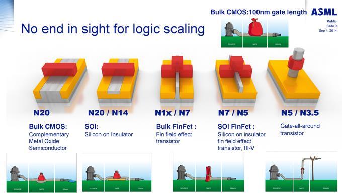
4 Introduction NEAR-TERM Scaling of Si CMOS - Implementation of fully depleted SOI Implementation of high-mobility CMOS channel materials Page 4
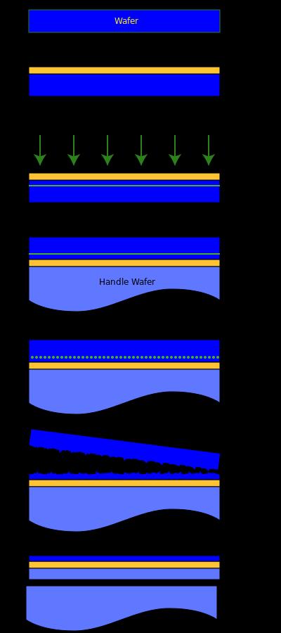
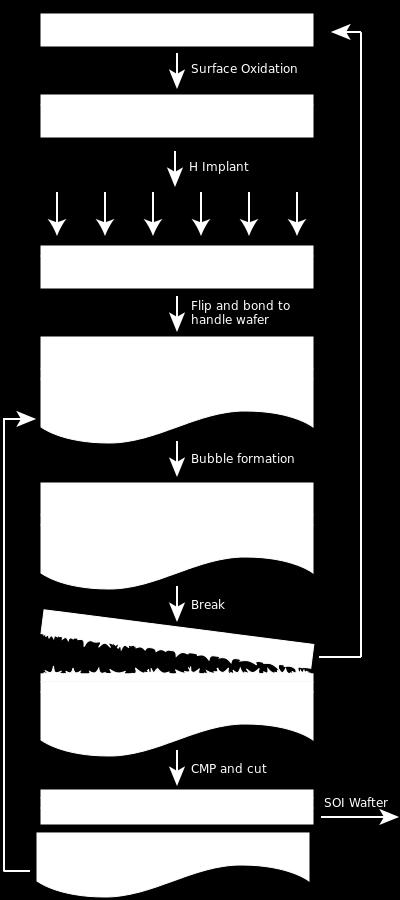
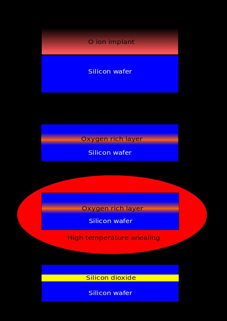


5 SmartCut Introduction SIMOX process SOI Page 5 From Wikipedia


6 Introduction Silicon wafer technique/physical-verification-design-finfet-fd-soi/ &h=532&w=980&tbnid=bg2t-9aazopmjm:&tbnh=90&tbnw=166&usg= 3fSXT57run64yrsHWP2cDxmXjfs=&docid=9ZIFDJ9SQcwv AM&sa=X&ved=0CEAQ9QEwBWoVChMIrqu3kfrAxwIVw7kUCh3DKQn5 (Source: Synopsys) Page 6

7 Introduction technique/physical-verification-design-finfet-fd-soi/ &h=532&w=980&tbnid=bg2t-9aazopmjm:&tbnh=90&tbnw=166&usg= 3fSXT57run64yrsHWP2cDxmXjfs=&docid=9ZIFDJ9SQcwv AM&sa=X&ved=0CEAQ9QEwBWoVChMIrqu3kfrAxwIVw7kUCh3DKQn5 (Source: Synopsys) Page 7
 Faster switching speed Availability of strain engineering Challanges Very restrictive design options Fin width variability and edge")
8 Introduction The main manufacturing challenges for finfets (above 20 nm) are: - controlling the etch along the edges - uniform doping of 3D surfaces - Deposition of all the films used in the gate stack Benefits reduction in power consumption (~50% over 32nm) Faster switching speed Availability of strain engineering Challanges Very restrictive design options Fin width variability and edge quality leads to variability in threshold voltage V T Extra manufacturing complexity and expense Page 8

9 Fully depleted silicon-on-insulator FD-SOI vs PD-SOI The top silicon layer is typically between 50 and 90 nmthick Silicon under the channel is partially depleted of mobile charge carriers. The top silicon layer is between 5 and 20 nm thick, typically ¼ of the gate length Silicon under the gate is fully depleted of mobile charge carriers. There is no floating body effect. Page 9
10 Introduction Fully depleted silicon-on-insulator FD-SOI (below 14 nm) Benefits Significant reduction in power consumption below 11 nm Faster switching speed Easier, standard manufacturing process Challanges High cost of initial wafers Variability in V T due to variations in the thickness of silicon thin-film No strain engineering possible Availability of back-biasing to control V T No doping variability Page 10 10
11 Introduction NEAR-TERM Scaling of Si CMOS - Implementation of fully depleted SOI Implementation of high-mobility CMOS channel materials LONG-TERM Implementation of advanced multi-gate structures ultra-thin body multi-gate MOSFETs Page 11

12 Multi-gate structures jpg%253f blob%253dnormal&imgrefurl=http%3a%2f%2fwww.fz-juelich.de%2fpgi%2fpgi-9%2fde%2fforschung%2f05-si-nano-mosfet%2f01-multigate%2520nanowire%2f_node.html&h= 336&w=600&tbnid=4kA-VMzzxXDUlM%3A&docid=ZqBKi7JKfbji2M&ei=OrjaVbjkF4n0ULaHjdAE&tbm=isch&iact=rc&uact=3&dur=2146&page=1&start=0&ndsp=30&ved=0CHQQrQMw GmoVChMIuOnjrIrBxwIVCToUCh22QwNK Page 12
13 Multi-gate structures Page 13


14 Hybrid 1D and 3D nanostructures Room temperature semi-logarithmic I-V characteristic of n-inas/p-si heterojunction. AFM topography of annealed and etched sample Prucnal et al. Nanolett. 11, 2814, (2011) Page 14

15 Hybrid 1D and 3D nanostructures InAs Page 15

16 Hybrid 1D and 3D nanostructures Page 16


")
17 Current (A) GeOI for junctionless transistors x100x3000 nm H x W x L 100 nm Ge 50 nm Ge x50x3000 nm H x W x L Voltage (V) Page 17
18 Electronic transport Page 18
19 3 cm 300 length scale: transistor density 1 mm = 1m/ mm channel length 1 mm = 1mm/ < 100 nm 2015 < 20 nm 1 nm = 1mm/1000 Atomic distance < 1 nm For the channel length of 10 mm size of transisotr is 100 mm 3 cm Page 19
20 3 cm length scale: transistor density 1 mm = 1m/ mm channel length 1 mm = 1mm/ < 100 nm 2015 < 20 nm 1 nm = 1mm/1000 Atomic distance < 1 nm For the channel length of 100 nm size of transisotr is 1 mm 3 cm Page 20
21 3 cm length scale: transistor density 1 mm = 1m/ mm channel length 1 mm = 1mm/ < 100 nm 2015 < 20 nm 1 nm = 1mm/1000 Atomic distance < 1 nm For the channel length of 20 nm size of transisotr is 200 nm 3 cm Page 21
22 length scale:electronic transport 1 mm = 1m/ mm 1 mm = 1mm/ < 100 nm 2015 < 20 nm 1 nm = 1mm/1000 Atomic distance < 1 nm S V o - + Channel V I =R I D R determines On/Off state and is controlled by 3 rd terminal Page 22
23 length scale:electronic transport 1 mm = 1m/ mm 1 mm = 1mm/ < 100 nm 2015 < 20 nm 1 nm = 1mm/1000 Atomic distance < 1 nm S e V o - + Channel I e D Diffusive transport Page 23

24 length scale:electronic transport 1 mm = 1m/ mm 1 mm = 1mm/ < 100 nm 2015 < 20 nm 1 nm = 1mm/1000 Atomic distance < 1 nm S e V o - + Channel I e D Ballistic transport Page 24
25 length scale: Ohms law S ~mm ~nm V o Channel D S V - + V =R I I W V - V o Channel L + I =R= ρ W L I D I =R= ρ W (L + m eanf ree p ath ) R=r L A, L 0, R 0, R = h q 2=25kW for ballistic transport Page 25
26 length scale: Ohms law G. Jo et al. J. Appl. Phys. 102, (2007) Page 26
27 Mobility Page 27
28 length scale: mobility Page 28
29 length scale: mobility Ballistic transport Diffusive transport F Gámiz 2004 Semicond. Sci. Technol Page 29
30 length scale: mobility Patrick S. Goley * and Mantu K. Hudait Materials 2014, 7(3), Page 30
31 Mobility cm 2 /Vs Mobility cm 2 /Vs GeOI for junctionless transistors SmartCut GeOI Epi-Ge University of Tokyo hole mobility for 50 nm Ge PECVD+FLA HZDR 0 2.0x x x x x10 19 Carrier concentration (cm -3 ) Carrier mobility vs. Carrier concentration in 50 nm thick Ge on insulator. 500 Electron mobility for 50 nm Ge Preliminary data SmartCut GeOI Epi-Ge University of Tokyo PECVD+FLA HZDR Xiao Yu, et all. ECS Solid State Lett., 4, P15, (2015) Page Carrier concentration (cm -3 )
32 Downscaling Page 32

33 Optoelectronic properties of semiconductors Douglas J Paul, Semicond. Sci. Technol. 19, R75-R108 (2004) Page 33
34 Optoelectronic properties of semiconductors IEEE TRANSACTIONS ON ELECTRON DEVICES, VOL. 55, NO. 1, JANUARY 2008 Page 34

35 Optical properties of semiconductors Page 35
36 Optical properties of semiconductors k=0 (a) Direct-bandgap semiconductors such as GaAs, InP and GaN. (b) An indirect-bandgap semiconductor, such as silicon or germanium. k 0 Page 36
37 Optical properties of semiconductors Page 37
38 Optical properties of semiconductors Ge with direct bandgap Direct bandgap energies of unstrained Ge 1 x Sn x alloys (a) and calculated band edges of the various bands for pseudomorphic Ge 1 x Sn x alloys on Ge as a function of Sn composition. Jia-Zhi Chen, et al., Opt. Mater. Express 4, (2014) Page 38
 Bulk semiconductor CB = conduction band; VB = valence band). (b) Three lowest electron (En le ) and hole (En lh ) energy levels in a quantum dot.")
39 Optical properties of semiconductors Schematic of the effect of quantum confinement on the electronic structure of a semiconductor. The arrows indicate the lowest energy absorption transition. (a) Bulk semiconductor CB = conduction band; VB = valence band). (b) Three lowest electron (En le ) and hole (En lh ) energy levels in a quantum dot. The corresponding wave functions are represented by dashed lines. (c) Semiconductor nanocrystal (quantum dot). Page 39

40 Optical properties of semiconductors (a) Three lowest electron (En le ) and hole (En lh ) energy levels in a semiconductor nanocrystal quantum dot. The corresponding wave functions are represented by the dashed lines. Allowed optical transitions are given by the arrows. (b) Assignment of the transitions in the absorption spectrum of colloidal CdTe quantum dots. Page 40
41 Optical properties of semiconductors Energy of photons emitted by QDs E g = band gap energy of bulk semiconductor; R = radius of quantum dot; m e* = effective mass of excited electron; m h* = effective mass of excited hole; h = Planck s constant. Page 41
42 Optical properties of semiconductors Energy of photons emitted by QDs CdS QD 1. Experimental data 2. calculation E g = band gap energy of bulk semiconductor; R = radius of quantum dot; m e* = effective mass of excited electron; m h* = effective mass of excited hole; h = Planck s constant. Page 42

43 Optical properties of semiconductors Energy of photons emitted by QDs E g = band gap energy of bulk semiconductor; R = radius of quantum dot; m e* = effective mass of excited electron; m h* = effective mass of excited hole; h = Planck s constant. "Advanced Biomedical Engineering", book edited by Gaetano D. Gargiulo, Coeditor: Alistair McEwan, ISBN , Page 43

44 Optical properties of semiconductors Bohr radius for semiconductors a* b = ε m μ a b a b =0.053 nm dielectric constant m electron mass m effective electron mass Schematic representation of the quantum confinement effect on the energy level structure of a semiconductor material. Celso de Mello Donegá, Chem. Soc. Rev., 40, (2011) Page 44
45 Questions?? Page 45
Lecture 9. Strained-Si Technology I: Device Physics
 Strain Analysis in Daily Life Lecture 9 Strained-Si Technology I: Device Physics Background Planar MOSFETs FinFETs Reading: Y. Sun, S. Thompson, T. Nishida, Strain Effects in Semiconductors, Springer,
Chapter 1 Overview of Semiconductor Materials and Physics
 Chapter 1 Overview of Semiconductor Materials and Physics Professor Paul K. Chu Conductivity / Resistivity of Insulators, Semiconductors, and Conductors Semiconductor Elements Period II III IV V VI 2 B
Classification of Solids
 Classification of Solids Classification by conductivity, which is related to the band structure: (Filled bands are shown dark; D(E) = Density of states) Class Electron Density Density of States D(E) Examples
Nanoelectronics. Topics
 Nanoelectronics Topics Moore s Law Inorganic nanoelectronic devices Resonant tunneling Quantum dots Single electron transistors Motivation for molecular electronics The review article Overview of Nanoelectronic
Conductivity and Semi-Conductors
 Conductivity and Semi-Conductors J = current density = I/A E = Electric field intensity = V/l where l is the distance between two points Metals: Semiconductors: Many Polymers and Glasses 1 Electrical Conduction
Chapter 3 Properties of Nanostructures
 Chapter 3 Properties of Nanostructures In Chapter 2, the reduction of the extent of a solid in one or more dimensions was shown to lead to a dramatic alteration of the overall behavior of the solids. Generally,
ESE 570: Digital Integrated Circuits and VLSI Fundamentals
 ESE 570: Digital Integrated Circuits and VLSI Fundamentals Lec 4: January 23, 2018 MOS Transistor Theory, MOS Model Penn ESE 570 Spring 2018 Khanna Lecture Outline! CMOS Process Enhancements! Semiconductor
MSE 310/ECE 340: Electrical Properties of Materials Fall 2014 Department of Materials Science and Engineering Boise State University
 MSE 310/ECE 340: Electrical Properties of Materials Fall 2014 Department of Materials Science and Engineering Boise State University Practice Final Exam 1 Read the questions carefully Label all figures
Basic cell design. Si cell
 Basic cell design Si cell 1 Concepts needed to describe photovoltaic device 1. energy bands in semiconductors: from bonds to bands 2. free carriers: holes and electrons, doping 3. electron and hole current:
ESE 570: Digital Integrated Circuits and VLSI Fundamentals
 ESE 570: Digital Integrated Circuits and VLSI Fundamentals Lec 4: January 29, 2019 MOS Transistor Theory, MOS Model Penn ESE 570 Spring 2019 Khanna Lecture Outline! CMOS Process Enhancements! Semiconductor
Lecture 20: Semiconductor Structures Kittel Ch 17, p , extra material in the class notes
 Lecture 20: Semiconductor Structures Kittel Ch 17, p 494-503, 507-511 + extra material in the class notes MOS Structure Layer Structure metal Oxide insulator Semiconductor Semiconductor Large-gap Semiconductor
CME 300 Properties of Materials. ANSWERS: Homework 9 November 26, As atoms approach each other in the solid state the quantized energy states:
 CME 300 Properties of Materials ANSWERS: Homework 9 November 26, 2011 As atoms approach each other in the solid state the quantized energy states: are split. This splitting is associated with the wave
! CMOS Process Enhancements. ! Semiconductor Physics. " Band gaps. " Field Effects. ! MOS Physics. " Cut-off. " Depletion.
 ESE 570: Digital Integrated Circuits and VLSI Fundamentals Lec 4: January 3, 018 MOS Transistor Theory, MOS Model Lecture Outline! CMOS Process Enhancements! Semiconductor Physics " Band gaps " Field Effects!
Ge Quantum Well Modulators on Si. D. A. B. Miller, R. K. Schaevitz, J. E. Roth, Shen Ren, and Onur Fidaner
 10.1149/1.2986844 The Electrochemical Society Ge Quantum Well Modulators on Si D. A. B. Miller, R. K. Schaevitz, J. E. Roth, Shen Ren, and Onur Fidaner Ginzton Laboratory, 450 Via Palou, Stanford CA 94305-4088,
Electroluminescence from Silicon and Germanium Nanostructures
 Electroluminescence from silicon Silicon Getnet M. and Ghoshal S.K 35 ORIGINAL ARTICLE Electroluminescence from Silicon and Germanium Nanostructures Getnet Melese* and Ghoshal S. K.** Abstract Silicon
EV Group. Engineered Substrates for future compound semiconductor devices
 EV Group Engineered Substrates for future compound semiconductor devices Engineered Substrates HB-LED: Engineered growth substrates GaN / GaP layer transfer Mobility enhancement solutions: III-Vs to silicon
smal band gap Saturday, April 9, 2011
 small band gap upper (conduction) band empty small gap valence band filled 2s 2p 2s 2p hybrid (s+p)band 2p no gap 2s (depend on the crystallographic orientation) extrinsic semiconductor semi-metal electron
Part 5: Quantum Effects in MOS Devices
 Quantum Effects Lead to Phenomena such as: Ultra Thin Oxides Observe: High Leakage Currents Through the Oxide - Tunneling Depletion in Poly-Si metal gate capacitance effect Thickness of Inversion Layer
Chapter 3 Basics Semiconductor Devices and Processing
 Chapter 3 Basics Semiconductor Devices and Processing Hong Xiao, Ph. D. www2.austin.cc.tx.us/hongxiao/book.htm Hong Xiao, Ph. D. www2.austin.cc.tx.us/hongxiao/book.htm 1 Objectives Identify at least two
Formation of unintentional dots in small Si nanostructures
 Superlattices and Microstructures, Vol. 28, No. 5/6, 2000 doi:10.1006/spmi.2000.0942 Available online at http://www.idealibrary.com on Formation of unintentional dots in small Si nanostructures L. P. ROKHINSON,
! CMOS Process Enhancements. ! Semiconductor Physics. " Band gaps. " Field Effects. ! MOS Physics. " Cut-off. " Depletion.
 ESE 570: Digital Integrated Circuits and VLSI Fundamentals Lec 4: January 9, 019 MOS Transistor Theory, MOS Model Lecture Outline CMOS Process Enhancements Semiconductor Physics Band gaps Field Effects
Photodetector. Prof. Woo-Young Choi. Silicon Photonics (2012/2) Photodetection: Absorption => Current Generation. Currents
 Photodetection: Absorption => Current Generation. Currents") Photodetection: Absorption => Current Generation h Currents Materials for photodetection: E g < h Various methods for generating currents with photo-generated carriers: photoconductors, photodiodes, avalanche
Photodetection: Absorption => Current Generation h Currents Materials for photodetection: E g < h Various methods for generating currents with photo-generated carriers: photoconductors, photodiodes, avalanche
Physics and Material Science of Semiconductor Nanostructures
 Physics and Material Science of Semiconductor Nanostructures PHYS 570P Prof. Oana Malis Email: omalis@purdue.edu Course website: http://www.physics.purdue.edu/academic_programs/courses/phys570p/ 1 Introduction
LEC E T C U T R U E R E 17 -Photodetectors
 LECTURE 17 -Photodetectors Topics to be covered Photodetectors PIN photodiode Avalanche Photodiode Photodetectors Principle of the p-n junction Photodiode A generic photodiode. Photodetectors Principle
Electron Energy, E E = 0. Free electron. 3s Band 2p Band Overlapping energy bands. 3p 3s 2p 2s. 2s Band. Electrons. 1s ATOM SOLID.
 Electron Energy, E Free electron Vacuum level 3p 3s 2p 2s 2s Band 3s Band 2p Band Overlapping energy bands Electrons E = 0 1s ATOM 1s SOLID In a metal the various energy bands overlap to give a single
Semiconductors and Optoelectronics. Today Semiconductors Acoustics. Tomorrow Come to CH325 Exercises Tours
 Semiconductors and Optoelectronics Advanced Physics Lab, PHYS 3600 Don Heiman, Northeastern University, 2017 Today Semiconductors Acoustics Tomorrow Come to CH325 Exercises Tours Semiconductors and Optoelectronics
PH575 Spring Lecture #20 Semiconductors: optical properties: Kittel Ch. 8 pp ; Ch 15 pp
 PH575 Spring 2014 Lecture #20 Semiconductors: optical properties: Kittel Ch. 8 pp. 187-191; Ch 15 pp. 435-444 Figure VI-1-1: Different types of optical absorption phenomena; (1) transitions of highlying
Nanoscience galore: hybrid and nanoscale photonics
 Nanoscience galore: hybrid and nanoscale photonics Pavlos Lagoudakis SOLAB, 11 June 2013 Hybrid nanophotonics Nanostructures: light harvesting and light emitting devices 2 Hybrid nanophotonics Nanostructures:
Introduction to semiconductor nanostructures. Peter Kratzer Modern Concepts in Theoretical Physics: Part II Lecture Notes
 Introduction to semiconductor nanostructures Peter Kratzer Modern Concepts in Theoretical Physics: Part II Lecture Notes What is a semiconductor? The Fermi level (chemical potential of the electrons) falls
1 Name: Student number: DEPARTMENT OF PHYSICS AND PHYSICAL OCEANOGRAPHY MEMORIAL UNIVERSITY OF NEWFOUNDLAND. Fall :00-11:00
 1 Name: DEPARTMENT OF PHYSICS AND PHYSICAL OCEANOGRAPHY MEMORIAL UNIVERSITY OF NEWFOUNDLAND Final Exam Physics 3000 December 11, 2012 Fall 2012 9:00-11:00 INSTRUCTIONS: 1. Answer all seven (7) questions.
NEW ANALYTICAL MODEL AND SIMULATION OF INTRINSIC STRESS IN SILICON GERMANIUM FOR 3D NANO PMOSFETS
 International Journal of Control Theory and Computer Modeling (IJCTCM) Vol.3, No.2, March 213 NEW ANALYTICAL MODEL AND SIMULATION OF INTRINSIC STRESS IN SILICON GERMANIUM FOR 3D NANO PMOSFETS Abderrazzak
Crystal Properties. MS415 Lec. 2. High performance, high current. ZnO. GaN
 Crystal Properties Crystal Lattices: Periodic arrangement of atoms Repeated unit cells (solid-state) Stuffing atoms into unit cells Determine mechanical & electrical properties High performance, high current
(a) (b) Supplementary Figure 1. (a) (b) (a) Supplementary Figure 2. (a) (b) (c) (d) (e)
 (b) Supplementary Figure 1. (a) (b) (a) Supplementary Figure 2. (a) (b) (c) (d) (e)") (a) (b) Supplementary Figure 1. (a) An AFM image of the device after the formation of the contact electrodes and the top gate dielectric Al 2 O 3. (b) A line scan performed along the white dashed line
(a) (b) Supplementary Figure 1. (a) An AFM image of the device after the formation of the contact electrodes and the top gate dielectric Al 2 O 3. (b) A line scan performed along the white dashed line
Gold Nanoparticles Floating Gate MISFET for Non-Volatile Memory Applications
 Gold Nanoparticles Floating Gate MISFET for Non-Volatile Memory Applications D. Tsoukalas, S. Kolliopoulou, P. Dimitrakis, P. Normand Institute of Microelectronics, NCSR Demokritos, Athens, Greece S. Paul,
EE130: Integrated Circuit Devices
 EE130: Integrated Circuit Devices (online at http://webcast.berkeley.edu) Instructor: Prof. Tsu-Jae King (tking@eecs.berkeley.edu) TA s: Marie Eyoum (meyoum@eecs.berkeley.edu) Alvaro Padilla (apadilla@eecs.berkeley.edu)
Lecture 3: Heterostructures, Quasielectric Fields, and Quantum Structures
 Lecture 3: Heterostructures, Quasielectric Fields, and Quantum Structures MSE 6001, Semiconductor Materials Lectures Fall 2006 3 Semiconductor Heterostructures A semiconductor crystal made out of more
1. Nanotechnology & nanomaterials -- Functional nanomaterials enabled by nanotechnologies.
 Novel Nano-Engineered Semiconductors for Possible Photon Sources and Detectors NAI-CHANG YEH Department of Physics, California Institute of Technology 1. Nanotechnology & nanomaterials -- Functional nanomaterials
Lecture 2. Introduction to semiconductors Structures and characteristics in semiconductors
 Lecture 2 Introduction to semiconductors Structures and characteristics in semiconductors Semiconductor p-n junction Metal Oxide Silicon structure Semiconductor contact Literature Glen F. Knoll, Radiation
Semiconductor. Byungwoo Park. Department of Materials Science and Engineering Seoul National University.
 Semiconductor Byungwoo Park Department of Materials Science and Engineering Seoul National University http://bp.snu.ac.kr http://bp.snu.ac.kr Semiconductors Kittel, Solid State Physics (Chapters 7 and
3.1 Introduction to Semiconductors. Y. Baghzouz ECE Department UNLV
 3.1 Introduction to Semiconductors Y. Baghzouz ECE Department UNLV Introduction In this lecture, we will cover the basic aspects of semiconductor materials, and the physical mechanisms which are at the
II III IV V VI B C N. Al Si P S. Zn Ga Ge As Se Cd In Sn Sb Te. Silicon (Si) the dominating material in IC manufacturing
 the dominating material in IC manufacturing") II III IV V VI B N Al Si P S Zn Ga Ge As Se d In Sn Sb Te Silicon (Si) the dominating material in I manufacturing ompound semiconductors III - V group: GaAs GaN GaSb GaP InAs InP InSb... The Energy Band
II III IV V VI B N Al Si P S Zn Ga Ge As Se d In Sn Sb Te Silicon (Si) the dominating material in I manufacturing ompound semiconductors III - V group: GaAs GaN GaSb GaP InAs InP InSb... The Energy Band
Semiconductor device structures are traditionally divided into homojunction devices
 0. Introduction: Semiconductor device structures are traditionally divided into homojunction devices (devices consisting of only one type of semiconductor material) and heterojunction devices (consisting
Introduction to Optoelectronic Device Simulation by Joachim Piprek
 NUSOD 5 Tutorial MA Introduction to Optoelectronic Device Simulation by Joachim Piprek Outline:. Introduction: VCSEL Example. Electron Energy Bands 3. Drift-Diffusion Model 4. Thermal Model 5. Gain/Absorption
Electronic Devices & Circuits
 Electronic Devices & Circuits For Electronics & Communication Engineering By www.thegateacademy.com Syllabus Syllabus for Electronic Devices Energy Bands in Intrinsic and Extrinsic Silicon, Carrier Transport,
Device 3D. 3D Device Simulator. Nano Scale Devices. Fin FET
 Device 3D 3D Device Simulator Device 3D is a physics based 3D device simulator for any device type and includes material properties for the commonly used semiconductor materials in use today. The physical
12/10/09. Chapter 18: Electrical Properties. View of an Integrated Circuit. Electrical Conduction ISSUES TO ADDRESS...
 Chapter 18: Electrical Properties ISSUES TO ADDRESS... How are electrical conductance and resistance characterized? What are the physical phenomena that distinguish? For metals, how is affected by and
A semiconductor is an almost insulating material, in which by contamination (doping) positive or negative charge carriers can be introduced.
 positive or negative charge carriers can be introduced.") Semiconductor A semiconductor is an almost insulating material, in which by contamination (doping) positive or negative charge carriers can be introduced. Page 2 Semiconductor materials Page 3 Energy levels
Semiconductor A semiconductor is an almost insulating material, in which by contamination (doping) positive or negative charge carriers can be introduced. Page 2 Semiconductor materials Page 3 Energy levels
Silicon Detectors in High Energy Physics
 Thomas Bergauer (HEPHY Vienna) IPM Teheran 22 May 2011 Sunday: Schedule Silicon Detectors in Semiconductor Basics (45 ) Detector concepts: Pixels and Strips (45 ) Coffee Break Strip Detector Performance
Semiconductor Detectors
 Semiconductor Detectors Summary of Last Lecture Band structure in Solids: Conduction band Conduction band thermal conductivity: E g > 5 ev Valence band Insulator Charge carrier in conductor: e - Charge
Physics and Material Science of Semiconductor Nanostructures
 Physics and Material Science of Semiconductor Nanostructures PHYS 570P Prof. Oana Malis Email: omalis@purdue.edu Course website: http://www.physics.purdue.edu/academic_programs/courses/phys570p/ 1 Course
CMOS Scaling. Two motivations to scale down. Faster transistors, both digital and analog. To pack more functionality per area. Lower the cost!
 Two motivations to scale down CMOS Scaling Faster transistors, both digital and analog To pack more functionality per area. Lower the cost! (which makes (some) physical sense) Scale all dimensions and
Advantages / Disadvantages of semiconductor detectors
 Advantages / Disadvantages of semiconductor detectors Semiconductor detectors have a high density (compared to gas detector) large energy loss in a short distance diffusion effect is smaller than in gas
Three-Dimensional Silicon-Germanium Nanostructures for Light Emitters and On-Chip Optical. Interconnects
 Three-Dimensional Silicon-Germanium Nanostructures for Light Emitters and On-Chip Optical eptember 2011 Interconnects Leonid Tsybeskov Department of Electrical and Computer Engineering New Jersey Institute
FLCC Seminar. Spacer Lithography for Reduced Variability in MOSFET Performance
 1 Seminar Spacer Lithography for Reduced Variability in MOSFET Performance Prof. Tsu-Jae King Liu Electrical Engineering & Computer Sciences Dept. University of California at Berkeley Graduate Student:
Modeling of MOSFET with Different Materials
 Modeling of MOSFET with Different Materials Apurva Choubey, Rajesh Nema Abstract This paper provides the designing of mosfet with different materials and compare which material is better for the designing.
ESE 570: Digital Integrated Circuits and VLSI Fundamentals
 ESE 570: Digital Integrated Circuits and VLSI Fundamentals Lec 4: January 24, 2017 MOS Transistor Theory, MOS Model Penn ESE 570 Spring 2017 Khanna Lecture Outline! Semiconductor Physics " Band gaps "
Quiz #1 Practice Problem Set
 Name: Student Number: ELEC 3908 Physical Electronics Quiz #1 Practice Problem Set? Minutes January 22, 2016 - No aids except a non-programmable calculator - All questions must be answered - All questions
UNIVERSITY OF CALIFORNIA College of Engineering Department of Electrical Engineering and Computer Sciences. Fall Exam 1
 UNIVERSITY OF CALIFORNIA College of Engineering Department of Electrical Engineering and Computer Sciences EECS 143 Fall 2008 Exam 1 Professor Ali Javey Answer Key Name: SID: 1337 Closed book. One sheet
Course overview. Me: Dr Luke Wilson. The course: Physics and applications of semiconductors. Office: E17 open door policy
 Course overview Me: Dr Luke Wilson Office: E17 open door policy email: luke.wilson@sheffield.ac.uk The course: Physics and applications of semiconductors 10 lectures aim is to allow time for at least one
Semiconductor Fundamentals. Professor Chee Hing Tan
 Semiconductor Fundamentals Professor Chee Hing Tan c.h.tan@sheffield.ac.uk Why use semiconductor? Microprocessor Transistors are used in logic circuits that are compact, low power consumption and affordable.
Microelectronics Part 1: Main CMOS circuits design rules
 GBM8320 Dispositifs Médicaux telligents Microelectronics Part 1: Main CMOS circuits design rules Mohamad Sawan et al. Laboratoire de neurotechnologies Polystim! http://www.cours.polymtl.ca/gbm8320/! med-amine.miled@polymtl.ca!
Chap. 11 Semiconductor Diodes
 Chap. 11 Semiconductor Diodes Semiconductor diodes provide the best resolution for energy measurements, silicon based devices are generally used for charged-particles, germanium for photons. Scintillators
Solar Cell Materials and Device Characterization
 Solar Cell Materials and Device Characterization April 3, 2012 The University of Toledo, Department of Physics and Astronomy SSARE, PVIC Principles and Varieties of Solar Energy (PHYS 4400) and Fundamentals
GeSi Quantum Dot Superlattices
 GeSi Quantum Dot Superlattices ECE440 Nanoelectronics Zheng Yang Department of Electrical & Computer Engineering University of Illinois at Chicago Nanostructures & Dimensionality Bulk Quantum Walls Quantum
Zero- or two-dimensional?
 Stacked layers of submonolayer InAs in GaAs: Zero- or two-dimensional? S. Harrison*, M. Young, M. Hayne, P. D. Hodgson, R. J. Young A. Schliwa, A. Strittmatter, A. Lenz, H. Eisele, U. W. Pohl, D. Bimberg
A final review session will be offered on Thursday, May 10 from 10AM to 12noon in 521 Cory (the Hogan Room).
.") A final review session will be offered on Thursday, May 10 from 10AM to 12noon in 521 Cory (the Hogan Room). The Final Exam will take place from 12:30PM to 3:30PM on Saturday May 12 in 60 Evans.» All of
A final review session will be offered on Thursday, May 10 from 10AM to 12noon in 521 Cory (the Hogan Room). The Final Exam will take place from 12:30PM to 3:30PM on Saturday May 12 in 60 Evans.» All of
Chapter 12: Electrical Properties. RA l
 Charge carriers and conduction: Chapter 12: Electrical Properties Charge carriers include all species capable of transporting electrical charge, including electrons, ions, and electron holes. The latter
High Dielectric Constant (k) Materials
 Materials") Part 6: High Dielectric Constant (k), Gate Electrode, & Channel Materials O 2 gate ide is approaching physical limits Thickness & Current M O S poly-crystalline V Source W Source Contact Insulator n +
Part 6: High Dielectric Constant (k), Gate Electrode, & Channel Materials O 2 gate ide is approaching physical limits Thickness & Current M O S poly-crystalline V Source W Source Contact Insulator n +
Introduction to Semiconductor Physics. Prof.P. Ravindran, Department of Physics, Central University of Tamil Nadu, India
 Introduction to Semiconductor Physics 1 Prof.P. Ravindran, Department of Physics, Central University of Tamil Nadu, India http://folk.uio.no/ravi/cmp2013 Review of Semiconductor Physics Semiconductor fundamentals
Lecture 2. Semiconductor Physics. Sunday 4/10/2015 Semiconductor Physics 1-1
 Lecture 2 Semiconductor Physics Sunday 4/10/2015 Semiconductor Physics 1-1 Outline Intrinsic bond model: electrons and holes Charge carrier generation and recombination Intrinsic semiconductor Doping:
Fabrication / Synthesis Techniques
 Quantum Dots Physical properties Fabrication / Synthesis Techniques Applications Handbook of Nanoscience, Engineering, and Technology Ch.13.3 L. Kouwenhoven and C. Marcus, Physics World, June 1998, p.35
Electro-Thermal Transport in Silicon and Carbon Nanotube Devices E. Pop, D. Mann, J. Rowlette, K. Goodson and H. Dai
 Electro-Thermal Transport in Silicon and Carbon Nanotube Devices E. Pop, D. Mann, J. Rowlette, K. Goodson and H. Dai E. Pop, 1,2 D. Mann, 1 J. Rowlette, 2 K. Goodson 2 and H. Dai 1 Dept. of 1 Chemistry
EECS143 Microfabrication Technology
 EECS143 Microfabrication Technology Professor Ali Javey Introduction to Materials Lecture 1 Evolution of Devices Yesterday s Transistor (1947) Today s Transistor (2006) Why Semiconductors? Conductors e.g
Supplementary Figure S1. AFM images of GraNRs grown with standard growth process. Each of these pictures show GraNRs prepared independently,
 Supplementary Figure S1. AFM images of GraNRs grown with standard growth process. Each of these pictures show GraNRs prepared independently, suggesting that the results is reproducible. Supplementary Figure
ECEN 3320 Semiconductor Devices Final exam - Sunday December 17, 2000
 Your Name: ECEN 3320 Semiconductor Devices Final exam - Sunday December 17, 2000 1. Review questions a) Illustrate the generation of a photocurrent in a p-n diode by drawing an energy band diagram. Indicate
Bohr s Model, Energy Bands, Electrons and Holes
 Dual Character of Material Particles Experimental physics before 1900 demonstrated that most of the physical phenomena can be explained by Newton's equation of motion of material particles or bodies and
OMEN an atomistic and full-band quantum transport simulator for post-cmos nanodevices
 Purdue University Purdue e-pubs Other Nanotechnology Publications Birck Nanotechnology Center 8-18-28 OMEN an atomistic and full-band quantum transport simulator for post-cmos nanodevices Mathieu Luisier
1 Review of semiconductor materials and physics
 Part One Devices 1 Review of semiconductor materials and physics 1.1 Executive summary Semiconductor devices are fabricated using specific materials that offer the desired physical properties. There are
Lecture 12: MOS Capacitors, transistors. Context
 Lecture 12: MOS Capacitors, transistors Context In the last lecture, we discussed PN diodes, and the depletion layer into semiconductor surfaces. Small signal models In this lecture, we will apply those
Carbon based Nanoscale Electronics
 Carbon based Nanoscale Electronics 09 02 200802 2008 ME class Outline driving force for the carbon nanomaterial electronic properties of fullerene exploration of electronic carbon nanotube gold rush of
Designing Information Devices and Systems II A. Sahai, J. Roychowdhury, K. Pister Discussion 1A
 EECS 16B Spring 2019 Designing Information Devices and Systems II A. Sahai, J. Roychowdhury, K. Pister Discussion 1A 1 Semiconductor Physics Generally, semiconductors are crystalline solids bonded into
ECE 340 Lecture 39 : MOS Capacitor II
 ECE 340 Lecture 39 : MOS Capacitor II Class Outline: Effects of Real Surfaces Threshold Voltage MOS Capacitance-Voltage Analysis Things you should know when you leave Key Questions What are the effects
Lecture 20 - Semiconductor Structures
 Lecture 0: Structures Kittel Ch 17, p 494-503, 507-511 + extra material in the class notes MOS Structure metal Layer Structure Physics 460 F 006 Lect 0 1 Outline What is a semiconductor Structure? Created
Supporting Information
 Electronic Supplementary Material (ESI) for Nanoscale. This journal is The Royal Society of Chemistry 2015 Supporting Information Single Layer Lead Iodide: Computational Exploration of Structural, Electronic
OPTI510R: Photonics. Khanh Kieu College of Optical Sciences, University of Arizona Meinel building R.626
 OPTI510R: Photonics Khanh Kieu College of Optical Sciences, University of Arizona kkieu@optics.arizona.edu Meinel building R.626 Announcements HW#3 is assigned due Feb. 20 st Mid-term exam Feb 27, 2PM
Physics of Semiconductor Devices. Unit 2: Revision of Semiconductor Band Theory
 Physics of Semiconductor Devices Unit : Revision of Semiconductor Band Theory Unit Revision of Semiconductor Band Theory Contents Introduction... 5 Learning outcomes... 5 The Effective Mass... 6 Electrons
Semiconductor Device Physics
 1 Semiconductor Device Physics Lecture 1 http://zitompul.wordpress.com 2 0 1 3 2 Semiconductor Device Physics Textbook: Semiconductor Device Fundamentals, Robert F. Pierret, International Edition, Addison
GaN based transistors
 GaN based transistors S FP FP dielectric G SiO 2 Al x Ga 1-x N barrier i-gan Buffer i-sic D Transistors "The Transistor was probably the most important invention of the 20th Century The American Institute
Chemistry Instrumental Analysis Lecture 8. Chem 4631
 Chemistry 4631 Instrumental Analysis Lecture 8 UV to IR Components of Optical Basic components of spectroscopic instruments: stable source of radiant energy transparent container to hold sample device
Lecture 2. Introduction to semiconductors Structures and characteristics in semiconductors
 Lecture 2 Introduction to semiconductors Structures and characteristics in semiconductors Semiconductor p-n junction Metal Oxide Silicon structure Semiconductor contact Literature Glen F. Knoll, Radiation
Components Research, TMG Intel Corporation *QinetiQ. Contact:
 1 High-Performance 4nm Gate Length InSb P-Channel Compressively Strained Quantum Well Field Effect Transistors for Low-Power (V CC =.5V) Logic Applications M. Radosavljevic,, T. Ashley*, A. Andreev*, S.
EE143 Fall 2016 Microfabrication Technologies. Evolution of Devices
 EE143 Fall 2016 Microfabrication Technologies Prof. Ming C. Wu wu@eecs.berkeley.edu 511 Sutardja Dai Hall (SDH) 1-1 Evolution of Devices Yesterday s Transistor (1947) Today s Transistor (2006) 1-2 1 Why
SILICON-ON-INSULATOR (SOI) technology has been
 technology has been") 1122 IEEE TRANSACTIONS ON ELECTRON DEVICES, VOL. 45, NO. 5, MAY 1998 Monte Carlo Simulation of Electron Transport Properties in Extremely Thin SOI MOSFET s Francisco Gámiz, Member, IEEE, Juan A. López-Villanueva,
1122 IEEE TRANSACTIONS ON ELECTRON DEVICES, VOL. 45, NO. 5, MAY 1998 Monte Carlo Simulation of Electron Transport Properties in Extremely Thin SOI MOSFET s Francisco Gámiz, Member, IEEE, Juan A. López-Villanueva,
electronics fundamentals
 electronics fundamentals circuits, devices, and applications THOMAS L. FLOYD DAVID M. BUCHLA Lesson 1: Diodes and Applications Semiconductors Figure 1-1 The Bohr model of an atom showing electrons in orbits
Monolayer Semiconductors
 Monolayer Semiconductors Gilbert Arias California State University San Bernardino University of Washington INT REU, 2013 Advisor: Xiaodong Xu (Dated: August 24, 2013) Abstract Silicon may be unable to
Appendix 1: List of symbols
 Appendix 1: List of symbols Symbol Description MKS Units a Acceleration m/s 2 a 0 Bohr radius m A Area m 2 A* Richardson constant m/s A C Collector area m 2 A E Emitter area m 2 b Bimolecular recombination
Segmented 1.55um Laser with 400% Differential Quantum Efficiency J. Getty, E. Skogen, L. Coldren, University of California, Santa Barbara, CA.
 Segmented 1.55um Laser with 400% Differential Quantum Efficiency J. Getty, E. Skogen, L. Coldren, University of California, Santa Barbara, CA. Abstract: By electrically segmenting, and series-connecting
Lecture 12. Semiconductor Detectors - Photodetectors
 Lecture 12 Semiconductor Detectors - Photodetectors Principle of the pn junction photodiode Absorption coefficient and photodiode materials Properties of semiconductor detectors The pin photodiodes Avalanche
ISSUES TO ADDRESS...
 Chapter 12: Electrical Properties School of Mechanical Engineering Choi, Hae-Jin Materials Science - Prof. Choi, Hae-Jin Chapter 12-1 ISSUES TO ADDRESS... How are electrical conductance and resistance
ECE 250 Electronic Devices 1. Electronic Device Modeling
 ECE 250 Electronic Devices 1 ECE 250 Electronic Device Modeling ECE 250 Electronic Devices 2 Introduction to Semiconductor Physics You should really take a semiconductor device physics course. We can only