Introduction to Computer Engineering. CS/ECE 252, Spring 2017 Rahul Nayar Computer Sciences Department University of Wisconsin Madison
|
|
|
- Lester Ward
- 5 years ago
- Views:
Transcription

1 Introduction to Computer Engineering CS/ECE 252, Spring 2017 Rahul Nayar Computer Sciences Department University of Wisconsin Madison

2 Chapter 3 Digital Logic Structures Slides based on set prepared by Gregory T. Byrd, North Carolina State University
3 In Class Exercise 1. Convert Transistor to hex 2. Convert the results above to binary 00 nul 10 dle 20 sp P 60 ` 70 p 01 soh 11 dc1 21! A 51 Q 61 a 71 q 02 stx 12 dc2 22 " B 52 R 62 b 72 r 03 etx 13 dc3 23 # C 53 S 63 c 73 s 04 eot 14 dc4 24 $ D 54 T 64 d 74 t 05 enq 15 nak 25 % E 55 U 65 e 75 u 06 ack 16 syn 26 & F 56 V 66 f 76 v 07 bel 17 etb 27 ' G 57 W 67 g 77 w 08 bs 18 can 28 ( H 58 X 68 h 78 x 09 ht 19 em 29 ) I 59 Y 69 i 79 y 0a nl 1a sub 2a * 3a : 4a J 5a Z 6a j 7a z 0b vt 1b esc 2b + 3b ; 4b K 5b [ 6b k 7b { 0c np 1c fs 2c, 3c < 4c L 5c \ 6c l 7c 0d cr 1d gs 2d - 3d = 4d M 5d ] 6d m 7d } 0e so 1e rs 2e. 3e > 4e N 5e ^ 6e n 7e ~ 0f si 1f us 2f / 3f? 4f O 5f _ 6f o 7f del 3-3
4 In Class Exercise 0x e f
5 In Class Exercise Using 8 bits for each number, write the 1 s complement, 2 s complement, and signed magnitude binary number of the decimal numbers in the table below: Decimal 1 s Complement 19 2 s Complement Signed Magnitude
6 In Class Exercise Using 8 bits for each number, write the 1 s complement, 2 s complement, and signed magnitude binary number of the decimal numbers in the table below: Decimal 1 s Complement 2 s Complement Signed Magnitude
7 In Class Exercise Convert the following 32-bit single-precision IEEE floating point number into decimal value N 1 S 1.fraction 2 exponent 127, 1 exponent 254 N 1 S 0.fraction 2 126, exponent 0 3-7
8 In Class Exercise Convert the following 32-bit single-precision IEEE floating point number into decimal value N 1 S 1.fraction 2 exponent 127, 1 exponent 254 N 1 S 0.fraction 2 126, exponent 0 3-8
9 In Class Exercise Convert the following 32-bit single-precision IEEE floating point number into decimal value N 1 S 1.fraction 2 exponent 127, 1 exponent 254 N 1 S 0.fraction 2 126, exponent 0 3-9
10 In Class Exercise Convert the decimal value into its 32 bit IEEE single-precision floating point representation. N 1 S 1.fraction 2 exponent 127, 1 exponent 254 N 1 S 0.fraction 2 126, exponent
11 In Class Exercise Convert the decimal value into its 32 bit IEEE single-precision floating point representation. Step 1: Write as binary N 1 S 1.fraction 2 exponent 127, 1 exponent 254 N 1 S 0.fraction 2 126, exponent
12 In Class Exercise Convert the decimal value into its 32 bit IEEE single-precision floating point representation. Step 2: Normalize x (2^3) N 1 S 1.fraction 2 exponent 127, 1 exponent 254 N 1 S 0.fraction 2 126, exponent
13 In Class Exercise Convert the decimal value into its 32 bit IEEE single-precision floating point representation. Step 3: Sign bit 1 N 1 S 1.fraction 2 exponent 127, 1 exponent 254 N 1 S 0.fraction 2 126, exponent
14 In Class Exercise Convert the decimal value into its 32 bit IEEE single-precision floating point representation. Step 4: Exponent must satisfy x-127=3, thus x=130 x= x= 2^7+2^1 x= N 1 S 1.fraction 2 exponent 127, 1 exponent 254 N 1 S 0.fraction 2 126, exponent
15 In Class Exercise Convert the decimal value into its 32 bit IEEE single-precision floating point representation. Step 5 The fraction field consists of numbers on the right side of the decimal point in with 23 bit precision N 1 S 1.fraction 2 exponent 127, 1 exponent 254 N 1 S 0.fraction 2 126, exponent
16 In Class Exercise Convert the decimal value into its 32 bit IEEE single-precision floating point representation. Answer N 1 S 1.fraction 2 exponent 127, 1 exponent 254 N 1 S 0.fraction 2 126, exponent
17 Transistor: Building Block of Computers Microprocessors contain millions of transistors Intel Pentium II: 7 million Compaq Alpha 21264: 15 million Intel Pentium III: 28 million Logically, each transistor acts as a switch Combined to implement logic functions AND, OR, NOT Combined to build higher-level structures Adder, multiplexer, decoder, register, Combined to build processor LC
18 Abstraction and Complexity Abstraction helps us manage complexity Complex interfaces Specify what to do Hide details of how Goal: Use abstractions yet still understand details Scope of this course Application Program CS302 Compiler CS536 Operating System CS537 Machine Language (ISA) CS/ECE354 Computer Architecture CS/ECE552 Digital Design CS/ECE352 Electronic circuits ECE340
19 Simple Switch Circuit Switch open: No current through circuit Light is off V out is +2.9V Switch closed: Short circuit across switch Current flows Light is on V out is 0V Switch-based circuits can easily represent two states: on/off, open/closed, voltage/no voltage. 3-19

20 Miracle Month of November 17 to December 23, 1947
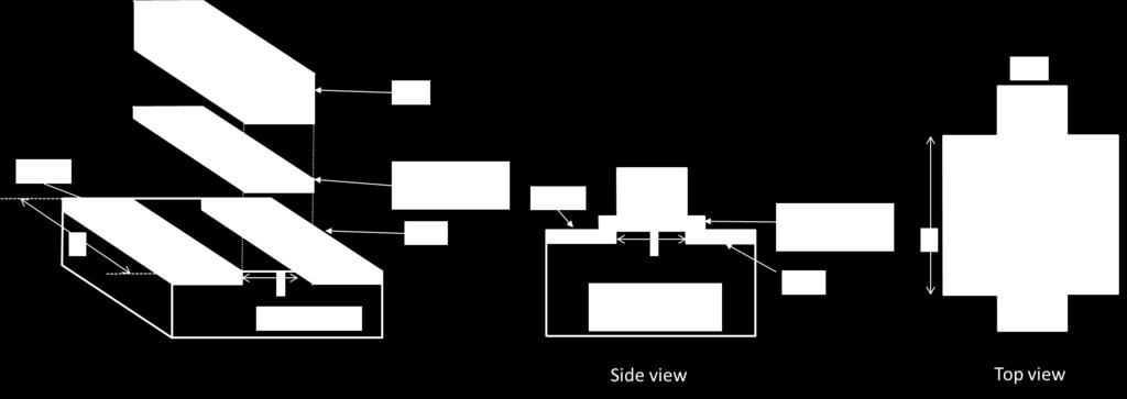
21 Transistor physical diagram
22 Silicon by itself is semiconductor Has 4 valence electrons and forms a co-valent bond with 4 neighbors Hard to break and does not conduct

23 Silicon by itself is insulator Has 4 valence electrons and forms a co-valent bond with 4 neighbors Had to break and does not conduct Silicon + Arsenic makes it filled with electrons and conducting Silicon + Boron makes it filled with holes and conducting

24 nmos and pmos Transistors 3-24
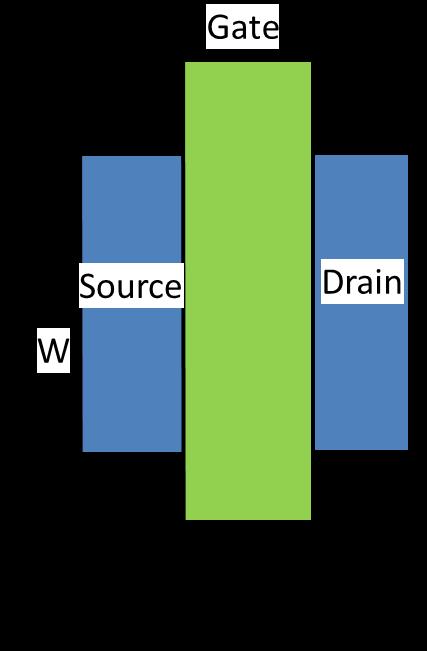
25 Transistor Operation (nmos) Source sets up electric field attracts to boundary Gate-oxide (insulator) Drain n-type n-type p-type Channel
 conductor,")

26 If the figure on the left is a (musical) conductor, then what is the figure on the right? semiconductor 26
27 N-type MOS Transistor MOS = Metal Oxide Semiconductor two types: N-type and P-type N-type when Gate has positive voltage, short circuit between #1 and #2 (switch closed) when Gate has zero voltage, open circuit between #1 and #2 (switch open) Gate = 1 Gate = 0 Terminal #2 must be connected to GND (0V). 3-27
28 P-type MOS Transistor P-type is complementary to N-type when Gate has positive voltage, open circuit between #1 and #2 (switch open) when Gate has zero voltage, short circuit between #1 and #2 (switch closed) Gate = 1 Gate = 0 Terminal #1 must be connected to +2.9V. 3-28
29 Logic Gates Use switch behavior of MOS transistors to implement logical functions: AND, OR, NOT. Digital symbols: recall that we assign a range of analog voltages to each digital (logic) symbol assignment of voltage ranges depends on electrical properties of transistors being used typical values for "1": +5V, +3.3V, +2.9V, +1.1V for purposes of illustration, we'll use +2.9V 3-29
30 CMOS Circuit Complementary MOS Uses both N-type and P-type MOS transistors P-type Attached to + voltage Pulls output voltage UP when input is zero N-type Attached to GND Pulls output voltage DOWN when input is one For all inputs, make sure that output is either connected to GND or to +, but not both! 3-30
31 Transistor Source Output Supply Voltage Gate Gate Gate Drain Ground Output Transistor terminalsn-type transistor Gate Behavior 1 Closed Output=0 0 Open Output=Z P-type transistor Gate Behavior 0 Closed Output=1 1 Open Output=Z
32 NOT Gate with Transistors Vdd Vdd Vdd ON OFF Q A=0 Q=1 A=1 Q=0 OFF ON
33 Inverter (NOT Gate) Truth table In Out 0 V 2.9 V 2.9 V 0 V In Out
34 NOR Gate Note: Serial structure on top, parallel on bottom. A B C
35 OR Gate A B C Add inverter to NOR. 3-35
36 NAND Gate (AND-NOT) Note: Parallel structure on top, serial on bottom. A B C
37 AND Gate A B C Add inverter to NAND. 3-37
38 Basic Logic Gates 3-38
39 In-Class Exercise 1b 8b 23b S Exponent Fraction N 1 S 1.fraction 2 exponent 127, 1 exponent 254 Convert 777 to IEEE 32-bit floating point Convert the results back to decimal 3-39
40 In-Class Exercise 1b 8b 23b S Exponent Fraction N 1 S 1.fraction 2 exponent 127, 1 exponent 254 Convert 777 to IEEE 32-bit floating point 777 = = * 2^9 9 = exp 127 exp = 136 = sign = 0 since positive Convert the results back to decimal 3-40
41 In-Class Exercise 1b 8b 23b S Exponent Fraction N 1 S 1.fraction 2 exponent 127, 1 exponent 254 Convert 777 to IEEE 32-bit floating point Convert the results back to decimal b = 0d136 N = (-1)^S * 1.fraction * 2^(exp-127) N = (-1)^0 * * 2^( ) N = 1* * 2^9 N = N =
42 Take-home exercise Fill out the truth table for the following transistor circuit A B Q
43 Common Misconceptions 3-43
44 More than 2 Inputs? AND/OR can take any number of inputs. AND = 1 if all inputs are 1. OR = 1 if any input is 1. Similar for NAND/NOR. Can implement with multiple two-input gates, or with single CMOS circuit. 3-44
45 Note for all HW2 is due today (1 st Feb) HW3 is out Solutions for HW2 will be posted after HW2 is graded 3-45
46 Note for all Exam 1 will be held on 10 th Feb (Education Sciences 204) 50 min exam NO Books, notes, calculator or electronic devices of any sort 3-46
47 Points Covered so far.. Semiconductor properties of silicon Using silicon to build transistor p type transistor n type transistor Using transistors to build logic gates NAND NOR NOT 3-47

48 Multiple input logic gates 3-input NAND gate with CMOS. 3-48
49 Take-home exercise Fill out the truth table for the following transistor circuit A B Q Q= A (xor) B 3-49
50 Fill out the truth table for the following transistor circuit A B Q
51 Common Misconceptions 3-51
52 Logical Completeness Can implement ANY truth table with AND, OR, NOT. A B C D AND combinations that yield a "1" in the truth table. 2. OR the results of the AND gates. 3-52
53 Practice Implement the following truth table. A B C
54 Practice Implement the following truth table. A B C C= A`B` + A`B + AB` C= A`(B`+B) +AB` C= A` + AB` 3-54
55 DeMorgan's Law Converting AND to OR (with some help from NOT) Consider the following gate: A B A B A B A B To convert AND to OR (or vice versa), invert inputs and output Same as A+B 3-55
56 Half Adder S= A (XOR) B C= AB 3-56
57 Half Adder S= A (XOR) B C= AB 3-57
58 Half Adder S= A (XOR) B C= AB 3-58
59 Fill out the following truth table 3-59
60 Fill out the following truth table 3-60
61 Write the function of Z 3-61
62 Write the function of Z Z= A`B`C` + A`B`C + A`BC` + A`BC + AB`C` 3-62
63 Draw the gate implementation of Z Z= A`+ AB`C` 3-63
64 Gate implementation A` A B` C` 3-64
65 Gate implementation (NAND) A A B` C` 3-65
66 Gate implementation (NOR) A A` B C 3-66
67 Summary MOS transistors are used as switches to implement logic functions. N-type: connect to GND, turn on (with 1) to pull down to 0 P-type: connect to +2.9V, turn on (with 0) to pull up to 1 Basic gates: NOT, NOR, NAND Logic functions are usually expressed with AND, OR, and NOT Properties of logic gates Completeness can implement any truth table with AND, OR, NOT DeMorgan's Law convert AND to OR by inverting inputs and output 3-67

 stores information (state) from past inputs We'll first look at some")
68 Building Functions from Logic Gates We've already seen how to implement truth tables using AND, OR, and NOT -- an example of combinational logic. Combinational Logic Circuit output depends only on the current inputs stateless Sequential Logic Circuit output depends on the sequence of inputs (past and present) stores information (state) from past inputs We'll first look at some useful combinational circuits, then show how to use sequential circuits to store information. 3-68
69 In-class exercise Fill out the truth table for the following transistor circuit Use DeMorgan s Law to simplify NOT(NOT(A) AND (NOT(B) OR C)) A B C output
) NOT(NOT(A)) OR NOT(NOT(B) OR C) A OR (B AND NOT(C)) A B C output 0 0 0 0 0 0 1 0 0 1 0 1 0 1 1 0 1 0 0 1 1 0 1 1 1 1 0 1 1 1 1 1")
70 In-class exercise Fill out the truth table for the following transistor circuit Use DeMorgan s Law to simplify NOT(NOT(A) AND (NOT(B) OR C)) NOT(NOT(A)) OR NOT(NOT(B) OR C) A OR (B AND NOT(C)) A B C output
71 Logical Completeness Can implement ANY truth table with AND, OR, NOT. A B C D AND combinations that yield a "1" in the truth table. 2. OR the results of the AND gates. 3-71
72 Decoder n inputs, 2 n outputs exactly one output is 1 for each possible input pattern 2-bit decoder 3-72
73 Multiplexer (MUX) n-bit selector and 2 n inputs, one output output equals one of the inputs, depending on selector 4-to-1 MUX 3-73
74 Half Adder Add two bits, produce one-bit sum and carry-out. A B S C out
75 Full Adder from Half Adder Add two bits and carry-in, produce one-bit sum and carry-out. A B C in S C out
76 Full Adder Add two bits and carry-in, produce one-bit sum and carry-out. A B C in S C out
77 Four-bit Adder 3-77
78 Combinational vs. Sequential Combinational Circuit always gives the same output for a given set of inputs ex: adder always generates sum and carry, regardless of previous inputs Sequential Circuit stores information output depends on stored information (state) plus input so a given input might produce different outputs, depending on the stored information example: ticket counter advances when you push the button output depends on previous state useful for building memory elements and state machines 3-78
79 In-Class Exercise Find A, B, C, D, E, and F Note: Bits are numbered starting from 0 from right to left. So if X = 10110, then X[4] = 1, X[3] = 0, X[2] = 1, X[1] = 1, and X[0] =

80 In-Class Exercise Solutions Find A, B, C, D, E, and F Note: Bits are numbered starting from 0 from right to left. So if X = 10110, then X[4] = 1, X[3] = 0, X[2] = 1, X[1] = 1, and X[0] = 0. A=0 B=0 C=1 D=0 E=0 F=1 3-80
81 Cross-coupled invertors Good news: holds on to value Bad news: How do we write to it? A Q
82 R-S Latch: Simple Storage Element R is used to reset or clear the element set it to zero. S is used to set the element set it to one out 0 1 out 1 1 If both R and S are one, out could be either zero or one. quiescent state -- holds its previous value note: if a is 1, b is 0, and vice versa 3-82
83 Clearing the R-S latch Suppose we start with output = 1, then change R to zero out Output changes to zero out Then set R=1 to store value in quiescent state. 3-83
84 Setting the R-S Latch Suppose we start with output = 0, then change S to zero out Output changes to one out Then set S=1 to store value in quiescent state. 3-84
85 R-S Latch Summary R = S = 1 hold current value in latch S = 0, R=1 set value to 1 R = 0, S = 1 set value to 0 R = S = 0 both outputs equal one Don t do it! 3-85
86 Gated D-Latch Two inputs: D (data) and WE (write enable) when WE = 1, latch is set to value of D S = NOT(D), R = D when WE = 0, latch holds previous value S = R =
87 Register A register stores a multi-bit value. We use a collection of D-latches, all controlled by a common WE. When WE=1, n-bit value D is written to register. 3-87
88 Representing Multi-bit Values Number bits from right (0) to left (n-1) just a convention -- could be left to right, but must be consistent Use brackets to denote range: D[l:r] denotes bit l to bit r, from left to right A = A[14:9] = A[2:0] = 101 May also see A<14:9>, especially in hardware block diagrams. 3-88
89 Memory Now that we know how to store bits, we can build a memory a logical k m array of stored bits. Address Space: number of locations (usually a power of 2) k = 2 n locations Addressability: number of bits per location (e.g., byte-addressable) m bits 3-89
90 2 2 x 3 Memory address word select word WE input bits write enable address decoder output bits 3-90
91 More Memory Details This is a not the way actual memory is implemented. fewer transistors, much more dense, relies on electrical properties But the logical structure is very similar. address decoder word select line word write enable Also, non-volatile memories: ROM, PROM, flash, 3-91
 slower but denser, bit storage must be periodically refreshed Also, non-volatile memories: ROM, PROM,")
92 More Memory Details Two basic kinds of RAM (Random Access Memory) Static RAM (SRAM) fast, maintains data without power Dynamic RAM (DRAM) slower but denser, bit storage must be periodically refreshed Also, non-volatile memories: ROM, PROM, flash, 3-92
93 In-class Exercise Specify the value of "out" signal for each set of inputs for the RS latch. Time S R out 0 0 Specify the value of "out" signal for each set of inputs for the gated d-latch. Time D WE out
94 In-class Exercise Solution Specify the value of "out" signal for each set of inputs for the RS latch. Time S R out Specify the value of "out" signal for each set of inputs for the gated d-latch. Time D WE out
95 In-class Exercise Solutions Specify the value of "out" signal for each set of inputs for the RS latch. Time S R out Specify the value of "out" signal for each set of inputs for the gated d-latch. Time D WE out
96 Combinational vs. Sequential Two types of locks Combinational Success depends only on the values, not the order in which they are set. Sequential Success depends on the sequence of values (e.g, R-13, L-22, R-3). 3-96
97 Points Covered Decoder n input (2^n) output decoder asserts exactly one of its output bits 3-97
98 Points Covered Using two 3-to-8 decoder to get 4- to-16 decoder 3-98
99 Points Covered Multiplexer Combinational circuits and Sequential circuits Using logic gates to make storage elements Feedback path RS latch D latch 3-99
100 R-S Latch Summary R = S = 1 hold current value in latch S = 0, R=1 set value to 1 R = 0, S = 1 set value to 0 R = S = 0 both outputs equal one Don t do it! 3-100
101 D Latch Summary D = X, WE=0 ( X-> Don t care) hold current value in latch D = 1, WE=1 set value to 1 D = 0, WE=1 set value to
 based on inputs and current state State Machine Inputs Combinational Logic Circuit Outputs Storage")
102 State Machine Another type of sequential circuit Combines combinational logic with storage Remembers state, and changes output (and state) based on inputs and current state State Machine Inputs Combinational Logic Circuit Outputs Storage Elements 3-102
103 State The state of a system is a snapshot of all the relevant elements of the system at the moment the snapshot is taken. Examples: The state of a basketball game can be represented by the scoreboard. Number of points, time remaining, possession, etc. The state of a tic-tac-toe game can be represented by the placement of X s and O s on the board, and who's turn it is
104 Sequential Lock Two types of locks Combinational Success depends only on the values, not the order in which they are set. Sequential Success depends on the sequence of values (e.g, R-13, L-22, R-3)
105 State of Sequential Lock Our lock example has four different states, labelled A-D: A: The lock is not open, and no relevant operations have been performed. B: The lock is not open, and the user has completed the R-13 operation. C: The lock is not open, and the user has completed R-13, followed by L-22. D: The lock is open, and the user has completed R-13, followed by L-22, followed by R
106 State Diagram Shows states and actions that cause a transition between states. closed closed other than R-13 and R-13 open closed 3-106
107 Finite State Machine A description of a system with the following components: 1. A finite number of states 2. A finite number of external inputs 3. A finite number of external outputs 4. An explicit specification of all state transitions 5. An explicit specification of what causes each external output value. Often described by a state diagram. Inputs may cause state transitions. Outputs are associated with each state (or with each transition)
108 The Clock Frequently, a clock circuit triggers transition from one state to the next. 1 0 One Cycle time At the beginning of each clock cycle, state machine makes a transition, based on the current state and the external inputs. Not always required. In lock example, the input itself triggers a transition
109 Implementing a Finite State Machine Combinational logic Determine outputs and next state. Storage elements Maintain state representation. State Machine Inputs Combinational Logic Circuit Outputs Clock Storage Elements 3-109
110 Storage: Master-Slave Flipflop A pair of gated D-latches, to isolate next state from current state. During 1 st phase (clock=1), previously-computed state becomes current state and is sent to the logic circuit. During 2 nd phase (clock=0), next state, computed by logic circuit, is stored in Latch A

111 Storage: Master-Slave Flipflop 3-111
112 In-class Exercise Specify the value of Q0 and Q1 signal for each set of inputs for the master-slave flipflop. Time Clock Din Q0 0 1 Q

113 In-class Exercise Solutions Specify the value of Q0 and Q1 signal for each set of inputs for the master-slave flipflop. Time Clock Din Q Q
114 In-class Exercise 1 Copyright The McGraw-Hill Companies, Inc. Permission required for reproduction or display. Specify the next State and Out for each set of inputs. Time State Input Output
115 In-class Exercise 1 Solutions Specify the next State and Out for each set of inputs. Time State Input Output
116 Storage Each master-slave flipflop stores one state bit. Examples: Sequential lock Four states two bits State Machine Inputs Combinational Logic Circuit Outputs Clock Storage Elements 3-116
117 In-class Exercise 2 Given the clock/enable and data signal, specify the Latch and Flip-Flop signal


118 In-class Exercise 2 Solutions Given the clock/enable and data signal, specify the Latch and Flip-Flop signal
119 Complete Example A blinking traffic sign No lights on 1 & 2 on 1, 2, 3, & 4 on 1, 2, 3, 4, & 5 on (repeat as long as switch is turned on) 2 DANGER MOVE RIGHT 3-119
120 Complete Example A blinking traffic sign No lights on 1 & 2 on 1, 2, 3, & 4 on 1, 2, 3, 4, & 5 on (repeat as long as switch is turned on) 2 DANGER MOVE RIGHT 3-120
121 Complete Example A blinking traffic sign No lights on 1 & 2 on 1, 2, 3, & 4 on 1, 2, 3, 4, & 5 on (repeat as long as switch is turned on) 2 DANGER MOVE RIGHT 3-121
122 Complete Example A blinking traffic sign No lights on 1 & 2 on 1, 2, 3, & 4 on 1, 2, 3, 4, & 5 on (repeat as long as switch is turned on) 2 DANGER MOVE RIGHT 3-122
123 Complete Example A blinking traffic sign No lights on 1 & 2 on 1, 2, 3, & 4 on 1, 2, 3, 4, & 5 on (repeat as long as switch is turned on) 2 DANGER MOVE RIGHT 3-123
124 Complete Example A blinking traffic sign No lights on 1 & 2 on 1, 2, 3, & 4 on 1, 2, 3, 4, & 5 on (repeat as long as switch is turned on) 2 DANGER MOVE RIGHT 3-124
125 Complete Example A blinking traffic sign No lights on 1 & 2 on 1, 2, 3, & 4 on 1, 2, 3, 4, & 5 on (repeat as long as switch is turned on) 2 DANGER MOVE RIGHT 3-125
126 Complete Example A blinking traffic sign No lights on 1 & 2 on 1, 2, 3, & 4 on 1, 2, 3, 4, & 5 on (repeat as long as switch is turned on) 2 DANGER MOVE RIGHT 3-126
127 Complete Example A blinking traffic sign No lights on 1 & 2 on 1, 2, 3, & 4 on 1, 2, 3, 4, & 5 on (repeat as long as switch is turned on) 2 DANGER MOVE RIGHT 3-127
128 Complete Example A blinking traffic sign No lights on 1 & 2 on 1, 2, 3, & 4 on 1, 2, 3, 4, & 5 on (repeat as long as switch is turned on) 2 DANGER MOVE RIGHT 3-128
129 Complete Example A blinking traffic sign No lights on 1 & 2 on 1, 2, 3, & 4 on 1, 2, 3, 4, & 5 on (repeat as long as switch is turned on) 2 DANGER MOVE RIGHT 3-129
130 Complete Example A blinking traffic sign No lights on 1 & 2 on 1, 2, 3, & 4 on 1, 2, 3, 4, & 5 on (repeat as long as switch is turned on) 2 DANGER MOVE RIGHT 3-130
131 Traffic Sign State Diagram Switch off Switch on State bit S 1 State bit S 0 Outputs Transition on each clock cycle
132 Traffic Sign Truth Tables Outputs (depend only on state: S 1 S 0 ) Lights 1 and 2 Lights 3 and 4 Light 5 Next State: S 1 S 0 (depend on state and input) Switch In S 1 S 0 S 1 S 0 S 1 S 0 Z Y X Whenever In=0, next state is X X
133 Traffic Sign Logic Master-slave flipflop 3-133
134 From Logic to Data Path The data path of a computer is all the logic used to process information. See the data path of the LC-3 on next slide. Combinational Logic Decoders -- convert instructions into control signals Multiplexers -- select inputs and outputs ALU (Arithmetic and Logic Unit) -- operations on data Sequential Logic State machine -- coordinate control signals and data movement Registers and latches -- storage elements 3-134
135 LC-3 Data Path 3-135
Introduction to Computer Engineering. CS/ECE 252, Fall 2012 Prof. Guri Sohi Computer Sciences Department University of Wisconsin Madison
 Introduction to Computer Engineering CS/ECE 252, Fall 2012 Prof. Guri Sohi Computer Sciences Department University of Wisconsin Madison Chapter 3 Digital Logic Structures Slides based on set prepared by
CMPE12 - Notes chapter 1. Digital Logic. (Textbook Chapter 3)
") CMPE12 - Notes chapter 1 Digital Logic (Textbook Chapter 3) Transistor: Building Block of Computers Microprocessors contain TONS of transistors Intel Montecito (2005): 1.72 billion Intel Pentium 4 (2000):
CMPE12 - Notes chapter 1 Digital Logic (Textbook Chapter 3) Transistor: Building Block of Computers Microprocessors contain TONS of transistors Intel Montecito (2005): 1.72 billion Intel Pentium 4 (2000):
Chapter 3 Digital Logic Structures
 Chapter 3 Digital Logic Structures Original slides from Gregory Byrd, North Carolina State University Modified by C. Wilcox, M. Strout, Y. Malaiya Colorado State University Computing Layers Problems Algorithms
Digital Logic. CS211 Computer Architecture. l Topics. l Transistors (Design & Types) l Logic Gates. l Combinational Circuits.
 l Logic Gates. l Combinational Circuits.") CS211 Computer Architecture Digital Logic l Topics l Transistors (Design & Types) l Logic Gates l Combinational Circuits l K-Maps Figures & Tables borrowed from:! http://www.allaboutcircuits.com/vol_4/index.html!
CS211 Computer Architecture Digital Logic l Topics l Transistors (Design & Types) l Logic Gates l Combinational Circuits l K-Maps Figures & Tables borrowed from:! http://www.allaboutcircuits.com/vol_4/index.html!
CMPE12 - Notes chapter 2. Digital Logic. (Textbook Chapters and 2.1)"
") CMPE12 - Notes chapter 2 Digital Logic (Textbook Chapters 3.1-3.5 and 2.1)" Truth table" The most basic representation of a logic function." Brute force representation listing the output for all possible
CMPE12 - Notes chapter 2 Digital Logic (Textbook Chapters 3.1-3.5 and 2.1)" Truth table" The most basic representation of a logic function." Brute force representation listing the output for all possible
Combinational vs. Sequential. Summary of Combinational Logic. Combinational device/circuit: any circuit built using the basic gates Expressed as
 Summary of Combinational Logic : Computer Architecture I Instructor: Prof. Bhagi Narahari Dept. of Computer Science Course URL: www.seas.gwu.edu/~bhagiweb/cs3/ Combinational device/circuit: any circuit
Floating Point Representation and Digital Logic. Lecture 11 CS301
 Floating Point Representation and Digital Logic Lecture 11 CS301 Administrative Daily Review of today s lecture w Due tomorrow (10/4) at 8am Lab #3 due Friday (9/7) 1:29pm HW #5 assigned w Due Monday 10/8
Lecture 22 Chapters 3 Logic Circuits Part 1
 Lecture 22 Chapters 3 Logic Circuits Part 1 LC-3 Data Path Revisited How are the components Seen here implemented? 5-2 Computing Layers Problems Algorithms Language Instruction Set Architecture Microarchitecture
Digital Logic: Boolean Algebra and Gates. Textbook Chapter 3
 Digital Logic: Boolean Algebra and Gates Textbook Chapter 3 Basic Logic Gates XOR CMPE12 Summer 2009 02-2 Truth Table The most basic representation of a logic function Lists the output for all possible
LOGIC CIRCUITS. Basic Experiment and Design of Electronics. Ho Kyung Kim, Ph.D.
 Basic Experiment and Design of Electronics LOGIC CIRCUITS Ho Kyung Kim, Ph.D. hokyung@pusan.ac.kr School of Mechanical Engineering Pusan National University Digital IC packages TTL (transistor-transistor
Organisasi dan Arsitektur Komputer L#1: Fundamental Concepts Amil A. Ilham
 Organisasi dan Arsitektur Komputer http://www.unhas.ac.id/amil/stmik2016/arsikom/ L#1: Fundamental Concepts Amil A. Ilham http://www.unhas.ac.id/amil Administrasi Kuliah ADMINISTRASI KULIAH 2 Penilaian
ALU A functional unit
 ALU A functional unit that performs arithmetic operations such as ADD, SUB, MPY logical operations such as AND, OR, XOR, NOT on given data types: 8-,16-,32-, or 64-bit values A n-1 A n-2... A 1 A 0 B n-1
EE40 Lec 15. Logic Synthesis and Sequential Logic Circuits
 EE40 Lec 15 Logic Synthesis and Sequential Logic Circuits Prof. Nathan Cheung 10/20/2009 Reading: Hambley Chapters 7.4-7.6 Karnaugh Maps: Read following before reading textbook http://www.facstaff.bucknell.edu/mastascu/elessonshtml/logic/logic3.html
LOGIC CIRCUITS. Basic Experiment and Design of Electronics
 Basic Experiment and Design of Electronics LOGIC CIRCUITS Ho Kyung Kim, Ph.D. hokyung@pusan.ac.kr School of Mechanical Engineering Pusan National University Outline Combinational logic circuits Output
Chapter 7. Sequential Circuits Registers, Counters, RAM
 Chapter 7. Sequential Circuits Registers, Counters, RAM Register - a group of binary storage elements suitable for holding binary info A group of FFs constitutes a register Commonly used as temporary storage
UNIVERSITY OF WISCONSIN MADISON
 CS/ECE 252: INTRODUCTION TO COMPUTER ENGINEERING UNIVERSITY OF WISCONSIN MADISON Prof. Gurindar Sohi TAs: Minsub Shin, Lisa Ossian, Sujith Surendran Midterm Examination 2 In Class (50 minutes) Friday,
Boolean Algebra and Digital Logic 2009, University of Colombo School of Computing
 IT 204 Section 3.0 Boolean Algebra and Digital Logic Boolean Algebra 2 Logic Equations to Truth Tables X = A. B + A. B + AB A B X 0 0 0 0 3 Sum of Products The OR operation performed on the products of
Latches. October 13, 2003 Latches 1
 Latches The second part of CS231 focuses on sequential circuits, where we add memory to the hardware that we ve already seen. Our schedule will be very similar to before: We first show how primitive memory
Sequential Logic. Rab Nawaz Khan Jadoon DCS. Lecturer COMSATS Lahore Pakistan. Department of Computer Science
 Sequential Logic Rab Nawaz Khan Jadoon DCS COMSATS Institute of Information Technology Lecturer COMSATS Lahore Pakistan Digital Logic and Computer Design Sequential Logic Combinational circuits with memory
Topics. Dynamic CMOS Sequential Design Memory and Control. John A. Chandy Dept. of Electrical and Computer Engineering University of Connecticut
 Topics Dynamic CMOS Sequential Design Memory and Control Dynamic CMOS In static circuits at every point in time (except when switching) the output is connected to either GND or V DD via a low resistance
Fundamentals of Digital Design
 Fundamentals of Digital Design Digital Radiation Measurement and Spectroscopy NE/RHP 537 1 Binary Number System The binary numeral system, or base-2 number system, is a numeral system that represents numeric
ESE 570: Digital Integrated Circuits and VLSI Fundamentals
 ESE 570: Digital Integrated Circuits and VLSI Fundamentals Lec 21: April 4, 2017 Memory Overview, Memory Core Cells Penn ESE 570 Spring 2017 Khanna Today! Memory " Classification " ROM Memories " RAM Memory
DIGITAL LOGIC CIRCUITS
 DIGITAL LOGIC CIRCUITS Introduction Logic Gates Boolean Algebra Map Specification Combinational Circuits Flip-Flops Sequential Circuits Memory Components Integrated Circuits Digital Computers 2 LOGIC GATES
 vidyarthiplus.com vidyarthiplus.com vidyarthiplus.com ANNA UNIVERSITY- COMBATORE B.E./ B.TECH. DEGREE EXAMINATION - JUNE 2009. ELECTRICAL & ELECTONICS ENGG. - FOURTH SEMESTER DIGITAL LOGIC CIRCUITS PART-A
SIR C.R.REDDY COLLEGE OF ENGINEERING ELURU DIGITAL INTEGRATED CIRCUITS (DIC) LABORATORY MANUAL III / IV B.E. (ECE) : I - SEMESTER
 LABORATORY MANUAL III / IV B.E. (ECE) : I - SEMESTER") SIR C.R.REDDY COLLEGE OF ENGINEERING ELURU 534 007 DIGITAL INTEGRATED CIRCUITS (DIC) LABORATORY MANUAL III / IV B.E. (ECE) : I - SEMESTER DEPARTMENT OF ELECTRONICS AND COMMUNICATION ENGINEERING DIGITAL
SIR C.R.REDDY COLLEGE OF ENGINEERING ELURU 534 007 DIGITAL INTEGRATED CIRCUITS (DIC) LABORATORY MANUAL III / IV B.E. (ECE) : I - SEMESTER DEPARTMENT OF ELECTRONICS AND COMMUNICATION ENGINEERING DIGITAL
Digital Integrated Circuits A Design Perspective
 Semiconductor Memories Adapted from Chapter 12 of Digital Integrated Circuits A Design Perspective Jan M. Rabaey et al. Copyright 2003 Prentice Hall/Pearson Outline Memory Classification Memory Architectures
E40M. Binary Numbers. M. Horowitz, J. Plummer, R. Howe 1
 E40M Binary Numbers M. Horowitz, J. Plummer, R. Howe 1 Reading Chapter 5 in the reader A&L 5.6 M. Horowitz, J. Plummer, R. Howe 2 Useless Box Lab Project #2 Adding a computer to the Useless Box alows us
Introduction to CMOS VLSI Design Lecture 1: Introduction
 Introduction to CMOS VLSI Design Lecture 1: Introduction David Harris, Harvey Mudd College Kartik Mohanram and Steven Levitan University of Pittsburgh Introduction Integrated circuits: many transistors
DE58/DC58 LOGIC DESIGN DEC 2014
 Q.2 a. In a base-5 number system, 3 digit representations is used. Find out (i) Number of distinct quantities that can be represented.(ii) Representation of highest decimal number in base-5. Since, r=5
Semiconductor memories
 Semiconductor memories Semiconductor Memories Data in Write Memory cell Read Data out Some design issues : How many cells? Function? Power consuption? Access type? How fast are read/write operations? Semiconductor
ESE 570: Digital Integrated Circuits and VLSI Fundamentals
 ESE 570: Digital Integrated Circuits and VLSI Fundamentals Lec 19: March 29, 2018 Memory Overview, Memory Core Cells Today! Charge Leakage/Charge Sharing " Domino Logic Design Considerations! Logic Comparisons!
Intro To Digital Logic
 Intro To Digital Logic 1 Announcements... Project 2.2 out But delayed till after the midterm Midterm in a week Covers up to last lecture + next week's homework & lab Nick goes "H-Bomb of Justice" About
Semiconductor Memory Classification
 Semiconductor Memory Classification Read-Write Memory Non-Volatile Read-Write Memory Read-Only Memory Random Access Non-Random Access EPROM E 2 PROM Mask-Programmed Programmable (PROM) SRAM FIFO FLASH
Memory, Latches, & Registers
 Memory, Latches, & Registers 1) Structured Logic Arrays 2) Memory Arrays 3) Transparent Latches 4) How to save a few bucks at toll booths 5) Edge-triggered Registers L13 Memory 1 General Table Lookup Synthesis
UNIVERSITY OF BOLTON SCHOOL OF ENGINEERING BENG (HONS) ELECTRICAL & ELECTRONICS ENGINEERING EXAMINATION SEMESTER /2017
 ELECTRICAL & ELECTRONICS ENGINEERING EXAMINATION SEMESTER /2017") UNIVERSITY OF BOLTON TW35 SCHOOL OF ENGINEERING BENG (HONS) ELECTRICAL & ELECTRONICS ENGINEERING EXAMINATION SEMESTER 2-2016/2017 INTERMEDIATE DIGITAL ELECTRONICS AND COMMUNICATIONS MODULE NO: EEE5002
UNIVERSITY OF BOLTON TW35 SCHOOL OF ENGINEERING BENG (HONS) ELECTRICAL & ELECTRONICS ENGINEERING EXAMINATION SEMESTER 2-2016/2017 INTERMEDIATE DIGITAL ELECTRONICS AND COMMUNICATIONS MODULE NO: EEE5002
! Charge Leakage/Charge Sharing. " Domino Logic Design Considerations. ! Logic Comparisons. ! Memory. " Classification. " ROM Memories.
 ESE 57: Digital Integrated Circuits and VLSI Fundamentals Lec 9: March 9, 8 Memory Overview, Memory Core Cells Today! Charge Leakage/ " Domino Logic Design Considerations! Logic Comparisons! Memory " Classification
Lecture 7: Logic design. Combinational logic circuits
 /24/28 Lecture 7: Logic design Binary digital circuits: Two voltage levels: and (ground and supply voltage) Built from transistors used as on/off switches Analog circuits not very suitable for generic
Digital Integrated Circuits A Design Perspective. Semiconductor. Memories. Memories
 Digital Integrated Circuits A Design Perspective Semiconductor Chapter Overview Memory Classification Memory Architectures The Memory Core Periphery Reliability Case Studies Semiconductor Memory Classification
Introduction to Computer Engineering ECE 203
 Introduction to Computer Engineering ECE 203 Northwestern University Department of Electrical Engineering and Computer Science Teacher: Robert Dick Office: L477 Tech Email: dickrp@ece.northwestern.edu
University of Toronto Faculty of Applied Science and Engineering Edward S. Rogers Sr. Department of Electrical and Computer Engineering
 University of Toronto Faculty of Applied Science and Engineering Edward S. Rogers Sr. Department of Electrical and Computer Engineering Final Examination ECE 241F - Digital Systems Examiners: J. Rose and
Sample Test Paper - I
 Scheme G Sample Test Paper - I Course Name : Computer Engineering Group Marks : 25 Hours: 1 Hrs. Q.1) Attempt any THREE: 09 Marks a) Define i) Propagation delay ii) Fan-in iii) Fan-out b) Convert the following:
Unit II Chapter 4:- Digital Logic Contents 4.1 Introduction... 4
 Unit II Chapter 4:- Digital Logic Contents 4.1 Introduction... 4 4.1.1 Signal... 4 4.1.2 Comparison of Analog and Digital Signal... 7 4.2 Number Systems... 7 4.2.1 Decimal Number System... 7 4.2.2 Binary
Reg. No. Question Paper Code : B.E./B.Tech. DEGREE EXAMINATION, NOVEMBER/DECEMBER Second Semester. Computer Science and Engineering
 Sp 6 Reg. No. Question Paper Code : 27156 B.E./B.Tech. DEGREE EXAMINATION, NOVEMBER/DECEMBER 2015. Second Semester Computer Science and Engineering CS 6201 DIGITAL PRINCIPLES AND SYSTEM DESIGN (Common
MODEL ANSWER SUMMER 17 EXAMINATION Subject Title: Principles of Digital Techniques
 MODEL ANSWER SUMMER 17 EXAMINATION Subject Title: Principles of Digital Techniques Subject Code: Important Instructions to examiners: 1) The answers should be examined by key words and not as word-to-word
ECE 250 / CPS 250 Computer Architecture. Basics of Logic Design Boolean Algebra, Logic Gates
 ECE 250 / CPS 250 Computer Architecture Basics of Logic Design Boolean Algebra, Logic Gates Benjamin Lee Slides based on those from Andrew Hilton (Duke), Alvy Lebeck (Duke) Benjamin Lee (Duke), and Amir
Semiconductor Memories
 Semiconductor References: Adapted from: Digital Integrated Circuits: A Design Perspective, J. Rabaey UCB Principles of CMOS VLSI Design: A Systems Perspective, 2nd Ed., N. H. E. Weste and K. Eshraghian
ELCT201: DIGITAL LOGIC DESIGN
 ELCT201: DIGITAL LOGIC DESIGN Dr. Eng. Haitham Omran, haitham.omran@guc.edu.eg Dr. Eng. Wassim Alexan, wassim.joseph@guc.edu.eg Lecture 6 Following the slides of Dr. Ahmed H. Madian محرم 1439 ه Winter
Lecture 34: Portable Systems Technology Background Professor Randy H. Katz Computer Science 252 Fall 1995
 Lecture 34: Portable Systems Technology Background Professor Randy H. Katz Computer Science 252 Fall 1995 RHK.F95 1 Technology Trends: Microprocessor Capacity 100000000 10000000 Pentium Transistors 1000000
S.Y. Diploma : Sem. III [DE/ED/EI/EJ/EN/ET/EV/EX/IC/IE/IS/IU/MU] Principles of Digital Techniques
![S.Y. Diploma : Sem. III [DE/ED/EI/EJ/EN/ET/EV/EX/IC/IE/IS/IU/MU] Principles of Digital Techniques](/thumbs/82/86792063.jpg "S.Y. Diploma : Sem. III [DE/ED/EI/EJ/EN/ET/EV/EX/IC/IE/IS/IU/MU] Principles of Digital Techniques") S.Y. Diploma : Sem. III [DE/ED/EI/EJ/EN/ET/EV/EX/IC/IE/IS/IU/MU] Principles of Digital Techniques Time: 3 Hrs.] Prelim Question Paper Solution [Marks : 100 Q.1(a) Attempt any SIX of the following : [12]
S.Y. Diploma : Sem. III [DE/ED/EI/EJ/EN/ET/EV/EX/IC/IE/IS/IU/MU] Principles of Digital Techniques Time: 3 Hrs.] Prelim Question Paper Solution [Marks : 100 Q.1(a) Attempt any SIX of the following : [12]
ECE/CS 250 Computer Architecture
 ECE/CS 250 Computer Architecture Basics of Logic Design: Boolean Algebra, Logic Gates (Combinational Logic) Tyler Bletsch Duke University Slides are derived from work by Daniel J. Sorin (Duke), Alvy Lebeck
MAHARASHTRA STATE BOARD OF TECHNICAL EDUCATION (Autonomous) (ISO/IEC Certified)
 (ISO/IEC Certified)") WINTER 17 EXAMINATION Subject Name: Digital Techniques Model Answer Subject Code: 17333 Important Instructions to examiners: 1) The answers should be examined by key words and not as word-to-word as given
WINTER 17 EXAMINATION Subject Name: Digital Techniques Model Answer Subject Code: 17333 Important Instructions to examiners: 1) The answers should be examined by key words and not as word-to-word as given
on candidate s understanding. 7) For programming language papers, credit may be given to any other program based on equivalent concept.
 For programming language papers, credit may be given to any other program based on equivalent concept.") WINTER 17 EXAMINATION Subject Name: Digital Techniques Model Answer Subject Code: 17333 Important Instructions to examiners: 1) The answers should be examined by key words and not as word-to-word as given
WINTER 17 EXAMINATION Subject Name: Digital Techniques Model Answer Subject Code: 17333 Important Instructions to examiners: 1) The answers should be examined by key words and not as word-to-word as given
Hw 6 and 7 Graded and available Project Phase 2 Graded Project Phase 3 Launch Today
 EECS141 1 Hw 8 Posted Last one to be graded Due Friday April 30 Hw 6 and 7 Graded and available Project Phase 2 Graded Project Phase 3 Launch Today EECS141 2 1 6 5 4 3 2 1 0 1.5 2 2.5 3 3.5 4 Frequency
SUMMER 18 EXAMINATION Subject Name: Principles of Digital Techniques Model Answer Subject Code:
 Important Instructions to examiners: 1) The answers should be examined by key words and not as word-to-word as given in the model answer scheme. 2) The model answer and the answer written by candidate
CMOS Digital Integrated Circuits Lec 13 Semiconductor Memories
 Lec 13 Semiconductor Memories 1 Semiconductor Memory Types Semiconductor Memories Read/Write (R/W) Memory or Random Access Memory (RAM) Read-Only Memory (ROM) Dynamic RAM (DRAM) Static RAM (SRAM) 1. Mask
Combinational Logic Trainer Lab Manual
 Combinational Logic Trainer Lab Manual Control Inputs Microprocessor Data Inputs ff Control Unit '0' Datapath MUX Nextstate Logic State Memory Register Output Logic Control Signals ALU ff Register Status
S No. Questions Bloom s Taxonomy Level UNIT-I
 GROUP-A (SHORT ANSWER QUESTIONS) S No. Questions Bloom s UNIT-I 1 Define oxidation & Classify different types of oxidation Remember 1 2 Explain about Ion implantation Understand 1 3 Describe lithography
Adders, subtractors comparators, multipliers and other ALU elements
 CSE4: Components and Design Techniques for Digital Systems Adders, subtractors comparators, multipliers and other ALU elements Adders 2 Circuit Delay Transistors have instrinsic resistance and capacitance
ESE 570: Digital Integrated Circuits and VLSI Fundamentals
 ESE 570: Digital Integrated Circuits and VLSI Fundamentals Lec 17: March 23, 2017 Energy and Power Optimization, Design Space Exploration, Synchronous MOS Logic Lecture Outline! Energy and Power Optimization
EE241 - Spring 2000 Advanced Digital Integrated Circuits. References
 EE241 - Spring 2000 Advanced Digital Integrated Circuits Lecture 26 Memory References Rabaey, Digital Integrated Circuits Memory Design and Evolution, VLSI Circuits Short Course, 1998.» Gillingham, Evolution
Number System. Decimal to binary Binary to Decimal Binary to octal Binary to hexadecimal Hexadecimal to binary Octal to binary
 Number System Decimal to binary Binary to Decimal Binary to octal Binary to hexadecimal Hexadecimal to binary Octal to binary BOOLEAN ALGEBRA BOOLEAN LOGIC OPERATIONS Logical AND Logical OR Logical COMPLEMENTATION
Section 3: Combinational Logic Design. Department of Electrical Engineering, University of Waterloo. Combinational Logic
 Section 3: Combinational Logic Design Major Topics Design Procedure Multilevel circuits Design with XOR gates Adders and Subtractors Binary parallel adder Decoders Encoders Multiplexers Programmed Logic
Sequential vs. Combinational
 Sequential Circuits Sequential vs. Combinational Combinational Logic: Output depends only on current input TV channel selector (-9) inputs system outputs Sequential Logic: Output depends not only on current
Department of Electrical & Electronics EE-333 DIGITAL SYSTEMS
 Department of Electrical & Electronics EE-333 DIGITAL SYSTEMS 1) Given the two binary numbers X = 1010100 and Y = 1000011, perform the subtraction (a) X -Y and (b) Y - X using 2's complements. a) X = 1010100
Adders allow computers to add numbers 2-bit ripple-carry adder
 Lecture 12 Logistics HW was due yesterday HW5 was out yesterday (due next Wednesday) Feedback: thank you! Things to work on: ig picture, ook chapters, Exam comments Last lecture dders Today Clarification
ECE321 Electronics I
 ECE321 Electronics I Lecture 1: Introduction to Digital Electronics Payman Zarkesh-Ha Office: ECE Bldg. 230B Office hours: Tuesday 2:00-3:00PM or by appointment E-mail: payman@ece.unm.edu Slide: 1 Textbook
Dynamic Combinational Circuits. Dynamic Logic
 Dynamic Combinational Circuits Dynamic circuits Charge sharing, charge redistribution Domino logic np-cmos (zipper CMOS) Krish Chakrabarty 1 Dynamic Logic Dynamic gates use a clocked pmos pullup Two modes:
CSC9R6 Computer Design. Practical Digital Logic
 CSC9R6 Computer Design Practical Digital Logic 1 References (for this part of CSC9R6) Hamacher et al: Computer Organization App A. In library Floyd: Digital Fundamentals Ch 1, 3-6, 8-10 web page: www.prenhall.com/floyd/
Appendix B. Review of Digital Logic. Baback Izadi Division of Engineering Programs
 Appendix B Review of Digital Logic Baback Izadi Division of Engineering Programs bai@engr.newpaltz.edu Elect. & Comp. Eng. 2 DeMorgan Symbols NAND (A.B) = A +B NOR (A+B) = A.B AND A.B = A.B = (A +B ) OR
CHW 261: Logic Design
 CHW 26: Logic Design Instructors: Prof. Hala Zayed Dr. Ahmed Shalaby http://www.bu.edu.eg/staff/halazayed4 http://bu.edu.eg/staff/ahmedshalaby4# Slide Digital Fundamentals Digital Concepts Slide 2 What?
MAHARASHTRA STATE BOARD OF TECHNICAL EDUCATION (Autonomous) (ISO/IEC Certified) SUMMER 14 EXAMINATION Model Answer
 (ISO/IEC Certified) SUMMER 14 EXAMINATION Model Answer") MAHARASHTRA STATE BOARD OF TECHNICAL EDUCATION (Autonomous) (ISO/IEC 27001 2005 Certified) SUMMER 14 EXAMINATION Model Answer Subject Code : 17320 Page No: 1/34 Important Instructions to examiners: 1)
MAHARASHTRA STATE BOARD OF TECHNICAL EDUCATION (Autonomous) (ISO/IEC 27001 2005 Certified) SUMMER 14 EXAMINATION Model Answer Subject Code : 17320 Page No: 1/34 Important Instructions to examiners: 1)
Adders, subtractors comparators, multipliers and other ALU elements
 CSE4: Components and Design Techniques for Digital Systems Adders, subtractors comparators, multipliers and other ALU elements Instructor: Mohsen Imani UC San Diego Slides from: Prof.Tajana Simunic Rosing
Topics. CMOS Design Multi-input delay analysis. John A. Chandy Dept. of Electrical and Computer Engineering University of Connecticut
 Topics CMO Design Multi-input delay analysis pring 25 Transmission Gate OUT Z OUT Z pring 25 Transmission Gate OUT When is low, the output is at high impedance When is high, the output follows However,
University of Toronto Faculty of Applied Science and Engineering Final Examination
 University of Toronto Faculty of Applied Science and Engineering Final Examination ECE 24S - Digital Systems Examiner: Belinda Wang, Jianwen Zhu 2: - 4:3pm, April 26th, 24 Duration: 5 minutes (2.5 hours)
CS/COE0447: Computer Organization
 CS/COE0447: Computer Organization and Assembly Language Logic Design Review Sangyeun Cho Dept. of Computer Science Logic design? Digital hardware is implemented by way of logic design Digital circuits
CS470: Computer Architecture. AMD Quad Core
 CS470: Computer Architecture Yashwant K. Malaiya, Professor malaiya@cs.colostate.edu AMD Quad Core 1 Architecture Layers Building blocks Gates, flip-flops Functional bocks: Combinational, Sequential Instruction
CprE 281: Digital Logic
 CprE 28: Digital Logic Instructor: Alexander Stoytchev http://www.ece.iastate.edu/~alexs/classes/ Simple Processor CprE 28: Digital Logic Iowa State University, Ames, IA Copyright Alexander Stoytchev Digital
! Memory. " RAM Memory. ! Cell size accounts for most of memory array size. ! 6T SRAM Cell. " Used in most commercial chips
 ESE 57: Digital Integrated Circuits and VLSI Fundamentals Lec : April 3, 8 Memory: Core Cells Today! Memory " RAM Memory " Architecture " Memory core " SRAM " DRAM " Periphery Penn ESE 57 Spring 8 - Khanna
Lecture 25. Semiconductor Memories. Issues in Memory
 Lecture 25 Semiconductor Memories Issues in Memory Memory Classification Memory Architectures TheMemoryCore Periphery 1 Semiconductor Memory Classification RWM NVRWM ROM Random Access Non-Random Access
We are here. Assembly Language. Processors Arithmetic Logic Units. Finite State Machines. Circuits Gates. Transistors
 CSC258 Week 3 1 Logistics If you cannot login to MarkUs, email me your UTORID and name. Check lab marks on MarkUs, if it s recorded wrong, contact Larry within a week after the lab. Quiz 1 average: 86%
ECE/CS 250: Computer Architecture. Basics of Logic Design: Boolean Algebra, Logic Gates. Benjamin Lee
 ECE/CS 250: Computer Architecture Basics of Logic Design: Boolean Algebra, Logic Gates Benjamin Lee Slides based on those from Alvin Lebeck, Daniel Sorin, Andrew Hilton, Amir Roth, Gershon Kedem Admin
GMU, ECE 680 Physical VLSI Design 1
 ECE680: Physical VLSI Design Chapter VIII Semiconductor Memory (chapter 12 in textbook) 1 Chapter Overview Memory Classification Memory Architectures The Memory Core Periphery Reliability Case Studies
DIGITAL LOGIC CIRCUITS
 DIGITAL LOGIC CIRCUITS Introduction Logic Gates Boolean Algebra Map Specification Combinational Circuits Flip-Flops Sequential Circuits Memor Components Integrated Circuits BASIC LOGIC BLOCK - GATE - Logic
Vidyalankar. S.E. Sem. III [EXTC] Digital System Design. Q.1 Solve following : [20] Q.1(a) Explain the following decimals in gray code form
![Vidyalankar. S.E. Sem. III [EXTC] Digital System Design. Q.1 Solve following : [20] Q.1(a) Explain the following decimals in gray code form](/thumbs/96/126594189.jpg "Vidyalankar. S.E. Sem. III [EXTC] Digital System Design. Q.1 Solve following : [20] Q.1(a) Explain the following decimals in gray code form") S.E. Sem. III [EXTC] Digital System Design Time : 3 Hrs.] Prelim Paper Solution [Marks : 80 Q.1 Solve following : [20] Q.1(a) Explain the following decimals in gray code form [5] (i) (42) 10 (ii) (17)
S.E. Sem. III [EXTC] Digital System Design Time : 3 Hrs.] Prelim Paper Solution [Marks : 80 Q.1 Solve following : [20] Q.1(a) Explain the following decimals in gray code form [5] (i) (42) 10 (ii) (17)
Vidyalankar S.E. Sem. III [CMPN] Digital Logic Design and Analysis Prelim Question Paper Solution
![Vidyalankar S.E. Sem. III [CMPN] Digital Logic Design and Analysis Prelim Question Paper Solution](/thumbs/90/103673562.jpg "Vidyalankar S.E. Sem. III [CMPN] Digital Logic Design and Analysis Prelim Question Paper Solution") . (a) (i) ( B C 5) H (A 2 B D) H S.E. Sem. III [CMPN] Digital Logic Design and Analysis Prelim Question Paper Solution ( B C 5) H (A 2 B D) H = (FFFF 698) H (ii) (2.3) 4 + (22.3) 4 2 2. 3 2. 3 2 3. 2 (2.3)
. (a) (i) ( B C 5) H (A 2 B D) H S.E. Sem. III [CMPN] Digital Logic Design and Analysis Prelim Question Paper Solution ( B C 5) H (A 2 B D) H = (FFFF 698) H (ii) (2.3) 4 + (22.3) 4 2 2. 3 2. 3 2 3. 2 (2.3)
Written reexam with solutions for IE1204/5 Digital Design Monday 14/
 Written reexam with solutions for IE204/5 Digital Design Monday 4/3 206 4.-8. General Information Examiner: Ingo Sander. Teacher: William Sandqvist phone 08-7904487 Exam text does not have to be returned
S.Y. Diploma : Sem. III [CO/CM/IF/CD/CW] Digital Techniques
![S.Y. Diploma : Sem. III [CO/CM/IF/CD/CW] Digital Techniques](/thumbs/90/103932933.jpg "S.Y. Diploma : Sem. III [CO/CM/IF/CD/CW] Digital Techniques") S.Y. Diploma : Sem. III [CO/CM/IF/CD/CW] Digital Techniques Time: 3 Hrs.] Prelim Question Paper Solution [Marks : 100 Q.1(a) Attempt any SIX of the following : [12] Q.1(a) (i) Derive AND gate and OR gate
S.Y. Diploma : Sem. III [CO/CM/IF/CD/CW] Digital Techniques Time: 3 Hrs.] Prelim Question Paper Solution [Marks : 100 Q.1(a) Attempt any SIX of the following : [12] Q.1(a) (i) Derive AND gate and OR gate
UNIT 8A Computer Circuitry: Layers of Abstraction. Boolean Logic & Truth Tables
 UNIT 8 Computer Circuitry: Layers of bstraction 1 oolean Logic & Truth Tables Computer circuitry works based on oolean logic: operations on true (1) and false (0) values. ( ND ) (Ruby: && ) 0 0 0 0 0 1
ECE 2300 Digital Logic & Computer Organization
 ECE 23 Digital Logic & Computer Organization Spring 28 Combinational Building Blocks Lecture 5: Announcements Lab 2 prelab due tomorrow HW due Friday HW 2 to be posted on Thursday Lecture 4 to be replayed
Semiconductor Memories
 !"#"$%&'()$*#+%$*,' -"+./"$0 1'!*0"#)'2*+03*.$"4* Jan M. Rabaey Anantha Chandrakasan Borivoje Nikolic Semiconductor Memories December 20, 2002 !"#$%&'()*&'*+&, Memory Classification Memory Architectures
Digital Electronics I
 References Digital Electronics I Katz, R.H. (2004). Contemporary logic design. Benjamin/Cummings. Hayes, J.P. (1993). Introduction to digital logic design. Addison-Wesley. Horowitz, P. & Hill, W. (1989).
CS/COE1541: Introduction to Computer Architecture. Logic Design Review. Sangyeun Cho. Computer Science Department University of Pittsburgh
 CS/COE54: Introduction to Computer Architecture Logic Design Review Sangyeun Cho Computer Science Department Logic design? Digital hardware is implemented by way of logic design Digital circuits process
Lecture 14: State Tables, Diagrams, Latches, and Flip Flop
 EE210: Switching Systems Lecture 14: State Tables, Diagrams, Latches, and Flip Flop Prof. YingLi Tian Nov. 6, 2017 Department of Electrical Engineering The City College of New York The City University
Gates and Logic: From switches to Transistors, Logic Gates and Logic Circuits
 Gates and Logic: From switches to Transistors, Logic Gates and Logic Circuits Hakim Weatherspoon CS 3410, Spring 2013 Computer Science Cornell University See: P&H ppendix C.2 and C.3 (lso, see C.0 and
SAU1A FUNDAMENTALS OF DIGITAL COMPUTERS
 SAU1A FUNDAMENTALS OF DIGITAL COMPUTERS Unit : I - V Unit : I Overview Fundamentals of Computers Characteristics of Computers Computer Language Operating Systems Generation of Computers 2 Definition of
EE141- Fall 2002 Lecture 27. Memory EE141. Announcements. We finished all the labs No homework this week Projects are due next Tuesday 9am EE141
 - Fall 2002 Lecture 27 Memory Announcements We finished all the labs No homework this week Projects are due next Tuesday 9am 1 Today s Lecture Memory:» SRAM» DRAM» Flash Memory 2 Floating-gate transistor
Chapter 1 :: From Zero to One
 Chapter 1 :: From Zero to One Digital Design and Computer Architecture David Money Harris and Sarah L. Harris Copyright 2007 Elsevier 1- Chapter 1 :: Topics Background The Game Plan The Art of Managing
Fundamentals of Boolean Algebra
 UNIT-II 1 Fundamentals of Boolean Algebra Basic Postulates Postulate 1 (Definition): A Boolean algebra is a closed algebraic system containing a set K of two or more elements and the two operators and
Lecture Outline. ESE 570: Digital Integrated Circuits and VLSI Fundamentals. Total Power. Energy and Power Optimization. Worksheet Problem 1
 ESE 570: Digital Integrated Circuits and VLSI Fundamentals Lec 16: March 20, 2018 Energy and Power Optimization, Design Space Exploration Lecture Outline! Energy and Power Optimization " Tradeoffs! Design
SEMICONDUCTOR MEMORIES
 SEMICONDUCTOR MEMORIES Semiconductor Memory Classification RWM NVRWM ROM Random Access Non-Random Access EPROM E 2 PROM Mask-Programmed Programmable (PROM) SRAM FIFO FLASH DRAM LIFO Shift Register CAM